

Page 1
SERVICE MANUAL
SERVICE MANUAL
BARRACUDA
BARRACUDA
:
BY
BY
TESTING TECHNOLOGY DEPARTMENT / TSSC
TESTING TECHNOLOGY DEPARTMENT / TSSC
Richard Wang
:
Richard Wang
MAR. 2002
MAR. 2002
Page 2

Contents
Barracuda PDA Maintenance
1. Hardware Engineering Specification ----------------------------------------------------------------------------
1.1 Overview ----------------------------------------------------------------------------------------------------------------------------
1.2 Main System ------------------------------------------------------------------------------------------------------------------------
1.3 Memory System -------------------------------------------------------------------------------------------------------------------
1.4 Switch Board -----------------------------------------------------------------------------------------------------------------------
1.5 Other Feature ----------------------------------------------------------------------------------------------------------------------
2. System View & Disassembly ---------------------------------------------------------------------------------------
2.1 Tool introduction ------------------------------------------------------------------------------------------------------------------
2.2 System View ------------------------------------------------------------------------------------------------------------------------
2.3 System Disassembly ---------------------------------------------------------------------------------------------------------------
3. Definition & Location of Connectors / Major Components ------------------------------------------------
3.1 Main Board ( Side A ) -------------------------------------------------------------------------------------------------------------
3.2 Main Board ( Side B ) -------------------------------------------------------------------------------------------------------------
3.3 Switch Board ( Side A,B ) --------------------------------------------------------------------------------------------------------
3.4 Barracuda Memory Board -------------------------------------------------------------------------------------------------------
4. Pin Descriptions of Major Components -------------------------------------------------------------------------
4.1 Intel® StrongARM* SA-1110 Microprocessor -------------------------------------------------------------------------------
3
3
3
40
47
50
55
55
56
59
69
69
70
71
71
72
72
5. System Block Diagram ----------------------------------------------------------------------------------------------
6. Barracuda PPC Image Update ------------------------------------------------------------------------------------
6.1 Burning D.M. ------------------------------------------------------------------------------------------------------------------------
6.2 Burn Image --------------------------------------------------------------------------------------------------------------------------
75
76
76
81
1
Page 3

Contents
Barracuda PDA Maintenance
7. Barracuda Service TPI ---------------------------------------------------------------------------------------------
7.1 Switch Definition -------------------------------------------------------------------------------------------------------------------
7.2 Test Equipment ---------------------------------------------------------------------------------------------------------------------
7.3 Test Program ------------------------------------------------------------------------------------------------------------------------
7.4 Test Flow Chart --------------------------------------------------------------------------------------------------------------------
7.5 Test item -----------------------------------------------------------------------------------------------------------------------------
7.6 D.M. Test Introduction ------------------------------------------------------------------------------------------------------------
8. Trouble Shooting -----------------------------------------------------------------------------------------------------
8.1 No Power ----------------------------------------------------------------------------------------------------------------------------
8.2 LCD No Display or Display Abnormal ----------------------------------------------------------------------------------------
8.3 Memory Test Error ---------------------------------------------------------------------------------------------------------------
8.4 Rocketeer Socket Error ----------------------------------------------------------------------------------------------------------
8.5 Cradle Function Test Error -----------------------------------------------------------------------------------------------------
8.6 Audio Function Failure ----------------------------------------------------------------------------------------------------------
8.7 Touch Screen Function Failure -------------------------------------------------------------------------------------------------
8.8 Switch Board Function Failure -------------------------------------------------------------------------------------------------
9. Spare Parts List ------------------------------------------------------------------------------------------------------
87
87
88
88
89
91
98
118
119
123
127
129
131
133
135
137
139
10. System Exploded Views -------------------------------------------------------------------------------------------
11. Circuit Diagram-----------------------------------------------------------------------------------------------------
12. Reference Material -------------------------------------------------------------------------------------------------
150
152
177
2
Page 4

Barracuda PDA Maintenance
1. Hardware Engineering Specification
1.1 Overview
This documents descript the electrical functionality of Barracuda which is an embedded system using Intel SA1110 SOC
& Microsoft Pocket PC operation system “ Merlin Pro “ .
Barracuda is a slim and fashion form-factor with mutimedia capability . It equip with 64K color 320*240 portrait
reflective TFT LCD , touch screen input , one stereo audio out earphone Jack , one microphone and speaker for voice
recording and playback , IrDA , RS232 , USB , Jog wheel and some S/W application hot keys , SD slot , proprietary
extension sled port for versatile expansion capability , a Amber color battery charger LED and a red color Notification
LED .
There are three Boards included in the main system : Main board , memory board , switch board .
1.2 Main system
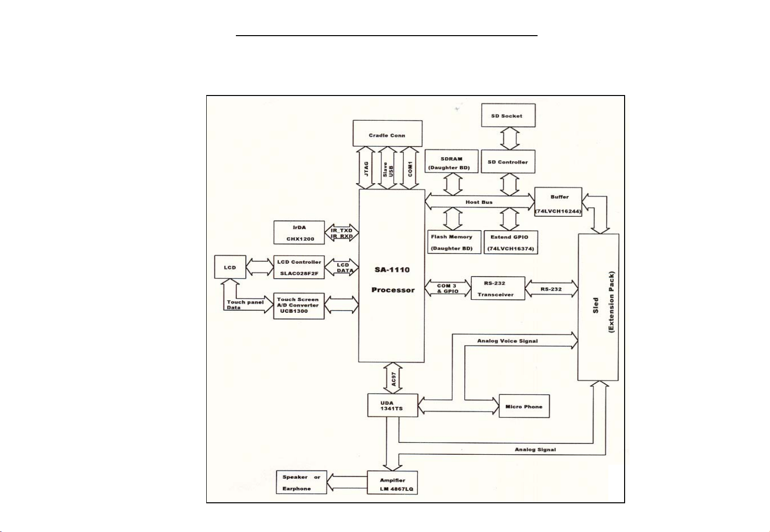
1.2.1 System Block Diagram
3
Page 5
Block Diagram
Barracuda PDA Maintenance
4
Page 6
Barracuda PDA Maintenance
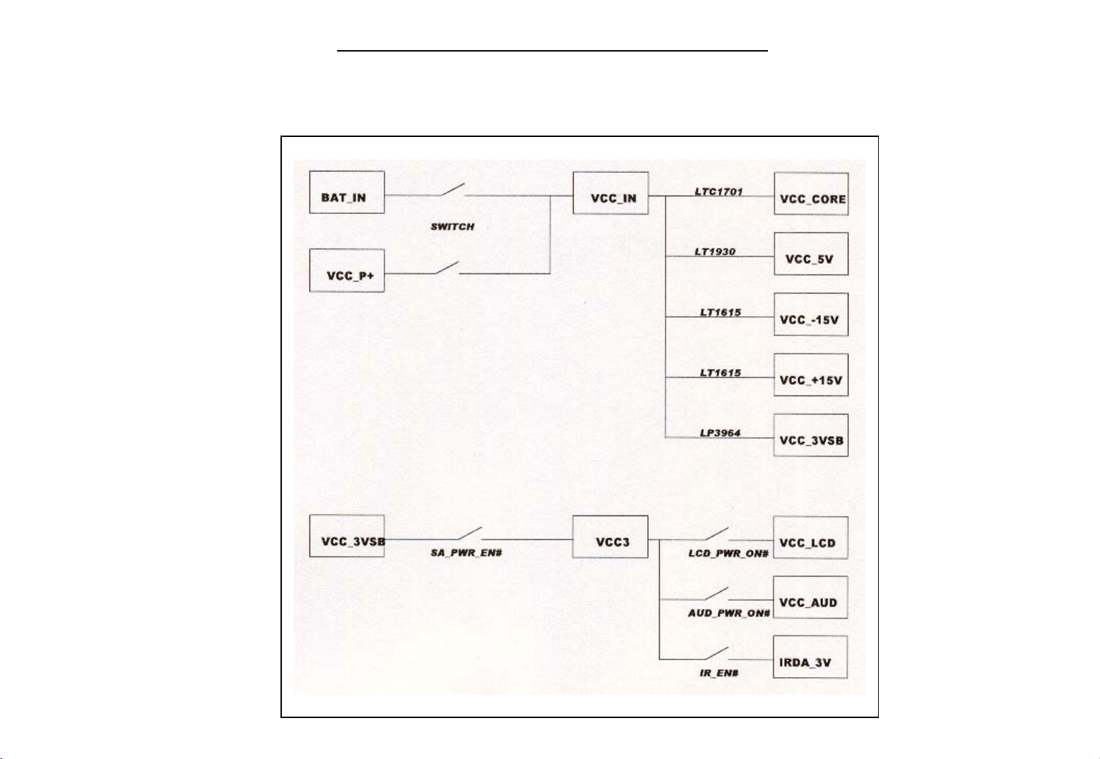
Power Block Diagram
5
Page 7

Barracuda PDA Maintenance
y
1.2.2 Main Board
1.2.2.1 CPU: Intel StrongARM SA1110-206MHz
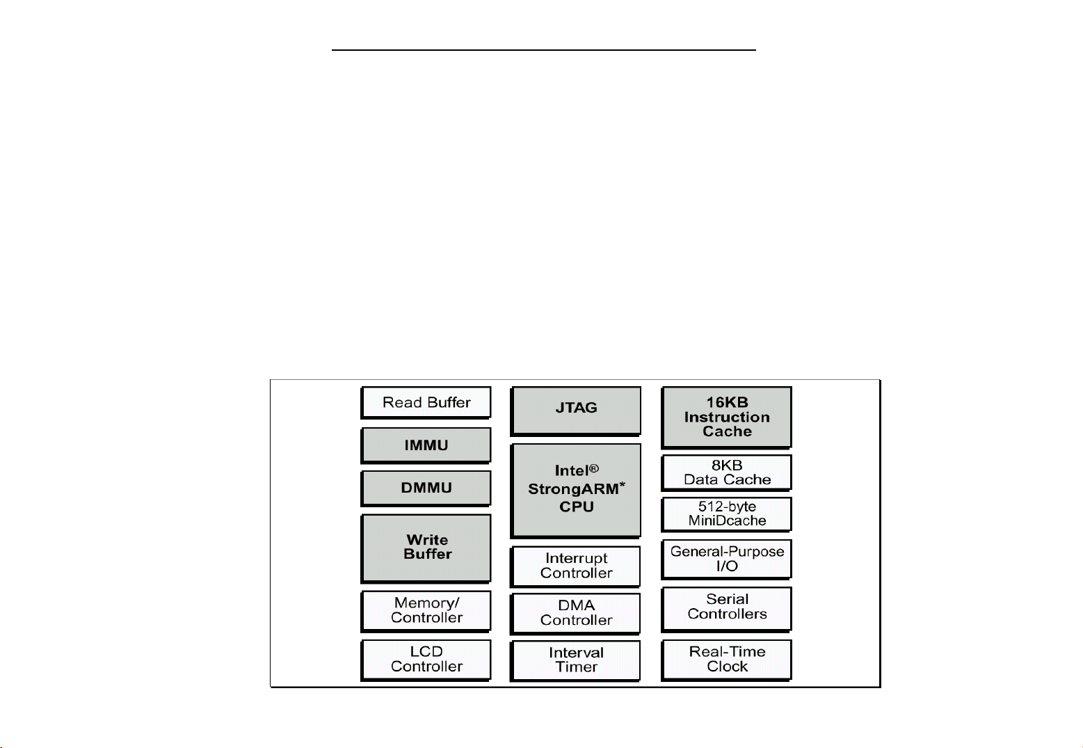
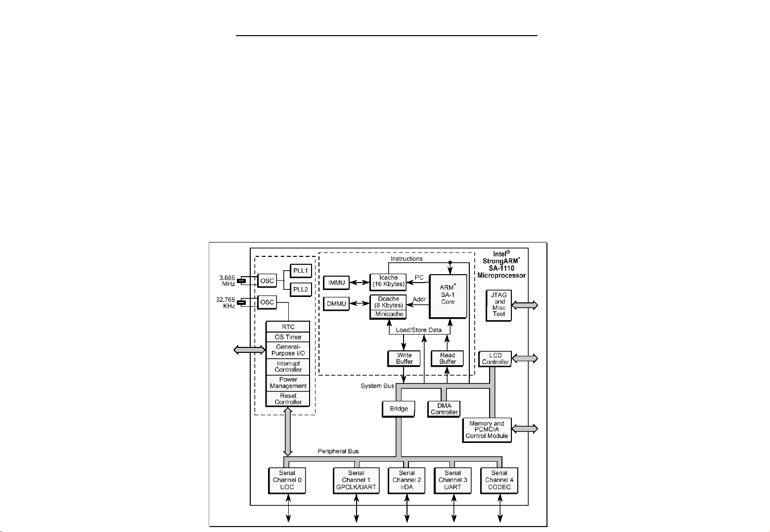
The SA-1110 is a general-purpose, 32-bit RISC microprocessor with a 16 Kbyte instruction cache, an 8 Kbyte
write-back data cache, a minicache, a write buffer, a read buffer, and a memory management unit (MMU)
combined in a single chip. The SA-1110 is software compatible with the ARM * V4 architecture processor famil
and can be used with ARM * support chips such as I/O, memory, and video.
Features of the SA-1110 CPU
High Performance -- 235 Dhrystone 2.1 MIPS @ 206 MHz
Low power (normal mode) -- <400 mW @ 1.75 V/206 MHz
Integrated clock generation
Internal phase-locked loop (PLL)
3.686 MHz oscillator
32.768 KHz oscillator
Power-management features
Normal (full-on) mode
Idle (power-down) mode
Sleep (power-down) mode
Big and little endian operating modes
3.3 V I/O interface
256-pin mini-BGA package (mBGA)
32-way set-associative caches
16 Kbyte instruction cache
8 Kbyte write-back data cach
32-entry memory-management units
Maps 4 Kbyte, 8 Kbyte, or 1 Mbyte
6
Page 8
Write buffer
8-entry, between 1 and 16 bytes each
Read buffer
4-entry, 1, 4, or 8 words
Memory bus
Interfaces to ROM, synchronous mask ROM (SMROM), Flash, SRAM, SRAM-like variable latency
I/O, DRAM, and synchronous DRAM (SDRAM)
Supports two PCMCIA sockets
SA-1110 Features
Barracuda PDA Maintenance
7
Page 9

Barracuda PDA Maintenance
r
p
The SA-1110 consists of the following functional blocks:
• Processing Core
The processor is the ARM * SA-1 core with a 16 Kbyte instruction cache (Icache) and 8 Kbyte data cache
(Dcache). The instruction (I) and data (D) streams are translated through independent
memory-management units (MMUs). Stores are made using a four-line write buffer. The performance of
specialized load routines is enhanced with the four-entry read buffer that can be used to prefetch data for
use at a later time. A 16-entry minicache provides a smaller and logically separate data cache that can be
used to enhance caching performance when dealing with large data structures.
• Memory and PCMCIA Control Module
The memory and PCMCIA control module (MPCM) supports four banks of fast-page-mode (FPM),
extended-data-out (EDO), and/or synchronous DRAM (SDRAM). It also supports up to six banks of static
memory: all six banks allow ROM or Flash memory, each with non-burst or burst read timings.
Additionally, the lower three static banks support SRAM, the upper three static banks support variable
latency I/O devices (with the variable data latency controlled by a shared data ready input), and the lower
four static banks support synchronous mask ROM (SMROM). SMROM is supported only on 32-bit data
busses. All other dynamic and static memory types and variable latency I/O devices are supported on eithe
16-bit or 32-bit data busses. Expansion devices are supported through PCMCIA control signals that share
the memory bus data and address lines to complete the card interface. Some external glue logic (buffers and
transceivers) is necessary to implement the interface. Control is provided to permit two card slots with
hot-swap capability.
•
Peripheral Control Module
The peripheral control module (PCM) contains a number of serial control devices, an LCD controller as
well as a six-channel DMA controller to provide service to these devices:
An LCD controller with support for passive or active displays
A universal serial bus (USB) endpoint controller
A serial controller with supporting 115 Kbps and 4 Mbps IrDA protocols
A 16550-like UART supporting 230 Kbps
A CODEC interface supporting Motorola SPI,National Microwire, TI Synchronous Serial, or the
Philli
s UCB1100 and UCB1200 protocol
8
Page 10
Barracuda PDA Maintenance
• System Control Module
The system control module (SCM) is also connected to the peripheral bus. It contains five blocks used for
general system functions:
A real-time clock (RTC) clocked from an independent 32.768 kHz oscillator
An operating system timer (OST) for general system timer functions as well as a watchdog mode
Twenty-eight general-purpose I/Os (GPIO)
An interrupt controller
A power-management controller that handles the transitions in and out of sleep and idle modes
A reset controller that handles the various reset sources on the processor
SA-1110 Block Diagram
9
Page 11

Barracuda PDA Maintenance
SA-1110 Processor LCD controller:
The SA-1110’s
Passive Color Mode
Active Color Mode
Passive Monochrome Mode
Display size up to 1024 x 1024 pixels are supported. However, the size of encoded pixel data within the frame
buffer limits the maximum size screen the LCD can drive due to memory bus bandwidth.
The LCD controller also supports single- or dual displays. Encoded pixel data is stored in external memorv in a
frame buffer in 4-, 8-, 12-, or 16-bit increments and is loaded into a 5-entry FIFO (32 bits per entry ) on a demand
basis using the LCD’s own dedicated dual-channel DMA controller. One channel is used for single-panel displays
and two are used for dual-panel displays.
Frame buffer data contains encoded pixel values that are used by the LCD controller as pointers to index into a
256-entry x 12-bit wide palette. Monochrome palette entries are 4 bits wide; color palette entries are 12 bits wide.
Encoded pixel data from the frame buffer. which is 4 bits wide, address the top 16 locations of the palette; 8-bit
pixel data accesses any the 256 entries within the palette. When passive color 12-bit pixel mode is enable, the
color pixel values bypass the palette and are fed directly to the LCD’s dither logic. When active color 16-bit pixel
mode is enabled, the pixel value not only bypasses the palette, but also bypasses the dither logic and is sent
directly to the LCD’s data pins.
LCD controller has three types of displays:
….. Supports a total of 375 possible colors, displaying any of 256 colors for each frame.
……Supports up to 65535 colors (16-bit).
… Supports 15 gray-scale levels.
Once the 4- or 8-bit encoded pixel value to select a palette entry, the value programmed within the entry is
transferred to the dither logic, which uses a patented space- and time- based dithering algorithm to produce
the pixel data that is output to the screen. Dithering causes individual pixels to be turned off on each frame at
varying rates to produce the 15 levels of gray for monochrome screen and 15 levels each for the red, green,
and blue pixel components for color screens, providing a total of 3375 colors (256 colors are available on each
frame). The data output from the dither logic is placed in a 19-entry pin data FIFO before it is placed out on the
LCD’s pins and driven to the display using pixel clock.
10
Page 12

Barracuda PDA Maintenance
Depending on the type of panel used, the LCD controller is programmed to use either 4-, 8-, or 16-pixel data
output pins. Single –panel monochrome displays use either four or eight data pins to output 4 or 8 pixels for each
pixel clock; single-panel color displays use eight pins to output 2-2/3 pixels each pixel clock ( 8 pins / 3 colors /
pixel = 2-2/3 pixels per clock ). The LCD controller also supports dual-panel mode, which causes the LCD
controller’s data lines to be split into two groups, one to drive the top half and one to drive the bottom half of the
screen. For dual-panel displays, the number of pixel data output pins is doubled, allowing twice as many pixels
to be output each pixel clock to the two halves of the screen.
In active color display mode, the LCD controller can drive TFT displays. The LCD’s line clock pin functions as a
horizontal sync ( HSYNC ) signal, the frame clock pin functions as a vertical sync ( VSYNC ) signal, and the ac
bias pin functions as an output enable ( OE ) signal. In TFT mode, the LCD’s dither logic is bypassed, sending
sending selected palette entries ( 12 bits each ) directly to the LCD’s data output pins. Additionally, 16-bit pixels
can be used that bypass both the palette and the dither logic.
The LCD controller can be configured in active color display mode and used with an external DAC ( and
optionally an external palette ) to drive a video monitor. Note that only monitors that implement the RGB
data format can be used; the LCD controller does not support the NTSC standard .
When the LCD controller is disabled, control of its pins is given to the peripheral pin controller ( PPC ) to
be used as general-purpose digital input/output pins that are noninterruptible. The LCD controller’s pins
include:
LDD 7:0
Data lines used to transmit either four or eight data values at a time to the LCD display. For
monochrome displays, each pin value represents a pixel; for passive color, groupings of three
pin values represent one pixel ( red, green, and blue data values ). In single-panel monochrome
mode, LDD 3:0 pins are used. For double-pixel data, single-panel monochrome, dual-panel
monochrome, single-panel color, and active color modes LDD 7:0 are used.
11
Page 13

GPIO 9:2
L_PCLK
L_LCLK
L_FCLK
Barracuda PDA Maintenance
when dual-panel color or 16 bit TFT operation is programmed, GPIO pins are used as the additional,
required LCD data lines to output pixel data to the screen.
Pixel clock used by the LCD display to clock the pixel data into the line shift register. In passive mode.
pixel clock transitions only when valid data is available on the data pins. In active mode, pixel clock
transitions continuously and the ac bias pin is used as an output to signal when data is available on
the LCD’s data pins.
Line clock used by the LCD display to signal the end of a line of pixels that transfers the line data from
the shift register to the screen and increment the line pointers. Also, it is used by TFT displays as the
horizontal synchronization signal.
Frame clock used by the LCD displays to signal the start of a new frame of pixels that resets the line
pointers to the top of the screen. Also, it is used by TFT displays as the vertical synchronization sibnal.
L_BIAS
AC bias used to signal the LCD display to switch the polarity of the power supplies to the row and
column axis of the screen to counteract DC offset. In TFT mode, it is used as as the output enable
to signal when data should be latched from the data pins using the pixel clock.
The pixel clock frequency is derived from the output of the on-chip PLL that is used to clock the CPU ( CCLK )
and is programmable from CCLK/6 to CCLK/514. each time new data is supplied to the LCD data pins, the
pixel clock is toggled to latch the data into the LCD display’s serial shifter.
12
Page 14

Barracuda PDA Maintenance
The line clock toggles after all pixels in a line have been transmitted to the LCD driver and a programmable
number of pixel clock wait states have elapsed both at the beginning and end of each line. In passive mode,
the frame clock is asserted during the first line of the screen. In active mode, the frame clock is asserted
at the beginning of each frame after a programmable number of line clock wait states occur. In passive
display mode, the pixel clock does nit transition when the line clock is asserted. However, in active display
mode, the pixel clock transitions continuously and the ac bias bin used as an output enable to signal when
valid pixels are present on the LCD’s data lines. In passive mode, the ac bias pin can be configured to
transition each time a programmable number of line clocks have elapsed to signal the display to reverse the
polarity of its voltage to counteract DC offset in the screen.
LCD Controller Operation
The LCD controller supports a variety of user-programmable options including display type and size frame
buffer, encoded pixel size, and output data width. Although all programmable combinations are possible,
the selection of displays available within the market dictate which combinations of these programmable
options are practical. The type of external memory system implemented by the user limits the bandwidth
of the LCD’s DMA controller, which, in turn, limits the size and type of screen that can be controlled. The
user must also determine the maximum bandwidth of the SA-1110’s external bus that the LCD is allowed
to use without negatively affecting all other functions that the SA-1110 must perform. Note that the LCD’s
DMA engine has highest priority on the SA-1110’s internal data bus structure ( ARM system bus ) and
can “starve” other masters on the bus, including the CPU.
The following sections describe individual functional blocks within the LCD controller, frame buffer and
palette memory organization, and the LCD’s DMA controller. The sections are arranged in order of data
flow, starting with the off-chip frame buffer and ending with the pins that interface to the LCD display.
13
Page 15

Barracuda PDA Maintenance
t
d
1.2.2.2 UDA1341TS Economy audio CODEC
The UDT1341TS is a single-chip stereo Analog-to-Digital Converter (ADC) and Digital-to-Analog Converter
(DAC) with signal processing features employing bit stream conversion techniques. It's fully integrated analog.
Front end, including Programmable Gain Amplifier (PGA) and a digital Automatic Gain Control (AGC). Digital
Sound Processing (DSP) featuring makes the device an excellent choice for primary home stereo MiNi Disc
applications, but by virtue of its low power and low voltage characteristics it is also suitable for Portable applications
such as MD/CD boom boxes, notebooks PCs and digital video cameras.
The UDA1341TS is similar to the UDA1340M and the UDA1344TS but adds features such as digital mixing of
Two input signals and one channel with a PGA and a digital AGC. The UDA1341TS supports the I
2
S-bus data forma
with word lengths of up to 20 bits, the MSB-justified data format.
With word lengths of up to 20 bits, the LSB-justified serial data format with word lengths of 16,18 and 20 bits an
three combinations of MSB data output combined with LSB 16,18 and 20 bits data input.
The UDA1341TS has DSP features in playback mode like de-emphasis, volume, bass boots, treble and soft mute.
Which can be controlled via the L3-interface with a micro-controller.
Features:
General
Low power consumption
3.0V power supply
256f
, 384fs or 512fs system clock frequencies ( f
s
Small package size ( SSOP28 )
Partially pin compatible with UDA1340M and UDA1344TS
Fully integrated analog front end including digital AGC
ADC plus integrated high-pass filter to cancel DC offset
ADC supports 2V ( RMS value ) input signals
Overload detector for easy record level control
Separate power control for ADC and DAC
Easy application
Functions controllable via L3-interface
sys
)
14
Page 16

Barracuda PDA Maintenance
Multiple format data interface
2
S-bus, MSB-justified and LSB-justified format compatible
I
Three combinational data formats with MSB data output and LSB 16, 18 or 20 bits data input
1fs input and output format data rate
DAC digital sound processing
Digital dB-linear volume control ( low microcontroller load )
Digital tone control, bass boots and treble
Digital de-emphasis for 32, 44.1 or 48 kHz audio sample frequencies ( f
Soft mute
Advanced audio configuration
DAC and ADC polarity control
Two channel stereo single-ended input configuration
Microphone input with on-board PGA
Optional differential input configuration for enhanced ADC sound quality
Stereo line output ( under microcontroller volume control )
Digital peak level detection
High linearity, dynamic range and low distortion
)
s
15
Page 17

Barracuda PDA Maintenance
p
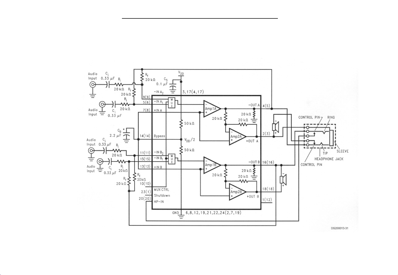
1.2.2.3 Audio Amplifier: NS LM4867
General Description
The LM4867 is a dual bridge-connected audio power amplifier which, when connected to a 5V supply, will
deliver 2.1W to a 4Ω load or 2.4W to a 3Ω load with less than 1.0% THD+N. The LM4867 uses advanced, latest
generation circuitry to eliminate all traces of clicks and pops when the supply voltage is first applied. The
amplifier has a headphone-amplifier-select input pin. It is used to switch the amplifiers from bridge to
single-ended mode for driving headphones. A new circuit topology eliminates headphone output coupling
capacitors. A MUX control pin allows selection between the two sets of stereo input signals. The MUX
control can also be used to select between two different customer-specified closed-loop responses.
Boomer audio power amplifiers are designed specifically to
mount package and require few external components. To simplify audio system design, the LM4867 combines
dual bridge speaker amplifiers and stereo headphone amplifiers in one package.
The LM4867 features an externally controlled power-saving micropower shutdown mode, a stereo
headphone amplifier mode, and thermal shutdown protection.
Features
Advanced “click and pop” suppression circuitry
Eliminates headphone amplifier output coupling capacitors
Stereo headphone amplifier mode
Input mux control and two separate inputs per channel
Thermal shutdown protection circuitry
LLP, TSSOP, and exposed-DAP TSSOP packaging available
rovide high quality output power from a surface
16
Page 18
Barracuda PDA Maintenance
Typical Audio Amplifier Application Circuit
17
Page 19

Barracuda PDA Maintenance
d
p
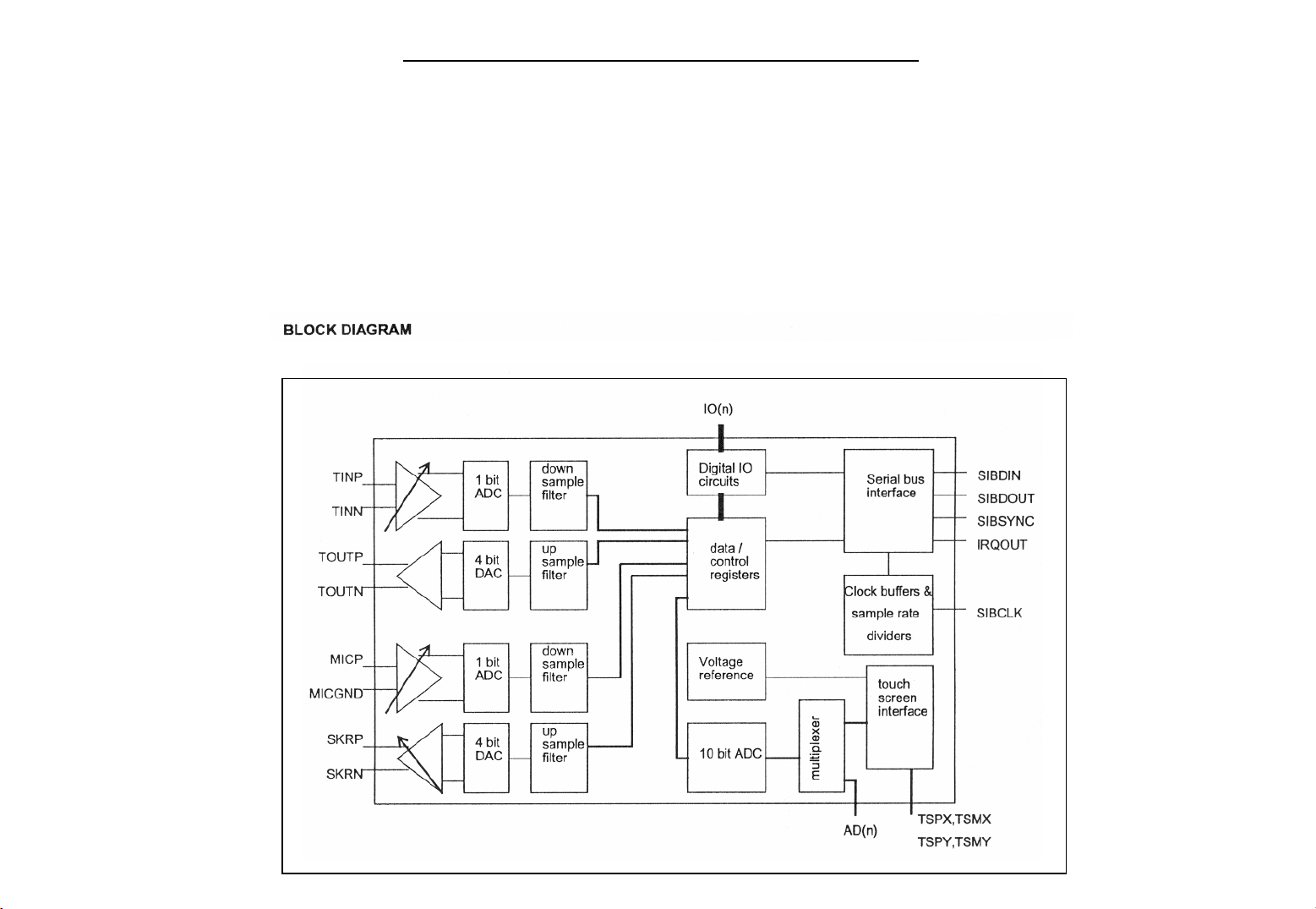
1.2.2.4 Touch Screen Controller Chip with ADC: Philips semiconductors UCB1300
General Description
The UCB1300 is a single chip, integrated mixed signal audio and telecom codec. The single channel audio codec
is designed for direct connection of a microphone and a speaker. The built-in telecom codec can directly be connecte
to a DAA and supports high speed modem protocols. The incorporated analog-to-digital converter and the touch
screen interface provides complete control and read-out of an 4 wire resistive touch screen. The 10 general purpose
I/O pins provide programmable inputs and/or outputs to the system.
The UCB1300 has a serial interface bus (SIB) intended to communicate to the system controller. Both the codec
input data and codec output data and the control register data are multiplexed on this SIB interface.
Features
48 pin LQFP (SOT313-2) small body SMD package and low external component count results in minimal PCB
space
12-bit sigma delta audio codec with programmable sample rate, input and output voltage levels, capable of
connecting directly to speaker and microphone, including digitally controlled mute, loopback and clip
detection functions
14-bit sigma delta telecom codec with programmable sample rate, including digitally controlled in
level, mute, loopback and clip detection functions. The telecom codec can be directly connected to a Data
Access Arrangement (DAA) and includes a built in sidetone suppression circuit.
Complete 4 wire resistive touch screen interface circuit supporting position, pressure and plate resistance
Measurements
10-bit successive approximation ADC with internal track and hold circuit and analog multiplexer for touch
screen read-out and monitoring of four external high voltage (7.5V) analog voltages
High speed, 4 wire serial interface data bus (SIB) for communication to the system controller
ut voltage
18
Page 20
3.3V supply voltage and built in power saving modes make the UCB1300 optimal for portable and battery
powered applications
Maximum operating current 25 mA
10 general purpose IO pins
UCB1300 Block Diagram
Barracuda PDA Maintenance
19
Page 21

Barracuda PDA Maintenance
f
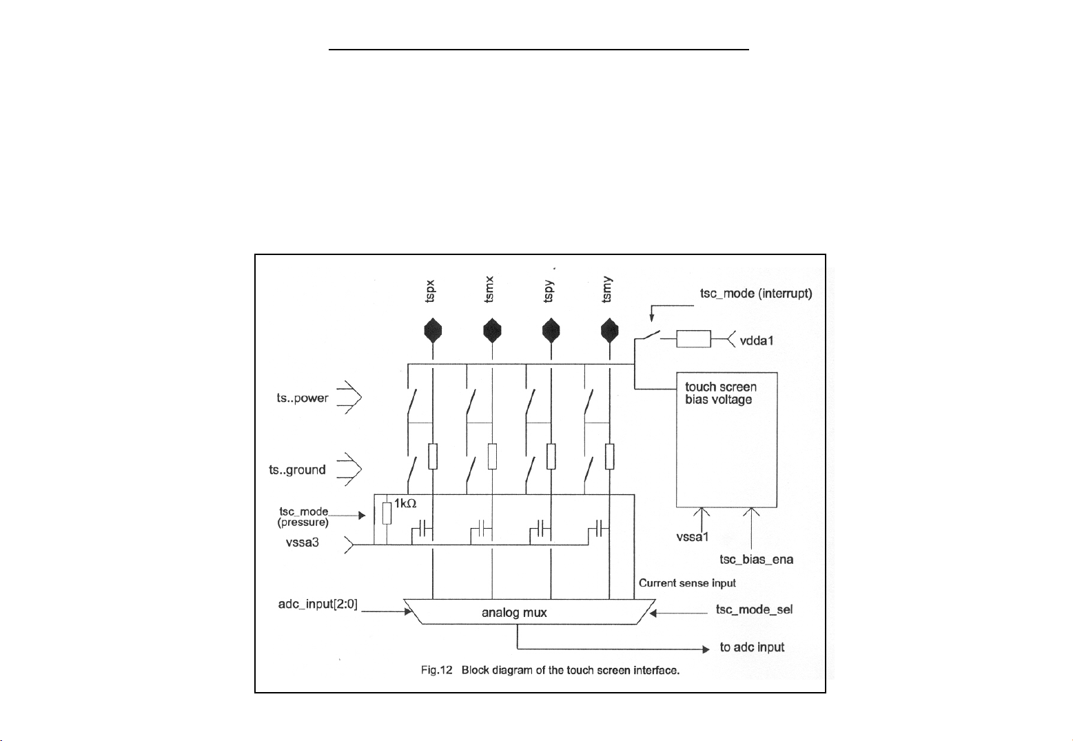
TOUCH SCREEN INTERFACE
performing position, pressure and plate resistance measurements. In addition, the touch screen can be programmed to
generate interrupts when the touch screen is pressed. The last mode is also active when the UCB1300 is set in the
stand-by mode.
these pins can be programmed to be floating, powered or grounded in the touch screen switch matrix. The setting of
each touch screen pin is programmable through the touch screen control register. Possible conflicting settings
(grounding and powering of a touch screen pin at the same time) are detected by the UCB1300. In that case, the touch
screen pin will be grounded.
the plates configuration, the touch screen interface should be programmed to pressure mode for the duration 1 SIB
frame before resuming a position measurement.
This makes the touch screen biasing independent of supply voltage and temperature variations. Four low pass filters,
one on each touch screen terminal, are built in to minimize the noise coupled from the LCD into the touch screen
signals. An LCD typically generates large noise glitches on the touch screen, since they are closely coupled .The
influence of the glitches can nevertheless be minimized by performing measurements when the LCD is quiet. This
can be done by synchronizing the measurement and the video driver with the ADCSYNC pin.
The UCB1300 contains a universal resistive touch screen interface for 4-wire resistive touch screen, capable of
The touch screen interface connects to the touch screen by four wires: TSPX, TSMX, TSPY and TSMY. Each o
In position mode, opening the TS..gnd switch can take a long time. To avoid unpredictable delays after changing
The UCB1300's internal voltage reference (Vref ) is used as reference voltage for the touch screen bias circuit.
In addition to the measurements mentioned above, the touch screen can also act as an interrupt source. In this
mode the X plate of the touch screen has to be powered and the Y plate has to be grounded. In this case the touch
screen is not biased by the active touch screen bias circuit, but by a resistor to VDDA1 . This configuration simply
biases the touch screen and the UCB1300 does not consume power unless the touch screen is touched. The voltage on
the X plate terminals drops if the screen is pressed. This voltage drop is detected by Schmitt-trigger circuits, of which
the outputs are connected to the interrupt control block. A touch screen interrupt is generated either when the touch
screen is pressed (falling edge enabled) or when the touch screen is released (rising edge enabled). It can be used to
activate the system around the UCB1300 to start a touch screen read-out sequence. The internal Schmitt-trigger
circuits are connected to the TSPX and TSMX signals after the built-in low pass filters. This reduces the number of
spurious interrupts, due to the coupling between the LCD screen and the touch screen sensors.
20
Page 22
Barracuda PDA Maintenance
Each of the four touch screen signals can be selected as input for the built-in 10-bit ADC, which is used to
determine the voltage on the selected touch screen pin. The flexible switch matrix and the multi-functional touch
screen bias circuit enables the user of the UCB1300 to set each desired touch screen configuration.
Block diagram of the touch screen interface
21
Page 23

Barracuda PDA Maintenance
t
10-BIT ADC
The UCB1300 includes a 10-bit successive approximation analog-to-digital converter (ADC) with built-in track
and hold circuit and an analog multiplexer to select one of the 4 analog inputs (AD0 - AD3), the 4 touch screen inputs
(TSPX, TSMX, TSPY, TSMY) or the pressure output of the touch screen bias circuit. The ADC is used to read-out the
touch screen inputs and it measures the voltage on the four analog high voltage inputs AD0 - AD3. The analog
multiplexer contains 4 resistive dividers to attenuate the high voltage on the AD0 - AD3 inputs to the ADC input
range.
The ADC is controlled completely through the SIB interface, but the UCB1300 contains internal logic to ease the
control of the ADC and to minimize the number of SIB frame read/write actions.
A complete ADC control sequence analog to digital conversion consists of several phases. Firstly, the ADC has to
be enabled; secondly, the input selector must be set to the proper input; thirdly, the ADC conversion has to be started;
and finally, the ADC result has to be read from register 11.
The ADC is activated by setting ADC_ENA in register 10. The ADC circuit, including the track and hold circui
does not consume any power as long as this bit is reset. The analog input multiplexer is controlled by ADC_INPUT[n]
and the ADC is actually started with the ADC_START bit. When TSPX and TSMX are in the interrupt mode, the ADC
cannot be started, even to measure AD0-3.
The UCB1300 has two different modes to start the ADC conversion, which are selected by the
ADC_SYNC_ENA bit. The default mode is the non-synchronization mode, in which the conversion is started directly
with a 0-to-1 transition of ADC_START. Secondly the ADC is started at a rising edge of the signal applied to the
ADCSYNC pin if ADC_SYNC_ENA is set. Activating the ADC while keeping the start logic in the started state
(ADC_START = 1) will lead to unpredictable behavior and the value of the ADC data register will not be meaningful.
Always activate a start sequence for each acquisition (0-to-1 transition on the internal ADC_START signal).
22
Page 24

Barracuda PDA Maintenance
Block diagram of the 10-bit ADC circuit
23
Page 25

Barracuda PDA Maintenance
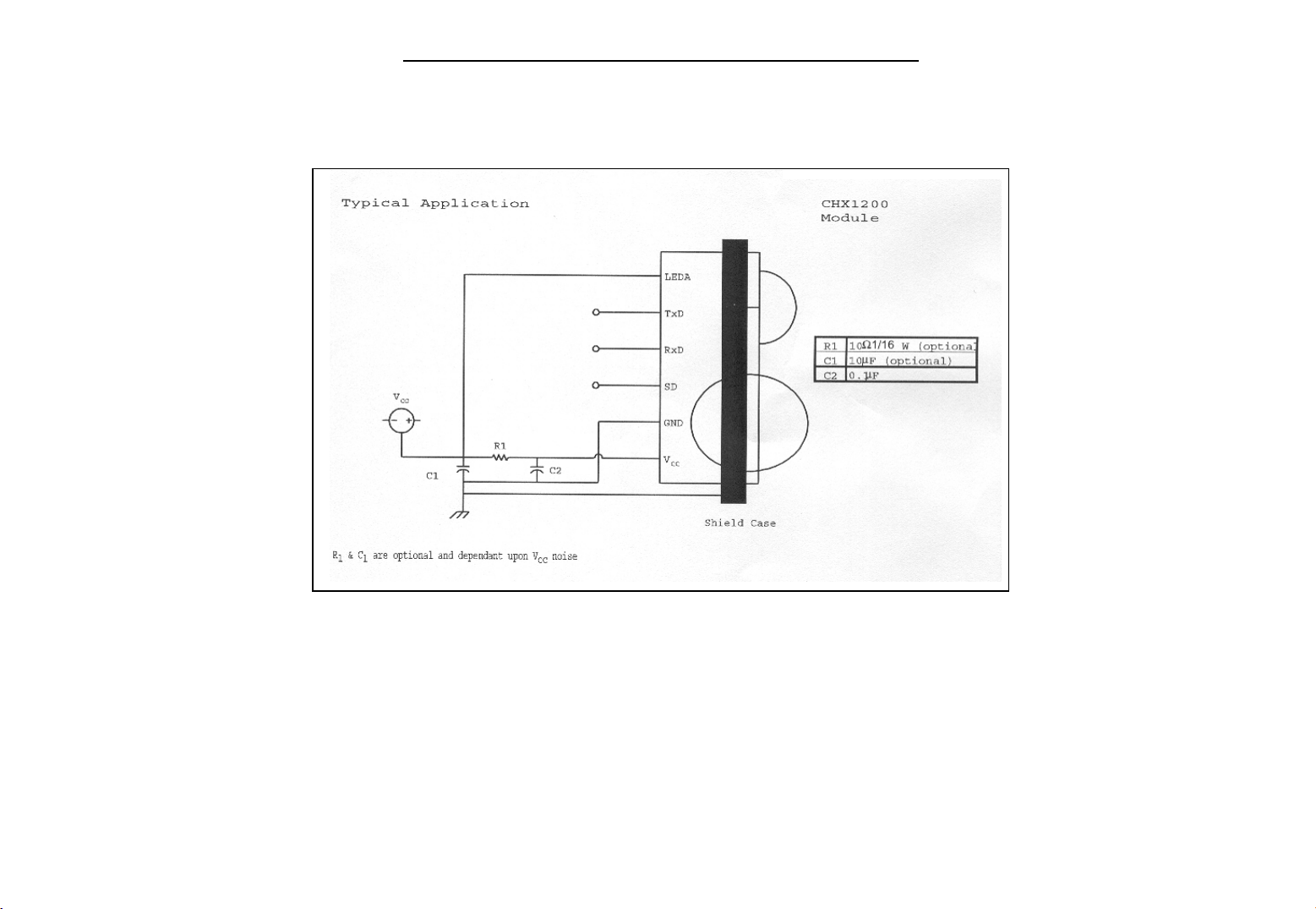
.2.2.5 Infrared Component: CHX 1200
The CHX1200 is an Low Power SIR (IrMC) Transceiver. The CALIBRE CHX1200 is an ideal transceiver
for mobile communication applications in today’s ultra-compact power conscious portable products, such as
mobile phones, pagers or PDA’s. Specifically designed to support IrDA-IrMC Low power SIR mode, the
transceiver combines an IRED emitter, a PIN photodiode detector, a digital AC coupled LED driver and a fully
differential receiver/decoder in a single, miniature package. The CALIBRE CHX1200 provides an efficient
implementation of the low power SIR standard in a small footprint format. Application circuit space is also
minimized, as only one capacitor is required to complete the solution.
Features
Compliant to IrDA SIR Specification 1.2 Low Power SIR
Low supply voltage range, 2.7 to 3.6V
0.2mA (max) Shutdown
Low Power ,95uA (typ.) @ 3.3V
Ultra small form factor (6.8mm L x 2.8mm W x 2.2mm H)
External components : one capacitor
Extended Operating Temp. Range (-30 to + 85 oC)
Pin Compaitble with HP HSDL-3201 and Sharp GP2W0104YP
I LED =35mA @ 3.6 mW/sr
(Minimum Link Distance 20cm)
24
Page 26
BLOCK DIAGRAM
Barracuda PDA Maintenance
25
Page 27

Barracuda PDA Maintenance
b
b
1.2.2.6 W86L388D SD Controller
General Description
The W86L388D is a SD/MMC host interface bridge used between host microprocessor and SD/MMC .
The data width of host microprocessor can be 8-
of host interface. It also supports DMA or interrupt type of transfer mode to improve data transfer performance
etween host microprocessor and SD/MMC. W86L388D is fit for most of IA devices, such as PDA, Cellular Phone,
DSC, and MP# player.
Features
Compliant with SD spec. Version 1.0
Compliant with MMC spec. Version 2.2
Support two types of host microprocessor interface access-synchronous and
asynchronous mode
DMA and interrupt transfer mode supported
Host microprocessor 8/16 bit data bus
Built-in crystal driver circuit, support external oscillator or crystal clock
Extra 5 programmable GPIO supported
Wide range of clock input from 3.58MHz up to 25MHz
3.3V operation
48-pin LQFP package
it W86L388D can support synchronous or asynchronous type
26
Page 28
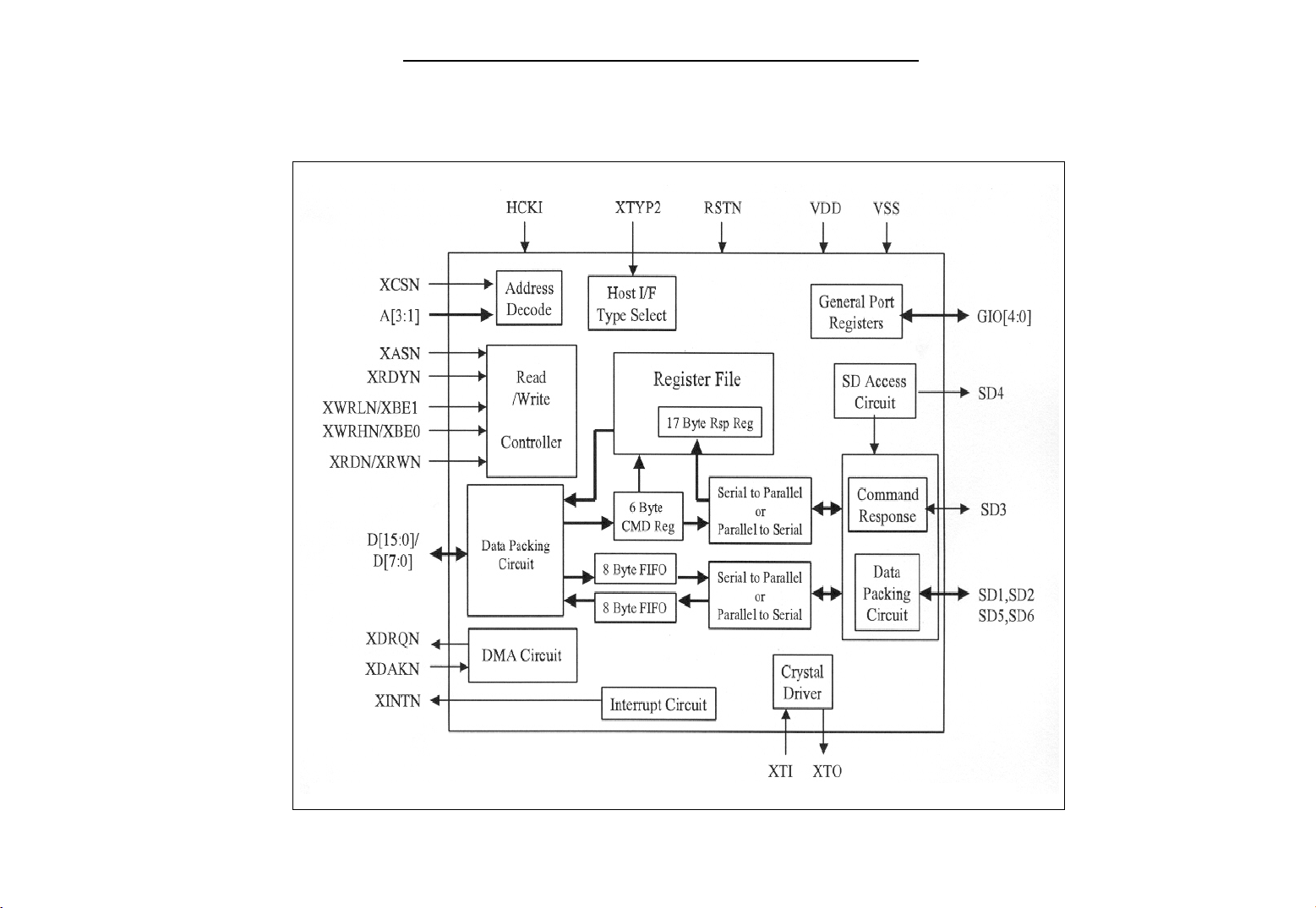
Block Diagram
Barracuda PDA Maintenance
27
Page 29

Barracuda PDA Maintenance
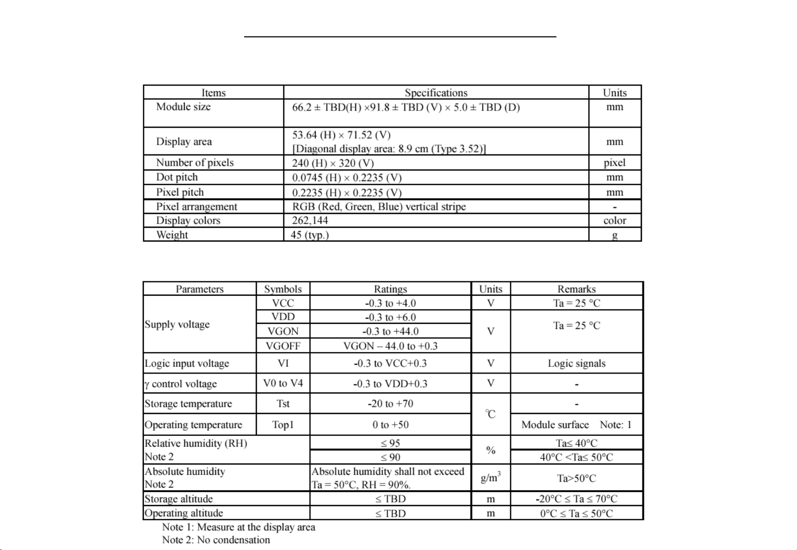
1.2.2.7 Display LCD Module: NEC QVGA Reflective Color LCD Module
MODEL NAME: NL2432DR22-03B
Features
Number of pixels: 240 (H) x 320 (V)
Drive system: a-Si TFT active matrix
Pixel pitch: 0.2235(H) x 0.2235 (V) mm
Number of colors: 262,144
Weight: 45 g(Typ.)
Contrast time: 10:1(Typ. : With Front light and Touch panel)
Reference: 40:1(Without Front light and Touch panel)
Response time: 32ms (Typ., Ton + Toff)
Reflection ratio: 17%(Typ. With Front light and Touch panel)
Reference: 35% (Without Front light and Touch panel)
Supply voltage: VCC 3.0V (typ. Logic)
VDD 5.0V (typ. ? control)
VGON 15.0 (LCD driving)
VGOFF –15.0V (LCD driving)
Low power consumption: 25mW ( typ. )
28
Page 30
Barracuda PDA Maintenance
GENERAL SPECIFICATIONS
ABSOLUTE MAXIMUM RATINGS
29
Page 31

Barracuda PDA Maintenance
1.2.2.7-1 Touch Panel: Gunze Touch panel 3.5”
General Specifications
Name of product : Film-Glass Touch Panel
Rating : DC5.5V max,
Insulation resistance :10M or more at DC25V
Static electricity : 15kV 150 150 pF
Capacitance : Less than 200 nF
Chattering : Less than 20 ms
Operational starting force : 0.1 0.8N
Linearity : Less than 15%
Input method : Finger or R = 0.8 mm polyacetal stylus
Transparency : 78 ~ 84%
Reflective : about 20%
Surface hardness : 3H or more
Point hitting life : R=3mm Sillicone rubber : 1,000,000 times input
2.94N pressure , 3 times/sec
Character writing life : R=0.8mm polyacetal stylus : 100,000 Chara. input
2.45N pressure , 5000words/hour
1.2.2.8 LED Display
Charger: Battery Charger Indicator ( Amber )
The Amber will be enable while charging .
Notification
When system occur alarm or schedule on time the LED will flash
30
Page 32

Barracuda PDA Maintenance
r
f
1.2.2.9 RS-232 Transceivers: SP3243E
DESCRIPTION
The SP3223E and 3243E products are RS-232 transceiver solutions intended for portable or hand-held
applications such as notebook and palmtop computers. The SP3223E and 3243E Use an internal high-efficiency,
charge-pump power supply that requiresonly0.1mFcapacitors in 3.3V operation. This charge pump and Sipex's
driver architecture allow the SP3223E/ 3243E series to deliver compliant RS-232 performance from a single powe
supply ranging from +3.3V to +5.0V. The SP3223E is a 2-driver/2-receiver device, and the SP3243E is a
3-driver/5-receiver device ideal for laptop/notebook computer and PDA applications.
The SP3243E includes one complementary receiver that remains alert to monitor an external device's Ring
Indicate signal while the device is shutdown.
The Auto-Online feature allows the device to automatically "wake-up" during a shutdown state when an
RS-232 cable is connected and a connected peripheral is turned on. Otherwise, the device automatically shuts itsel
down drawing less than 1mA.
Features
Meets true EIA/TIA-232-F Standards from a +3.0V to +5.5V power supply
Interoperable with EIA/TIA-232 and adheres to EIA/TIA-562 down to a +2.7V power source
Auto-Online ?circuitry automatically wakes up from a 1mA shutdown
Minimum 120Kbps data rate under load
Regulated Charge Pump Yields Stable RS-232 Outputs Regardless of VCC Variations
Enhanced ESD Specifications:
+15KV Human Body Model
+15KV IEC1000-4-2 Air Discharge
+8KV IEC1000-4-2 Contact Discharge
31
Page 33

Barracuda PDA Maintenance
32
Page 34

Barracuda PDA Maintenance
1.2.2.10 I²C Bus Serial EEPROM
DESCRIPTION
The Microchip Technology Inc. 24AA00/24LC00/24C00 (24xx00*) is a 128-bit Electrically Erasable PROM
memory organized as 16 x 8 with a 2-wire serial inter-face. Low voltage design permits operation down to 1.8 volts
for the 24xx00 version, and every version maintains a maximum standby current of only 1 mA and typical active
current of only 500 mA. This device was designed where a small amount of EEPROM is needed for the storage of
calibration values, ID numbers or manufacturing information, etc.The 24xx00 is available in 8ld PDIP, 8ld SOIC (150
mil), 8ld TSSOP and the 5ld SOT-23 packages.
Features
Low power CMOS technology
- 500 mA typical active current
- 500 nA typical standby current
Organized as 16 bytes x 8 bits
2-wire serial interface bus, I 2 C?compatible
100kHz (1.8V) and 400kHz (5V) compatibility
Self-timed write cycle (including auto-erase)
4 ms maximum byte write cycle time
1,000,000 erase/write cycles guaranteed
ESD protection > 4kV
Data retention > 200 years
8L DIP, SOIC, TSSOP and 5L SOT-23 packages
Temperature ranges available:
- Commercial (C): 0
- Industrial (I): -40℃ to +85℃
- Automotive (E) -40
to +70℃
℃
to +125℃
℃
33
Page 35

Barracuda PDA Maintenance
1.2.3 Internal I/O Device:
1.2.3.1 Internal Speaker * 1
Model NO. FG-15N081
Type: Mylar Cone Type
Nominal Size: 15mm inch
Voice Coil: 8? +/- 15% at 1500 Hz
Resonance FO: 780 Hz +/- 20% Hz
S.P.L: 75 Db +/- 3db at 0.5W Average at 800,1000,1200,1500 Hz
Power Rating: Normal 400 mW Maximum 500 mW
Distortion: 5% Maximum at 1000 Hz 400 mW
Total Weight: 1.7 g
Magnet: Materials: Ndfe-B Size: 6.6 X 1.5 mm
Flux Density: 4800 Gauss +/- 10 %
Low Temperature Test: Low temperature : -20℃ +/- 2℃
Highht temperature: +70
+/- 2℃
℃
1.2.3.2 Internal Microphone * 1
Electrical Characteristics Test Condition (Vs=2.0V RL=2.2Kohm Te=20° C R.H.=60%)
Sensitivity: -45 +/- 4dB(0dB=1V/Pa, 1kHz)
Impedance: 2.2Kohm
Directivity: Omnidirectional
Frequency: 20-16,000Hz
Max. Operation voltage: 10V
Standard operation voltage: 2V
Current consumption: 0.5mA
S/N ratio: 58dB
Sensitivity reduction: -3dB(0dB=1V/Pa, 1kHz Vs=1.5V)
34
Page 36

1.2.4 GPIO Table:
Barracuda PDA Maintenance
GPIO
Name
GPIO-0 BTN_PWR# I L ACT Power button to control system run/sleep
GPIO-1 KEY_PRESS# I L ACT Button / Switch press detection
GPIO-2 LCD_G3 O L LCD data output
GPIO-3 LCD_G4 O L LCD data output
GPIO-4 LCD_G5 O L LCD data output
GPIO-5 LCD_R1 O L LCD data output
GPIO-6 LCD_R2 O L LCD data output
GPIO-7 LCD_R3 O L LCD data output
GPIO-8 LCD_R4 O L LCD data output
GPIO-9 LCD_R5 O L LCD data output
GPIO-10 SSP_TXD O L SSP_UDA1341_TXD
GPIO-11 SSP_RXD I L SSP_UDA1341_RXD
GPIO-12 CLK_SSP O L SSP_UDA1341_SCLK
GPIO-13 SSP_SFRM O L SSP_UDA1341_SFRM
GPIO-14 AC_IN# I L ACT AC plug-in indication
GPIO-15 DCD#_WAKE I H ACT Serial port DCD signal , can wake up
GPIO-16 CRADLE_IN I H ACT Detect PDA plug into cradle
GPIO-17 GAUGE1 I/O H/L Gauge for main battery
GPIO-18 GAUGE2 I/O H/L Gauge for Sled battery
GPIO-19 CLK_UDA I H/L L Extend Audio clock 11.2896MHz
GPIO-20 BAT_FAULT_EN O H L Enable hardware battery fault if pass to
Function Name
I/O
Pin
H/L
active
Sleep
mode
state
Description
and backlight ON/OFF
system when in sleep mode
SA1110 BAT_FAULT
35
Page 37

Barracuda PDA Maintenance
GPIO
Name
GPIO-21 SLOT1_IRQ# I L L Sled card 1 interrupt
GPIO-22 SLOT2_IRQ# I L L Sled card 2 interrupt
GPIO-23 UCB_IRQ I H L UCB1300 interrupt output
GPIO-24 SA_CDKT1# I L H Sled card 1 insert detection
GPIO-25 SA_CDKT2# I L H Sled card 2 insert detection
GPIO-26 IRQ_SD# I L L SD interrupt
GPIO-27 BAT_FAULT_IRQ# I L L Hardware battery fault & cover out
External
GPIO
U10-1Q1 EXT_PWR_ON# O L L Sled / CF buffer power control pin
U10-1Q2 SA_RST1 O H L Card socket1 reset signal (In I/O and
U10-1Q3 UCB_RESET# O L L UCB 1300 reset signal
U10-1Q4 5V_PWR_ON O H L 5V power plane ON/OFF control (For
U10-1Q5 SA_RST2 O H L Card socket2 reset signal (In I/O and
U10-1Q6 LCD_ON O H L LCD output enable control pin ( High
U10-1Q7 LCD_PWR_ON# O L L LCD power plane ON/OFF control
U10-1Q8 EXT_BUS_ON# O L L Sled / CF buffer output enable
Function Name
I/O
Pin
H/L
active
Sleep
mode
state
Description
interruption to SA1110
memory mode => active high , IDE
mode => active low)
panel)
memory mode => active high , IDE
mode => active low)
=> output , L => disable)
(For NEC controller)
36
Page 38

Barracuda PDA Maintenance
GPIO
Name
U10-2Q1 AUD_PWR_ON# O L L Audio / Amplifier power plane
U10-2Q2 BL_ON/OFF# O H/L L Backlight ON(H)/OFF(L) control
U10-2Q3 IR_EN# O L L IR power ON/OFF control
U10-2Q4 QMUTE O H L Mute the audio codec UDA1341
U10-2Q5 LED_NOTE O H L Flash LED ( H=> flash , L => No
U10-2Q6 BL_ADJ_INC# O H/L L Backlight adjust data latch
U10-2Q7 BL_ADJ_U/D# O H/L L Backlight adjust data
U10-2Q8 CODEC_RESET# O L L Audio chip (UDA1341)reset
U12-1Q1 COM1_DTR# O L COM1 signal
U12-1Q2 COM1_RTS# O L COM1 signal
U12-1Q3 COM3_DTR# O L COM3 signal
U12-1Q4 COM3_RTS# O L COM3 signal
U12-1Q5 A0VPP O L PCMCIA power switch control
U12-1Q6 A1VPP O L PCMCIA power switch control
U12-1Q7 SLOT0_EN0 O L PCMCIA power switch control
U12-1Q8 SLOT0_EN1 O L PCMCIA power switch control
U12-2Q1 COM1_RI I L COM1 signal
U12-2Q2 COM1_CTS# I L COM1 signal
U12-2Q3 COM1_DCD# I L COM1 signal
U12-2Q4 COM1_DSR# I L COM1 signal
U12-2Q5 COM3_RI I L COM3 signal
U12-2Q6 COM3_CTS# I L COM3 signal
U12-2Q7 COM3_DCD# I L COM3 signal
U12-2Q8 COM3_DSR# I L COM3 signal
Function Name
I/O
Pin
H/L
active
Sleep
mode
state
Description
ON/OFF control
light )
37
Page 39

Barracuda PDA Maintenance
GPIO
Name
UCB1300
GPIO
IO_0 SA_CDEXT I H L Sled inserted detection
IO_1 L3_I2C_SDA I/O H/L L To Audio codec(UDA1341) L3
IO_2 L3_I2C_MODE O H/L L To Audio codec(UDA1341) L3
IO_3 L3_I2C_SCL O H/L L To Audio codec(UDA1341) L3
IO_4 EXT_PWROK I H L Sled Power_good signal (Only
IO_5 CHARGE_DET# I L L Main battery charge detection
IO_6 O L L
IO_7 I2C_SCL O H/L L I2C Clock signal
IO_8 I2C_SDA I/O H/L L I2C data signal
IO_9 ADC_SYNC L Can't be used as GPIO
ADC_0 BUTTON_DET RECORD , TASK , MEMO ,
ADC_1 TEMP Main battery temperature
ADC_2 L/S# Long / Short Sled detection ( H
ADC_3 VCC_BK Backup battery voltage sense
Function Name
I/O
Pin
H/L
active
Sleep
mode
state
Description
port , data signal
port , mode signal
port , clock signal
PCMCIA power is applying)
(Only activity in operating
mode )
CALENDAR , CONTACT ,
Jogdial
detection
=> Long , L => Short )
38
Page 40

Barracuda PDA Maintenance
1.2.5 Battery Fault
There are two kind of battery fault events which can force the system shutdown to prevent data lose .
1.2.5.1 Battery capacity low
While battery capacity below 3.4V , the hardware comparator will assert signal
CPU to save data to SDRAM and execute SDRAM self-refresh command , then assert
Hardware Battery Fault mechanism (SA1110 ) which force system shutdown .
BAT_FAULT_IRQ#
BAT_FAULT_EN
to interrupt
to enable
1.2.5.2 Battery cover lose
Since Capricorn battery is swappable , user has the way to access battery . The battery mechanical cover must be
monitored to ensure Capricorn battery is connected well without battery dropout problem . while battery cover be
removed , that will release one switch button and cause the signal
will be the same as battery capacity low event .
BAT_FAULT_IRQ#
be active , then the routine
39
Page 41

Barracuda PDA Maintenance
1.3 Memory system
1.3.1 Memory board
1.3.1.1 System Memory SDRAM
1.3.1.1-1 Winbond 128M-bit (8M X 16) Synchronous DRAM
Description:
40
Page 42

Barracuda PDA Maintenance
41
Page 43

Barracuda PDA Maintenance
42
Page 44

Barracuda PDA Maintenance
1.3.1.1-2 Samsung 128M-bit (8M X 16) Synchronous DRAM
Description:
The K4S281632C is 134,217,728 bits synchronous high data rate Dynamic RAM organized as 4 x 2,097,152 words
by 16bits, fabricated with SAMSUNG
precise cycle controls with the use of system clock I/O transactions are possible on every clock cycle. Range of
operating frequencies, programmable burst length and programmable latencies allow the same device to be useful
for a variety of high bandwidth, high performance memory system applications.
Features:
JEDEC standard 3.3V power supply
LVTTL compatible with multiplexed address
Four banks operation
MRS cycle with address key programs
- CAS latency (2 & 3)
- Burst length (1, 2, 4, 8 & Full page)
- Burst type (Sequential & Interleave)
s high performance CMOS technology. Synchronous design allows
¢
All inputs are sampled at the positive going edge of the system clock.
Burst read single-bit write operation
DQM for masking
Auto & self refresh
64ms refresh period (4K cycle)
43
Page 45

Barracuda PDA Maintenance
FUNCTIONAL BLOCK DIAGRAM
44
Page 46

Barracuda PDA Maintenance
1.3.1.2 Strata Flash ROM:
1.3.1.2-1 Intel Strata Flash 128M-bit Memory
Features :
45
Page 47

Barracuda PDA Maintenance
Strata Flash Memory Block Diagram
46
Page 48

1.4 Switch board
Barracuda PDA Maintenance
1.4.1 Switch buttons
1.4.1.1 Button list
AP Function Key
Home Key
Calendar Key
Tasks Key
Contacts Key
1.4.1.2 Button Level
Spec .
Jog Wheel up 0V ~0.2V
Jog Wheel down 0.3V~0.5V
Jog Wheel Enter 0.75V~0.95V
Record 1.11V~1.31V
Memo Pad 1.4V~1.6V
Contacts 1.9V~2.1V
Calendar 2.4V~2.6V
Tasks 2.8V~3.0V
Ps.Jog Wheel and Record button is in main board
47
Page 49

Barracuda PDA Maintenance
1.4.2 Battery Charger: Benchmarq BQ2057
Features
Ideal for single- and dual-cell Li-Ion packs with coke or graphite anodes
_
0.3V dropout voltage
_
Auto Comp™ dynamic compensation of battery pack’s internal impedance
_
Optional temperature-monitoring before and during charge
_
Integrated voltage and current regulation with programmable charge-current and high- or low-side current sensing
_
Integrated cell conditioning for reviving deeply discharged cells and minimizing heat dissipation during initial
_
stage of charge
Better than 1% voltage regulation accuracy
_
Charge status output for LED or host processor interface
_
Automatic battery-recharge feature
_
Charge termination by minimum current
_
Low-power sleep mode
_
Packaging: 8-pin SOIC, 8-pinTSSOP
_
48
Page 50

Barracuda PDA Maintenance
r
General Description
The BENCHMARQ bq2057 series advanced Li-Ion linear charge-management ICs are designed for cost-sensitive
and compact portable electronics. They combine high-accuracy current and voltage regulation, battery conditioning,
temperature monitoring, charge termination, charge-status indication, and AutoComp charge-rate compensation in a
single 8-pin IC. The bq2057 continuously measures battery temperature using an external thermistor. For safety
reasons, the bq2057 inhibits charge until the battery temperature is within user-defined thresholds. The bq2057 then
charges the battery in three phases: conditioning, constant cur-rent, and constant voltage. If the battery voltage is
below the low-voltage threshold VMIN, the bq2057 trickle-charges to condition the battery. The conditioning charge
rate is set at approximately 10% of the regulation current. The conditioning current also minimizes heat dissipation in
the external pass-element during the initial stage of charge.
After conditioning, the bq2057 applies a constant current to the battery. An external sense-resistor sets the magnitude
of the current. The sense-resistor can be on either the low or the high side of the battery without additional components
The constant-current phase continues until the battery reaches the charge-regulation voltage. The bq2057 then begins
the constant- voltage phase. The accuracy of the voltage regulation is better than 1% over the operating-temperature
and supply-voltage ranges. For single and dual cells with either coke or graphite anodes, the bq2057 is of-fered in fou
fixed-voltage versions: 4.1V, 4.2V, 8.2V, and 8.4V. Charge stops when the current tapers to the charge termination
threshold, VTERM. The bq2057 automatically re-starts the charge if the battery volt-age falls below the VRCH
threshold. The designer also may use the AutoComp feature to reduce charging time. This proprietary technique
allows safe and dynamic compensation for the internal impedance of the battery pack during charge.
In Capricorn design , the charging current setting is 0.5C (
current will be 0.05C (
50 mA
) in trickle mode .
500 mA
) in current regulation phase , then the charging
49
Page 51

Barracuda PDA Maintenance
1.5.Other features
1.5.1 Smart Battery: Lithium Lon Battery 1000mAH
Battery Pack Vendor:
Formosa Product Number:
Battery Pack Characteristics and performance:
Cell Type: Maxell ICP063450G
Nominal Capacity 1000mAh 0.2C discharge
Nominal Voltage 3.7V
End Voltage 2.75V
Charging Current (Std.) 1C(1000mA)
Charging Voltage 4.2±0.03V
Charging Time (Std.) 3hours
Discharging Current (Std.) 500mA
Discharging Current (Max.) 1000mA
Internal Resistance less than 68m? AC Impedance 1kHz
Weight less than 27g
Surroundings
Temperature range
For shipped
battery
Hitachi Maxell, LTD.
ICP063450G
Item Specification Remark
less than
1morith
less than 3month
less than 1year
-20 ~ +60℃
-20 ~ +60℃
-20 ~ +60℃
0 ~ +40℃
-20 ~ +60℃
-20 ~ +60℃
Percentage of
recoverable capacity
80%
Percentage of recoverable capacity
※
= (discharging time after storage/Initial discharging time) x 100
Discharging time is measured by the discharge at 0.2CA to 2.75V end voltage after fully charged according to
specification at approximately 25℃.
Weight: Single Battery 27g
Dimensions (w /Tube): 64mm(T) x 38mm(W) x 50mm(H)
50
Page 52

Barracuda PDA Maintenance
1.5.2 Cradle Assignments
The cradle interface is proprietary connector which could support both serial / USB interface and AC-DC adapter in .
51
Page 53

Barracuda PDA Maintenance
1.5.3. Battery gas gauge: Dallas DS2760
Features
Li-Ion safety circuit
- Over voltage protection
- Over current/short circuit protection
- Under voltage protection
Available in two configurations:
- Internal 25 m? sense resistor
- External user-selectable sense resistor current measurement
- 12-bit bi-directional measurement
- Internal sense resistor configuration:0.625 mA LSB and ±1.8A dynamic range
- External sense resistor configuration:15.625 V LSB and ±64 mV dynamic range
Current accumulation
- Internal sense resistor: 0.25 mA /hr LSB
- External sense resistor: 6.25 Vhr LSB
Voltage measurement with 4.88 mV resolution
Temperature measurement using integrated sensor with 0.125
System power management and control feature support
32 bytes of lockable EEPROM
16 bytes of general purpose SRAM
Dallas 1-Wire® interface with unique 64-bit device address
Low power consumption:
- Active current: 90 uA max
- Sleep current: 2 uA max
resolution
℃
52
Page 54

Barracuda PDA Maintenance
DS2760 Block Diagram
53
Page 55

Barracuda PDA Maintenance
1.5.4. Back-up battery: ML1220 (Maxell )
1.5.4.1 Feature
Type (Designation): Coin-type Lithium Manganese Dioxide Rechargeable battery
·
Nominal voltage: 3.0 volts
·
Nominal discharge capacity: 14mAH (Load: 30 KΩ, End voltage: 2.0 V)
·
Standard discharge current: <= 0.1 mA
·
Standard weight: 0.8 g
·
1.5.4.2 Usage
This rechargeable back up battery is design for power maintain while main battery is removed . The
purpose is not for extend the battery life but for battery change back up . The design will guarantee at
least 30 min power maintain without main battery .
54
Page 56

Barracuda PDA Maintenance
2. System View and Disassembly
2.1 Tools introduction
1.Minus screw driver with bit size 2mm for PDA assembly & disassembly.
2mm
2mm
2. Auto screw driver for PDA assembly & disassembly.
Screw Size Tooling Tor. Bit Size
1. M2.0 Auto-Screw driver 2.0-2.5 kg/cm2 #0
Bit Size
#0
55
Page 57

2.2 System View
2.2.1 Top View
Internal Speaker
Task Button
Contacts Button
Left,Right,Up,Down Button
Calendar Button
MEMO PAD Button
2.2.2 Front View
Barracuda PDA Maintenance
Cradle Connector
2.2.3 Left-Side View
Jog -Wheel Switch
Record Switch
Reset Switch
56
Page 58

Barracuda PDA Maintenance
2.2.4 Right-Side View
Power adaptor connector
STYLUS
2.2.5 Rear View
Power LED Indicator
Power Button
IrDA
Memory Stick Connector
Microphone
External Ear Phone Jack
2.2.6 Bottom View
Battery Cover Lock
Expansion Jacket
57
Page 59

Barracuda PDA Maintenance
2.2.7 PCMCIA Type Ⅱ+ Battery Pack Sled
Sled Released Button
Rocketter Expansion Jacket
PCMCIA Card bus socket
Power adaptor Connector
2.2.8 Compact Flash Type ⅡE Sled
Sled Released Button
Rocketter Expansion Jacket
CF Card bus socket
Power adaptor Connector
58
Page 60

Barracuda PDA Maintenance
2.3 System Disassembly
The section discusses at length each major component for disassembly/reassembly and show corresponding
illustrations. Use the chart below to determine the disassembly sequence for removing components from the PDA.
NOTE : Before you start to install/replace these modules, disconnect all peripheral devices and make sure
the PDA is turned off and disconnected to AC Adaptor.
2.3.1 Battery Pack
2.3.2 Rear Cover
Barracuda
PDA
Main Modular Components
2.3.3 Memory PCB Board
2.3.4 Mother Board PCB
2.3.5 Front Cover
2.3.6 LCD Panel & Switch Board
2.3.7 PCMCIA Type Ⅱ+ Battery Pack Sled
Optional Modular Components
2.3.8 Compact Flash Type ⅡE Sled
59
Page 61

Barracuda PDA Maintenance
2.3.1 Battery Pack
Disassembly
1. Carefully put the PDA upside down.
2. Remove the STYLUS. (Figure 2-1)
3. Carefully push the Battery Pack security lock to the “unlock”( ) position ( ), then pull the Battery cover out of
the PDA compartment. (Figure 2-2)
4. Remove the Battery Pack. (Figure 2-3)
Figure 2-1 Remove the STYLUS
Reassembly
1. Push the Battery Pack into the compartment. Make sure the Battery pack is connected correctly. (Figure 2-3)
2. Slightly push the Battery pack cover into the PDA compartment. And push the “Battery Pack security lock” to
the “lock” position. (Figure 2-2)
3. Put the STYLUS back. (Figure 2-1)
Figure 2-2 Unlock the Battery Pack latch
Figure 2-3 Remove the Battery Pack
60
Page 62

Barracuda PDA Maintenance
2.3.2 Rear Cover
Disassembly
1. Remove the Battery Pack. (See section 2.3.1 Disassembly)
2. Remove Four Screws. (Figure 2-4)
3. Carefully separated the Rear cover latch from the PDA. And slightly lift up the Rear cover. (Figure 2-5)
Figure 2-4 Remove four screws Figure 2-5 Remove the Rear cover
Reassembly
1. Replace the Rear cover and make sure all latch positions are assembly well. (Figure 2-5)
2. Secured four screws to fasten down the Rear Cover. (Figure 2-4 )
3. Slightly push the Battery pack into the compartment. (See section 2.3.1 Reassembly)
61
Page 63

Barracuda PDA Maintenance
2.3.3 Memory PCB Board
Disassembly
1. Remove the Battery Pack. (See section 2.3.1 Disassembly)
2. Remove the Rear Cover. (See section 2.3.2 Disassembly)
3. Slight lift up the “Memory PCB Board” from the “PDA Memory PCB Board connector”. (Figure 2-6)
4. Now you can separated the Memory PCB Board from the PDA. (Figure 2-7)
Figure 2-6 Lift up the Memory PCB Board Figure 2-7 Separated the Memory PCB
Board from the PDA
Reassembly
1. Carefully connect the memory PCB Board back to the PDA M/B. (Figure 2-6)
2. Reassembly the Rear Cover. (See section 2.3.2 Reassembly)
3. Reassembly the Battery Pack. (See section 2.3.1 Reassembly)
62
Page 64

Barracuda PDA Maintenance
2.3.4 Mother Board PCB
Disassembly
1. Remove the Battery Pack. (See section 2.3.1 Disassembly)
2. Remove the Rear Cover. (See section 2.3.2 Disassembly)
3. Remove the Memory PCB Board . (See section 2.3.3 Disassembly)
4. Remove two screws. (Figure 2-8)
5. Carefully separated the three lock positions from the M/B. (Figure 2-9)
6. Carefully lift up the M/B. (Figure 2-10)
Figure 2-8 Remove two screws
Figure 2-9 Separated the three
lock positions
.
Figure 2-10 Lift up the M/B
63
Page 65

Barracuda PDA Maintenance
7. Disconnect the LCD Panel cable(), touch screen cable(); and LCD backlight control cable(). (Figure 2-11)
8. Now you can separated the M/B from the LCD Panel. (Figure 2-12)
Figure 2-11 Disconnect three cables
Reassembly
1. Carefully connected the LCD backlight control cable(), touch screen cable (), and the LCD Panel cable ().
(Figure 2-11 )
2. Carefully put the M/B into the PDA compartment well and push the M/B to connected the Switch Board well.
(Figure 2-9,2-10)
3. Secured two screws to fasten down the M/B. (Figure 2-8)
4. Reassembly the Memory PCB Board . (See section 2.3.3 Reassembly)
5. Reassembly the Rear Cover. (See section 2.3.2 Reassembly)
6. Reassembly the Battery Pack. (See section 2.3.1 Reassembly)
Figure 2-12
Separated the M/B from
the LCD Panel.
64
Page 66

Barracuda PDA Maintenance
2.3.5 Front Cover
Disassembly
1. Remove the Battery Pack. (See section 2.3.1 Disassembly)
2. Remove the Rear Cover. (See section 2.3.2 Disassembly)
3. Remove the Memory PCB Board . (See section 2.3.3 Disassembly )
4. Remove the Mother Board PCB. (See section 2.3.4 Disassembly )
5. Remove two screws. (Figure 2-13)
6. Place the PDA upside down and carefully separated the Front Cover latch from the PDA. (Figure 2-14)
Figure 2-13 Remove two screws Figure 2-14 Remove the front cover
Reassembly
1. Put the Front cover back to the PDA and make sure these latch positions are assembly well. (Figure 2-14)
2. Place the PDA upside down and secured two screws. (Figure 2-13)
3. Reassembly the Mother Board PCB. (See section 2.3.4 Reassembly)
4. Reassembly the Memory PCB Board . (See section 2.3.3 Reassembly)
5. Reassembly the Rear Cover. (See section 2.3.2 Reassembly)
6. Reassembly the Battery Pack. (See section 2.3.1 Reassembly)
65
Page 67

Barracuda PDA Maintenance
2.3.6 LCD Panel & Switch Board
Disassembly
1. Remove the Battery Pack. (See section 2.3.1 Disassembly)
2. Remove the Rear cover. (See section 2.3.2 Disassembly)
3. Remove the Memory PCB Board . (See section 2.3.3 Disassembly)
4. Remove the Mother Board PCB. (See section 2.3.4 Disassembly)
5. Remove the Front Cover. (See section 2.3.5 Disassembly)
6. Carefully separated the LCD Panel from the Frame. (Figure 2-15)
7. Slight lift up the LCD Panel and the Switch Board. (Figure 2-16)
Figure 2-15 Separated the LCD Panel
from the Frame
Reassembly
1. Replace the LCD Panel & Switch Board into the Frame well. (Figure 2-15)
2. Reassembly the Front Cover. (See section 2.3.5 Reassembly)
3. Reassembly the Mother Board PCB. (See section 2.3.4 Reassembly)
4. Reassembly the Memory PCB Board . (See section 2.3.3 Reassembly)
5. Reassembly the Rear Cover. (See section 2.3.2 Reassembly)
6. Reassembly the Battery Pack. (See section 2.3.1 Reassembly)
Figure 2-16 Slightly lift up the LCD Panel
and the Switch Board
66
Page 68

Barracuda PDA Maintenance
2.3.7 PCMCIA Type Ⅱ+ Battery Pack Sled
Disassembly
1. Place the PCMCIA Battery Pack Sled upside down.
2. Remove six screws and the cover. (Figure 2-17)
3. Remove three screws and disconnected the Battery cable. (Figure 2-18)
4. Lift up the PCMCIA PCB Board out of the compartment. (Figure 2-19)
Figure 2-17 Remove six screws
and the cover.
Figure 2-18 Remove three screws and
disconnected the Battery cable
Figure 2-19 Lift up the PCMCIA
Reassembly
1. Replace the PCMCIA PCB Board into the compartment and secured three screws. (Figure 2-18)
2. Replace the cover and secured six screws. (Figure 2-17)
PCB
67
Page 69

Barracuda PDA Maintenance
2.3.8 Compact Flash Type ⅡE Sled
Disassembly
1. Place the Compact Flash Sled upside down.
2. Remove six screws and the cover. (Figure 2-20)
3. Remove three screws and disconnected the battery cable. (Figure 2-21)
4. Lift up the Compact Flash PCB out of the compartment. (Figure 2-22)
Figure 2-20 Remove six screws
and the cover.
Figure 2-21 Remove three screws and
disconnected the battery cable
Figure 2-22 Lift up the Compact
Flash PCB Board
Reassembly
1. Replace the Compact Flash PCB Board into the compartment and secured three screws. (Figure 2-21)
2. Replace the cover and secured six screws. (Figure 2-20)
68
Page 70

Barracuda PDA Maintenance
3. Definition & Location Of Connectors / Major Components
3.1 Main Board ( Side A )
J4
JR1
SW1
MIC
U7
U16
U8
U12
U11
J6
J1
U18
U7 : 74LVCH16244 Buffer For CF Card Buffer. ( SH6 )
U7 : 74LVCH16244 Buffer For CF Card Buffer. ( SH6 )
U8 : 74LVC244A For CF Card Buffer. ( SH6 )
U8 : 74LVC244A For CF Card Buffer. ( SH6 )
U11 : 74LVC138 Decoder /
U11 : 74LVC138 Decoder /
U12 : SN74LVCH16374A For Extend GPIO. ( SH7 )
U12 : SN74LVCH16374A For Extend GPIO. ( SH7 )
U16 : NS LM4867 Audio Amplifier. ( SH8 )
U16 : NS LM4867 Audio Amplifier. ( SH8 )
U18 : SIL50282F23K100 LCD Chip. ( SH10 )
U18 : SIL50282F23K100 LCD Chip. ( SH10 )
JR1 : VR Wheel. ( SH9 )
JR1 : VR Wheel. ( SH9 )
Demultiplexer
Demultiplexer
. ( SH7 )
. ( SH7 )
SW2
J1 : SD Slot Compatible with MMC memory card. ( SH12 )
J1 : SD Slot Compatible with MMC memory card. ( SH12 )
SW1 : Reset Switch. ( SH3 )
SW1 : Reset Switch. ( SH3 )
J5
J7
SW2 : Recording Button. ( SH9 )
SW2 : Recording Button. ( SH9 )
J19
J18
J20
J4 : External Speaker Connector. ( SH8 )
J4 : External Speaker Connector. ( SH8 )
J5 : Touch Screen Connector. ( SH11 )
J5 : Touch Screen Connector. ( SH11 )
J6 : LCD Panel Connector. ( SH10 )
J6 : LCD Panel Connector. ( SH10 )
J7 : LCD Backlight Connector. ( SH14 )
J7 : LCD Backlight Connector. ( SH14 )
J18 : Cradle Connector. ( SH9 )
J18 : Cradle Connector. ( SH9 )
J19 : Switch Board Connector. ( SH16 )
J19 : Switch Board Connector. ( SH16 )
J20 : Power Adaptor Connector. ( SH9 )
J20 : Power Adaptor Connector. ( SH9 )
MIC : Micro Phone Pad. ( SH8 )
MIC : Micro Phone Pad. ( SH8 )
69
Page 71

Barracuda PDA Maintenance
3. Definition & Location Of Connectors / Major Components
3.2 Main Board ( Side B )
J16
U9
SW6
U5
U6
U10
U19
J15
VR1
U3
U46
SW8
U13
U42
BT1
U3 : Intel
U3 : Intel
U5 : 74LVCH16244 Buffer For CF Card Buffer. ( SH6 )
U5 : 74LVCH16244 Buffer For CF Card Buffer. ( SH6 )
U6 : 74LVCH16245 Bus Transceiver For CF Card Buffer. ( SH6 )
U6 : 74LVCH16245 Bus Transceiver For CF Card Buffer. ( SH6 )
U9 : 74LVC08. ( SH6 )
U9 : 74LVC08. ( SH6 )
U10 : SN74LVCH16374A For Extend GPIO. ( SH7 )
U10 : SN74LVCH16374A For Extend GPIO. ( SH7 )
U13 : UDA1341TS Economy Audio CODEC. ( SH8 )
U13 : UDA1341TS Economy Audio CODEC. ( SH8 )
U19 : CHX 1200 Infrared Component (
U19 : CHX 1200 Infrared Component (
U42 : UCB1300BE Advanced Modem/Audio Analog Front--
U42 : UCB1300BE Advanced Modem/Audio Analog Front
U44 : SP3243E RS232 Transceivers. ( SH9 )
U44 : SP3243E RS232 Transceivers. ( SH9 )
U46 : W86L388D SD Controller IC. ( SH12 )
U46 : W86L388D SD Controller IC. ( SH12 )
BT1 : ML 1220T13 CMOS Battery. ( SH14 )
BT1 : ML 1220T13 CMOS Battery. ( SH14 )
VR1 : VR for Panel Flicker turning. ( SH10 )
VR1 : VR for Panel Flicker turning. ( SH10 )
StrongARM
StrongARM
SA1110 Microprocessor. ( SH3 )
SA1110 Microprocessor. ( SH3 )
IrDA
). ( SH9 )
IrDA
). ( SH9 )
End. ( SH11 )
End. ( SH11 )
U44
J15 :
Rocketeer
J15 :
SW8 : System Battery Power Switch. ( SH14 )
SW8 : System Battery Power Switch. ( SH14 )
Rocketeer
J16 : Memory Board Connector. ( SH3 )
J16 : Memory Board Connector. ( SH3 )
SW6 : Power Button Switch. ( SH9 )
SW6 : Power Button Switch. ( SH9 )
Connector. ( SH6 )
Connector. ( SH6 )
70
Page 72

Barracuda PDA Maintenance
3. Definition & Location Of Connectors / Major Components
3.3 Switch Board ( Side A,B )
J1 : Switch Board To M/B Connector.
J1 : Switch Board To M/B Connector.
J10
J10 : Battery Charge Connector.
J10 : Battery Charge Connector.
J1
U35
SW2 : BT_FOURWAY_UP#.
SW2 : BT_FOURWAY_UP#.
SW3: BT_FOURWAY_DOWN#.
SW3: BT_FOURWAY_DOWN#.
SW4 SW7 SW2 SW6 SW5
SW8 SW9
SW3
3.4 Barracuda Memory Board
J1
U2
U1
U3
U4
SW4 : BT_Tasks#.
SW4 : BT_Tasks#.
SW5 : BT_MEMO_PAD#.
SW5 : BT_MEMO_PAD#.
SW6 : BT_Calendar#.
SW6 : BT_Calendar#.
SW7 : BT_Contacts#.
SW7 : BT_Contacts#.
SW8 : BT_FOURWAY_L#.
SW8 : BT_FOURWAY_L#.
SW9: BT_FOURWAY_R#.
SW9: BT_FOURWAY_R#.
J1 : Memory Board To M/B Connector.
J1 : Memory Board To M/B Connector.
U1 & U3 : KM416S8030T--
U1 & U3 : KM416S8030T
U2 & U4 : MD2811--
U2 & U4 : MD2811
D32--
D32
G8 16M Byte SDRAM.
G8 16M Byte SDRAM.
V3 32M Byte Flash ROM.
V3 32M Byte Flash ROM.
71
Page 73

Barracuda PDA Maintenance
4. Pin Descriptions of Major Components
4.1 Intel® StrongARM* SA-1110 Microprocessor-1
The following table describes the signals.
Key to Signal Types: n
– Input, CMOS threshold
IC
– Input, CMOS threshold, output CMOS levels, tristatable
ICOCZ
OCZ
– Output, CMOS levels, tristatable
– Active low signal
Signal Descriptions
Name Type Description
A 25:0
D 31:0
nCS 5:0
RDY
nOE
nWE
nRAS 3:0/
nSDCS 3:0
nCAS 3:0/
DQM 3:0
nSDRAS
nSDCAS
OCZ Memory address bus. This bus signals the address requested for
memory accesses.
Bits 24..10 carry the 15-bit DRAM address. The static memory
devices and the expansion bus receive address bits 25..0.
ICOCZ Memory data bus. Bits 15..0 are used for 16-bit data busses.
OCZ Static chip selects. These signals are chip selects to static memory
devices such as ROM and Flash. They are individually programmable
in the memory configuration registers. Bits 5..3 can be used with
variable latency I/O devices.
IC Static data ready signal for nCS 5:3. This signal should be connected
to the data ready output pins of variable latency I/O devices that
require variable data latencies. Devices selected by nCS 5:3 can share
the RDY pin if they drive it high prior to tristating and a weak
external pull-up is present.
OCZ Memory output enable. This signal should be connected to the output
enables of memory devices to control their data bus drivers.
OCZ Memory write enable. This signal should be connected to the write
enables of memory devices.This signal is used in conjunction with
nCAS 3:0 to perform byte writes.
OCZ DRAM RAS or SDRAM CS for banks 0 through 3. These signals
should be connected to the row address strobe (RAS) pins for
asynchronous DRAM or the chip select (CS) pins for SDRAM.
OCZ DRAM CAS or SDRAM DQM for data banks 0 through 3. These
signals should be connected to the column address strobe (CAS) pins
for asynchronous DRAM or the data output mask enables (DQM) for
SDRAM.
OCZ SDRAM RAS. This signal should be connected to the row address
strobe (RAS) pins for all banks of SDRAM.
OCZ SDRAM CAS. This signal should be connected to the column address
strobe (CAS) pins for all banks of SDRAM.
72
Page 74

Barracuda PDA Maintenance
4. Pin Descriptions of Major Components
4.1 Intel® StrongARM* SA-1110 Microprocessor-2
Name Type Description
SDCKE 1:0
SDCLK 2:0
RD/nWR
nPOE
nPWE
nPIOW
nPIOR
nPCE 2:1
nIOIS16
OCZ SDRAM and/or SMROM clock enables.
SDCKE 0 should be connected to the clock enable (CKE) pins of
SMROM. SDCKE 0 is asserted upon any rest (including sleep-exit) if
static memory bank 0 (boot space) is configured for synchronous
mask ROM (SMROM_EN = 1); otherwise it is deasserted upon reset.
SDCKE 1 should be connected to the clock enable pins of
SDRAM.They are deasserted (held low) during sleep. SDCKE 1
always is deasserted upon reset. The memory controller provides
control register bits for eassertion of each SDCKE pin. However,
SDCKE 0 cannot be deasserted via program if SMROM_EN =1.
OCZ SDRAM and/or SMROM clock.
SDCLK 0 should be connected to the clock (CLK) pins of SMROM.
SDCLK 1 and SDCLK 2 should be connected to the clock pins of
SDRAM in bank pairs 0/1 and 2/3, respectively. They are driven by
either the internal memory controller clock (CPU clock divided by 2)
or the memory controller clock divided by 2 (CPU clock divided by
4). All SDCLK pins are held low during sleep mode and start running
at CPU clock divide by 4 upon any reset (including sleep-exit).
The memory controller provides control register bits for clock
division and disable of each SDCLK pin. However, SDCLK 0 cannot
be disabled via program if static memory bank 0 (boot space) is
configured for synchronous mask ROM (SMROM_EN = 1).
OCZ Read/write direction control for memory and PCMCIA data bus (D
31:0). This signal is applicable to all memory bus and PCMCIA
transfers.
For reads (RD/nWR = 1), system-level bus transceivers or directly
connected memory devices should drive D 31:0. For writes (RD/nWR
= 0), the SA-1110 will drive D 31:0.
OCZ PCMCIA output enable. This signal is an output and is used to
perform reads from memory and attribute space.
OCZ PCMCIA write enable. This signal is an output and is used to perform
writes to memory and attribute space.
OCZ PCMCIA I/O write. This signal is an output and is used to perform
write transactions to the PCMCIA I/O space.
OCZ PCMCIA I/O read. This signal is an output and is used to perform
read transactions from the PCMCIA I/O space.
OCZ PCMCIA card enable. These signals are output and are used to select
a PCMCIA card. nPCE 2 enables the high-byte lane and nPCE 1
enables the low-byte lane.
IC I/O Select 16. This signal is an input and is an acknowledgment from
the PCMCIA card that it can perform 16-bit I/O data transfers.
Name Type Description
nPWAIT
PSKTSEL
nPREG
L_DD 7:0
L_FCLK
L_LCLK
L_PCLK
L_BIAS
TXD_C
RXD_C
SCLK_C
SFRM_C
UDC+
UDC-
TXD_1
RXD_1
TXD_2
RXD_2
TXD_3
RXD_3
GP 27:0
SMROM_EN
IC PCMCIA wait. This signal is an input and is driven low by the
PCMCIA card to extend the duration of transfers to/from the
SA-1110.
OCZ PCMCIA socket select. This signal is an output and is used by
external steering logic to route control, address, and data signals to
one of the PCMCIA sockets.
When PSKTSEL is low, socket zero is selected. When PSKTSEL is
high, socket one is selected. This signal has the same timing as the
address lines.
OCZ PCMCIA register select. This signal is an output and indicates that,
on a memory transaction, the target address is attribute space. This
signal has the same timing as address.
OCZ LCD controller display data.
OCZ LCD frame clock.
OCZ LCD line clock.
OCZ LCD pixel clock.
OCZ LCD ac bias drive.
OCZ CODEC transmit.
IC CODEC receive.
OCZ CODEC clock.
OCZ CODEC frame signal.
ICOCZ Serial port zero bidirectional, differential signalling pin (UDC).
ICOCZ Serial port zero bidirectional, differential signalling pin (UDC).
OCZ Serial port one transmit pin (UART).
IC Serial port one receive pin (UART).
OCZ Serial port two transmit pin (IrDA).
IC Serial port two receive pin (IrDA).
OCZ Serial port three transmit pin (UART).
IC Serial port three receive pin (UART).
ICOCZ General-purpose input output.
IC Synchronous mask ROM (SMROM) enable. This pin is used to
determine if the boot ROM (static memory bank 0) is asynchronous
or synchronous. If asynchronous, boot ROM is selected
(SMROM_EN = 0) and its width is determined by the state of the
ROM_SEL pin. SMROM is supported only on 32-bit data busses.
73
Page 75

Barracuda PDA Maintenance
4. Pin Descriptions of Major Components
4.1 Intel® StrongARM* SA-1110 Microprocessor-3
Name Type Description
ROM_SEL
PXTAL
PEXTAL
TXTAL
TEXTAL
PWR_EN
BATT_FAULT
VDD_FAULT
nRESET
nRESET_OUT
nTRST
TDI
TDO
TMS
IC ROM select. This pin is used to configure the ROM width. It is either
grounded or pulled high. If ROM_SEL is grounded, the ROM width
is 16 bits. If ROM_SEL is pulled up, the ROM width is 32 bits.
IC Input connection for 3.686-MHz crystal (non-CMOS threshold).
OCZ Output connection for 3.686-MHz crystal (non-CMOS level).
IC Input connection for 32.768-kHz crystal (non-CMOS threshold).
OCZ Output connection for 32.768-kHz crystal (non-CMOS level).
OCZ Power enable. Active high. PWR_EN enables the external VDD
power supply.
Deasserting it signals the power supply that the system is going into
sleep mode and that the VDD power supply should be removed.
IC Battery fault. Signals the SA-1110 that the main power source is
going away (battery is low or has been removed from the system).
The assertion of BATT_FAULT causes the SA-1110 to enter sleep
mode. The SA-1110 will not recognize a wake-up event while this
signal is asserted.
IC VDD fault. Signals the SA-1110 that the main power supply is going
out of regulation (shorted card is inserted). VDD_FAULT will cause
the SA-1110 to enter sleep mode. VDD_FAULT is ignored after a
wake-up event until the power supply timer completes (approximately
10 ms).
IC Hard reset. This active low signal is a level-sensitive input used to
start the processor from a known address. A low level will cause the
current instruction to terminate abnormally, and the on-chip caches,
MMU, and write buffer to be disabled.
When nRESET is driven high, the processor will restart from address
0. nRESET must remain low until the power supply is stable and the
internal 3.686-MHz oscillator has come up to speed. While nRESET
is low, the processor will perform idle cycles.
OCZ Reset out. This signal is asserted when nRESET is asserted and
deasserts when the processor has completed resetting. nRESET_OUT
is also asserted for "soft" reset events (sleep and watchdog).
IC Test interface reset. Note this pin has an internal pull-down resistor
and must be driven high to enable the JTAG circuitry. If left
unconnected, this pin is pulled low and disables JTAG operation.
IC JTAG test interface data input. Note this pin has an internal pull-up
resistor.
OCZ JTAG test interface data output. Note this pin does not have an
internal pull-up resistor.
IC JTAG test interface mode select. Note this pin has an internal pull-up
resistor.
Name Type Description
TCK
TCK_BYP
TESTCLK
VDD
VDDX
VSS
VSSX
IC JTAG test interface reference clock. This times all the transfers on the
JTAG test interface. Note this pin has an internal pull-down resistor.
IC Test clock PLL bypass. When TCK_BYP is high, the TESTCLK is
used as the core clock in place of the PLL clock; when low, the
internal PLL output is used. This signal has no relation to the JTAG
TCK pin.
IC Test clock. TESTCLK is used to provide the core clock when
TCK_BYP is high. It should be tied low if TCK_BYP is low. This pin
should be used for test purposes only. An end user should ground this
pin.
— Positive supply for the core. Nine pins are allocated to this supply;
eight pins are labeled VDD. The ninth pin, labeled VDDP is
dedicated to the PLL supply and should have its own dedicated
decoupling capacitor. Also, it should be tied directly to the VDD
power plane with the other eight VDD pins.
— Positive supply for the pins. See Chapter 14 for a count of VDDX
pins. All of the pins allocated to VDDX (labeled VDDX1, VDDX2,
and VDDX3) should be tied directly to the VDDX power plane.
VDDX3 should have its own dedicated decoupling capacitor.
— Ground supply. Nine pins are allocated to VSS, including one for the
PLL.
— Ground supply for the I/O pins.
74
Page 76

Barracuda PDA Maintenance
5. System Block Diagram
P9
U19
IrDA
J6
JR1
P10
P11
J5
Touch Screen Connector
P9
J19
SIL50282F23K100
LCD Chip
UCB1300BE
P16
Modem/Audio
U18
P10
P11
U42
P3
U3
Intel StrongARM®
SA1110
Microprocessor
SA_A[0:25]
SA_D[0:15]
SA_D[16:31]
P6
U5,U7
74LVCH16244
CF Buffer
P6
U6
74LVCH16245
Bus Transceiver
CF Buffer
P12
U46
W86L388D
SD Controller
IC
EXT_A[0:25]
EXT_D[0:15]
Line In
J15
Rocketeer Conn
J1
SD Slot
J16 Memory Board
P6
External
P12
P3
Switch Board
Cradle CONN
P9
U44
SP3243E
RS232 Transceivers
P8
U13
UDA1341TS
Audio CODEC
P7
U10
SN74LVCH16374A
Extend GPIO
U12
SN74LVCH16374A
Extend GPIO
P8
U16
LM4867LQ
Audio
Amplifier
P7
P8
Internal Speaker
P8
J4
External Speaker
MIC
P8
75
Page 77

Barracuda PDA Maintenance
6. Barracuda PPC Image Upgrade
6.1 Burning D.M:
Re-flash Pocket PC Image when Abnormal operating Cause Flash Crush
If there is any abnormal operating that cause the Flash ROM data crush, you should burn D.M. to your device first
( use the CF Rocketeer with debug function ). The system requirement shows as below table:
Software Hardware
Windows 2000 Barracuda Pocket PC
HyperTerminal Parallel cable for Barracuda
Jflash.exe Serial cable for Barracuda
Giveio Driver for Windows2000 CF Long Rocketeer with debug
Parallel Port:
function
Please follow below procedure step by step to do the burning process:
1. Use the Parallel cable to connect to the parallel port of your desktop PC, and the other side of the cable, please
connect to Barracuda CF Long Rocketeer correctly.
2. Copy all related files of Giveio driver to C:\WINNT\System32\Drivers folder and then use the hardware wizard
to install the giveio port.
3. Download the correct version of D.M. from FTP site.
4. In Windows2000, move your mouse and click
5. Key-in jflash Barracuda_DM_Rxx.BIN then press enter to start the burning process. ( xx means the version of
D.M. ) Below screen shot is the example which under the burning R02 version D.M. process.
Start
Run
, enter
CMD
to run in DOS mode.
76
Page 78

Barracuda PDA Maintenance
6. After finished the burning process, your desktop will return to the prompt mode, and you can see here comes some
messages on your Barracuda that ask you want to enter bootloader mode or not. Select “Ye s ” will enter the bootloader
mode; select “No” will reset your device. ( press button 1 for “Yes ”, button 4 for “No” )
7. Now you can press button 1 to enter the bootloader mode and upgrade the Pocket PC image through
USB/SD/MMC/PCMCIA/CompactFlash interface.
77
Page 79

Barracuda PDA Maintenance
S
erial Port:
In software developing stage, software engineer use the serial port for debug all drivers and application in Merlin. They added some
debug messages in their code that could show through serial port. The operating procedure is as following:
1. Use the Serial cable to connect to a COM port (it usually on the back of your desktop PC), and the other side of the cable, please
connect to Barracuda CF Long Rocketeer correctly.
2. Move your mouse and click Start Programs Accessories Communications HyperTerminal.
3. The system will now execute HyperTerminal, please enter a name and choose an icon for the connection, for this example, the
connection named “
Barracuda
”.
78
Page 80

Barracuda PDA Maintenance
4. Choose which port you want to use for this connection and then press OK to next step.
79
Page 81

Barracuda PDA Maintenance
5. The port setting must be as following:
Bits per second: 38400
Data bits: 8
Parity: None
Stop bits: 1
Flow control: None
6. Press the red reset button, you can now see the messages in the dialogbox of HyperTerminal. For example, if you
press and hold the power button to turn backlight off, you will see it shows “Backlight Off” in the dialogbox.
80
Page 82

Barracuda PDA Maintenance
P
utton 3
6. Barracuda PPC Image Upgrade
6.2 Burn Image:
D.M. ( the abbreviation of “Diagnostic Manager” ), which includes Pocket PC Image upgrade function and the
self-diagnostic tools in it. Therefore, D.M. is an useful tool for manufacturing test ( Our manufactory use D.M. as a
diagnostic application for verifying if all the hardware function is good or not ) and for service center to handle if there
is something wrong with sold Pocket PC ( if any improper action cause data crush, or need to upgrade the Pocket PC
image,
it could re-flash/upgrade through D.M. And it’s the ONLY way to re-flash/upgrade your Pocket PC.
ocket PC Image Upgrade Procedure
There are several methods could used for Pocket PC image upgrade, and they are USB, CompactFlash, PCMCIA,
SD and MMC. Below shows the definition of each button when using in D.M. mode:
).
Jog-Wheel
Record
Reset
Button 1
B
Button 4
81
Page 83

Barracuda PDA Maintenance
A. USB
Before you use the USB as your upgrade interface, you should install Microsoft ActiveSync 3.5 (or above) in
your desktop PC (or Notebook).
1. Unplug the USB sync cable from your Barracuda device.
2. Make sure the USB connection was disabled in your ActiveSync application. If not, please disable it by clicking
the ActiveSync icon in your taskbar. And click FileConnection Settings to disable it.
82
Page 84

Barracuda PDA Maintenance
3. Use the combination key (Press and hold the Jog-Wheel down and then press the Reset button) to enter D.M. and
select “Ye s” to enter the bootloader mode.
4. Plug the USB sync cable, and make sure the cable was connected well with your desktop PC and Barracuda.
5. Start the upgrade by selecting USB as your interface, and you will see “Receive Image ……”.
6. Start the CEUpdate program on your PC, and select the correct image you want to upgrade, the filename must be
“WinCEIMG.BIN”.
7. Select USB as your upgrade interface.
8. Select “0” as your offset setting.
9. Press the “Go” button to start the upgrade process.
10. Now the program on PC is transferring the image to Barracuda device, just waiting. If any error message printed,
refer the message printed for help.
11. While the transmission completed, some messages printed on screen show all data transferred. The program on PC
will now terminated.
12.After checked the image file, upgrade started. Do not stop it until upgrade process complete.
B. CompactFlash:
1. Because of the Flash ROM size of Barracuda are 32MB, so before you use the CompactFlash to upgrade Pocket PC
image. Please make sure the free capacity of your CompactFlash memory card is more than 32MB.
2. Download the correct image from FTP site, and please make sure the language and version is correct. ( WWE for
World Wide English, FRA for French, GER for German, ITA for Italian )
3. Before you copy the image file to your CompactFlash, please make sure the data format of your CompactFlash
memory card is FAT16. If not, please convert it to FAT16.
4. Copy the image file to your CompactFlash memory card and rename it to “WinCEIMG.BIN”.
.
83
Page 85

Barracuda PDA Maintenance
5. Use the combination key (Press and hold the Jog-Wheel down and then press the Reset button) to enter D.M. and
select “Ye s” to enter the bootloader mode.
6. Use the jog-wheel and choice CompactFlash as your upgrade interface. Press the jog-enter to start the upgrade
process.
7. After finished the upgrade process, the system will return to the option prompt mode, and you can now select “Exit”
to restart your device.
84
Page 86

Barracuda PDA Maintenance
C. PCMCIA:
1. Because of the Flash ROM size of Barracuda are 32MB, so before you use the PCMCIA storage card to upgrade
Pocket PC image. Please make sure the free capacity of your PCMCIA storage card is more than 32MB.
2. Download the correct image from FTP site, and please make sure the language and version is correct. ( WWE for
World Wide English, FRA for French, GER for German, ITA for Italian )
3. Before you copy the image file to your PCMCIA storage card, please make sure the data format of your PCMCIA
storage card is FAT16 . If not, please convert it to FAT16.
4. Copy the image file to your PCMCIA storage card and rename it to “WinCEIMG.BIN”.
5. Use the combination key (Press and hold the Jog-Wheel down and then press the Reset button) to enter D.M. and
select “Ye s ” to enter the bootloader mode.
Use the jog-wheel and choice PCMCIA16 as your upgrade interface. Press the jog-enter to start the upgrade process.
6.
After finished the upgrade process, the system will return to the option prompt mode, and you can now select “Exit”
7.
to restart your device.
85
Page 87

Barracuda PDA Maintenance
D. SD/MMC:
1. Because of the Flash ROM size of Barracuda are 32MB, so before you use the SD/MMC to upgrade Pocket PC
image. Please make sure the free capacity of your SD/MMC is more than 32MB.
2. Download the correct image from FTP site, and please make sure the language and version is correct. ( WWE for
World Wide English, FRA for French, GER for German, ITA for Italian )
3. Before you copy the image file to your SD/MMC, please make sure the data format of your SD/MMC is FAT1 6. If
not, please convert it to FAT16.
4. Copy the image file to your SD/MMC and rename it to “WinCEIMG.BIN”.
5. Use the combination key (Press and hold the Jog-Wheel down and then press the Reset button) to enter D.M. and
select “Ye s” to enter the bootloader mode.
Use the jog-wheel and choice SD/MMC as your upgrade interface. Press the jog-enter to start the upgrade process.
6.
After finished the upgrade process, the system will return to the option prompt mode, and you can now select
7.
“Exit” to restart your device.
86
Page 88

Barracuda PDA Maintenance
7. Barracuda Service TPI
7.1 Switch Definition:
Jog -
Wheel
Recording
Power
Button
SW4 : BT_Tasks#.
SW4 : BT_Tasks#.
SW5 : BT_MEMO_PAD#.
SW5 : BT_MEMO_PAD#.
SW6 : BT_Calendar#.
SW6 : BT_Calendar#.
SW7 : BT_Contacts#.
SW7 : BT_Contacts#.
SW4 SW7 SW6 SW5
87
Page 89

Barracuda PDA Maintenance
7.2 Test equipment:
1. Barracuda Whole Set.
2. Dual DC Power Supply.
3. Adapter.
4. CF or PCMCIA Sled.
5. Touch pen.
6. 64MB CF Memory Card, SD memory card; MMC, PCMCIA memory card.
7. IR,USB, Serial port Notebook.
8. USB cable, Serial cable.
9. USB Hot Sync Cable.
10. EXT. Stereo Speaker.
7.3 Test program:
1. EWIN2000 OS.
2. Microsoft ActiveSync.
88
Page 90

Barracuda PDA Maintenance
7.4 Test Flow Chart -1:
Start
7.5.1
Charging LED Test
Pass
7.5.2
It Can Power On
Pass
7.5.3
Enter DM
Pass
Press Hot Key
Pass
Fail
Fail
Fail
Fail
R
E
E
E
Display Test
Pass
Brightness Test
Pass
LED Test
Pass
Audio Test
Pass
Fail
Fail
Fail
Fail
R
R
R
R
RAM Test
Pass
Video RAM Test
Pass
RTC Test
Pass
VR Test
Pass
Fail
Fail
Fail
Fail
R
R
R
R
BID Test Check S/N into
EEPROM
Pass
Check
Error Status
Pass
End
R
Record
Error Status
Error Status
Fail
E
Fail
E
E
Record
7.5.4
Select AutoTest
Pass
Fail
R
Flash ROM Test
Check Sun Test
Pass
Fail
R
Audio Recording
Test
Pass
Fail
R
Repair
89
Page 91

Barracuda PDA Maintenance
7.4 Test Flow Chart -2:
Select Menu_A
Button Test
Pass
Audio Test
Pass
End
Fail
Fail
Select Menu_B
E
E
IrDA Test
Pass
Serial Test
Pass
Fail
R
Fail
R
MMC Test
Pass
Power & Battery
Test
Pass
Fail
R
Fail
E
End
PCMCIA Test
Pass
SD Slot Test
Fail
Fail
R
R
R
Record
Error Status
E
Record
Error Status
Pass
Repair
90
Page 92

Barracuda PDA Maintenance
7.5 Test item:
7.5.1 Charging Led Test
7.5.2 Power on Test
7.5.3 Enter D.M ( Enter the Self Diagnostic )
7.5.4 Select Auto Test
7.6 D.M Test Introduction:
7.6.1 Menu A Test
7.6.2 Menu B Test
91
Page 93

Barracuda PDA Maintenance
7.5.1 Charging LED Test
1. Connect the AC adaptor and of course AC Adaptor must connect with AC socket. ( Figure 7.5.1-1 )
2. Verify: Charging LED is light RED.Otherwise it was failed. ( Figure 7.5.1-2 )
Figure 7.5.1-2 Verify the charging LED’s.Figure 7.5.1 -1 Connect the AC Adaptor.
92
Page 94

Barracuda PDA Maintenance
7.5.2 Power On Test
1. Connect the AC adaptor and power on the PDA. ( Figure 7.5.2 -1 )
2. Tap the Target firmly on the Screen. ( Figure 7.5.2 -2 )
3. Tap the target firmly and accurately at each location on the screen. The target will continue to move until the screen is aligned.
If setup success , the picture will jump to next.
Verify: Picture show on screen. ( Figure 7.5.2 -3 )
Figure 7.5.2 -1 Power on PDA. Figure 7.5.2 -2 Tap the Target firmly
on the Screen.
Figure 7.5.2 -3 Tap “Next” button
and jump to next Screen.
93
Page 95

Barracuda PDA Maintenance
4. After Tap “Next” button , Verify: Picture show on screen. ( Figure 7.5.2 -4 )
Tap and hold 9 A.M. dental appointment, and then tap Cut on the pop-up menu. If setup success, the picture will jump to next.
Tap and hold 11 A.M. and then tap Paste on the pop-up menu. If setup success, the picture will jump to next. ( Figure 7.5.2 -5 )
5.
6. Tap “Next” button , the picture will jump to next.
Verify: Picture show on screen. ( Figure 7.5.2 -6 )
Figure 7.5.2 -4 Tap and hold 9 A.M.
dental appointment, and then tap Cut
on the pop-up menu.
Figure 7.5.2 -5 Tap and hold 11 A.M.
and then tap Paste on the pop-up menu.
Figure 7.5.2 -6 Tap “Next” button , the
picture will jump to next.
94
Page 96

Barracuda PDA Maintenance
7. Tap “Next” button , the picture will jump to next.
Verify: Picture show on screen.( Figure 7.5.2 -7 ).
8. Tap the screen , the picture will jump to next.
Verify: Picture show on screen.( Figure 7.5.2 -8 ).
9. Tap the screen , the picture will jump to the
Verify: Picture show on screen.( Figure 7.5.2 -9 ).
“start menu”.
Figure 7.5.2 -7 Tap “Next” button ,
the picture will jump to next.
Figure 7.5.2 -8 Tap the screen , the
picture will jump to next.
Figure 7.5.2 -9 Tap the screen , the
picture will jump to the “start menu”.
95
Page 97

Barracuda PDA Maintenance
7.5.3 Enter D.M. ( Enter the Self Diagnostic )
This system has two kinds of boot:
1.Cold boot.
2.Warm boot.( “Scroll down the jog wheel and hold” + press “reset” ) to go into warm boot of the Diagnostic Manager system.
In warm boot, system will prompt user to reset to enter Pocket PC OS and backup data before upgrading Flash in cold boot mode
as below. All data in RAM will not be destroyed in warm boot, but we can’t do image upgrade and main RAM test.
Unplug the AC adapter and wait for about 5 minutes, or remove the battery and turn off the power switch then power on.Plug in the
AC adapter. Make sure not get into Pocket PC OS, or you can’t get into cold boot.
1. Press “Scroll down the jog wheel and hold” + press “reset” to enter the D.M. ( Figure 7.5.3 -1 )
2. Press “button 2” and “Button 3” at the same time will go into D.M. main menu. ( Figure 7.5.3 -2 )
3. Verify: “ Touch screen at the cross ” Picture show on screen after Tap four “crossing appear“ at corners in turn. ( Figure 7.5.3 -3 )
In cold boot, we will see Yes/No selection for upgrade image as below figure. Press button 1 for “Yes”, button 4 for “No”. Please
refer to
Chapter 6 Barracuda PPC image upgrade for more detail about image upgrade.
Jog-Wheel
Record
Reset
Button 1
Button 2
Figure 7.5.3 -1 “Scroll down the jog wheel and
hold” + press “reset”to enter D.M.
Button 3
Button 4
Figure 7.5.3 -2 Press “button 2”
and “Button 3” at the same
time will go into D.M.
Figure 7.5.3 -3 Tap Cross +
position and Enter D.M.
96
Page 98

Barracuda PDA Maintenance
7.5.4 Select Auto Test
1. After Tap the cross at 4 corners as picture Figure 7.5.3 –3,you can see the Diagnostic Manager V0.9 menu items. ( Figure 7.5.4 -1 )
2. Select autotest.The system will execute as below: ( Figure 7.5.4 -2 )
Verify: Display test
VR test H pattern test EEPROM & CPU test.
3. After the system finish the first cycle test,press “Record Button”,until it was displayed as “Hot-key 1 to leave”.Then press
“Button1” to return Main Menu.
Brightness test LED Audio test Flash ROM & Checksum test Video RAM test RTC test
Figure 7.5.4 -1 Enter D.M.
EEPROM Info test
BOD:00/00/57
SN:100002020119
EEPROM Info test Pass
Cpu test Pass
Display test Pass
Error Record
HotKey-1 to leave
All passed
Error Record
HotKey-1 to leave
All passed
Figure 7.5.4 -2 Select Autotest
EEPROM Info test
BOD:00/00/57
SN:100002020119
EEPROM Info test Pass
Cpu test Pass
Display test Pass
Error Record
HotKey-1 to leave
All passed
Error Record
HotKey-1 to leave
All passed
Figure 7.5.4 -3 Press “ Record ”,
then “ button1 ” to enter Main Menu.
97
Page 99

Barracuda PDA Maintenance
7.6 D.M Test Introduction:
1. After enter the D.M…Select and execute:
a. Using the jog wheel previous/next to select the test items, press the jog wheel for execution.
b. Using HyperTerminal input the number represent the test items to execute or enter the sub menu.
c. Using Touch pen to select by clicking directly.
2. Select items for test:
a. Using the record button to select the test items for loop once or loop forever. A green optic bundle following with the item
string indicates selection status.
b. Using HyperTerminal, the item with green background is selected.
c. Using touch pen to choose directly. The selected item will show with green background.
When one item is selected, selection again on it will make it unselected. Press “
3. After the system finish the first cycle test,press “Record Button”,until it was displayed as “Hot-key 1 to leave”.Then press
“Button1” to return Main Menu.
4. You may also connect the serial port to the host PC, and control the self-diagnostic by application
referenced
chapter 6 for Detail setting. )
button1 “ to exit the current menu.
HyperTerminal.( Please
Main Menu
Message Display
98
Page 100

Barracuda PDA Maintenance
7.6.1 Menu A Test
-- Provide 12 items test as below:
Items are selected by jog wheel up or down and push jog wheel to execute testing program.
Default for now choice of menu A is “1”.
Push record button will select items with a green optic bundle for Loop once or Loop forever test.
Method 1:
Scroll up the jog wheel, brightness will decrease;
Scroll down the jog wheel, brightness will increase.
Method 2:
Use “U” on the keyboard, brightness will decrease,
Use “D”, brightness will increase.
99
 Loading...