

ND-70182 (E)
ISSUE 4
STOCK # 200866
®
Circuit Card Manual
MAY, 2000
NEC America, Inc.

LIABILITY DISCLAIMER
NEC America, Inc. reserves the right to change the
specifications, functions, or features, at any time, without notice.
NEC America, Inc. has prepared this document for use by its
employees and cus tomers. The info rmation conta ined herein is
the property of N EC America, In c. and shall n ot be reproduc ed
without prior written approval from NEC America, Inc.
NEAX and D
term
are registered trademarks of NEC Corporation.
Copyright 1997, 1998, 1999, 2000
NEC America, Inc.
Printed in U.S.A.

PAGE No.
123
i 1 2 3 4
ii 1 2 3 4
iii 1 2 3 4
iv 1 2 3
v 1 2 3 4
vi 1 2 3 4
vii 1 2 3 4
viii 1 2 3
1 1 2 3 4
2 1 2 3 4
31234
4123
5 1 2 3 4
6 1 2 3 4
71234
8123
9 1 2 3 4
10 1 2 3 4
11 1 2 3 4
12 1 2 3
13 1 2 3 4
14 1 2 3 4
15 1 2 3 4
16 1 2 3
17 1 2 3 4
18 1 2 3 4
19 1 2 3 4
20 1 2 3
21 1 2 3 4
22 1 2 3 4
23 1 2 3 4
24 1 2 3
25 1 2 3 4
26 1 2 3 4
27 1 2 3 4
28 1 2 3
29 1 2 3 4
30 1 2 3 4
Issue No.
44567
4
4
4
4
4
4
4
4
4
PAGE No.
123
31 1234
32 123
33 1 2 3 4
34 1 2 3 4
35 1234
36 123
37 1 2 3 4
38 1 2 3 4
39 1234
40 123
41 1 2 3 4
42 1 2 3 4
43 1234
44 123
45 1 2 3 4
46 1 2 3 4
47 1234
48 123
49 1 2 3 4
50 1 2 3 4
51 1234
52 123
53 1 2 3 4
54 1 2 3 4
55 1234
56 123
57 1 2 3 4
58 1 2 3 4
59 1234
60 123
61 1 2 3 4
62 1 2 3 4
63 1234
64 123
65 1 2 3 4
66 1 2 3 4
67 1234
68 123
Issue No.
44567
4
4
4
4
4
4
4
4
4
4
ISSUE 1 ISSUE 2 ISSUE 3 ISSUE 4
DATE NOVEMBER, 1997 DATE JULY, 1998 DATE APRIL, 1999 DATE MAY, 2000
ISSUE 5 ISSUE 6 ISSUE 7 ISSUE 8
DA TE DATE DATE DATE
NEAX2400 IMX
Circuit Card Manual
Issue Revision Sheet 1/5
ND-70182 (E) ISSUE 4

PAGE No.
123
69 1 2 3 4
70 1 2 3 4
71 1 2 3 4
72 1 2 3
73 1 2 3 4
74 1 2 3 4
75 1 2 3 4
76 1 2 3
77 1 2 3 4
78 1 2 3 4
79 1 2 3 4
80 1 2 3
81 1 2 3 4
82 1 2 3 4
83 1 2 3 4
84 1 2 3
85 1 2 3 4
86 1 2 3 4
87 1 2 3 4
88 1 2 3
89 1 2 3 4
90 1 2 3 4
91 1 2 3 4
92 1 2 3
93 1 2 3 4
94 1 2 3 4
95 1 2 3 4
96 1 2 3
97 1 2 3 4
98 1 2 3 4
99 1 2 3 4
100 1 2 3
101 1 2 3 4
102 1 2 3 4
103 1 2 3 4
104 1 2 3
105 1 2 3 4
106 1 2 3 4
Issue No.
44567
4
4
4
4
4
4
4
4
4
PAGE No.
123
107 1 2 3 4
108 1 2 3
109 1 2 3 4
110 1 2 3 4
111 1 2 3 4
112 1 2 3
113 1 2 3 4
114 1 2 3 4
115 1 2 3 4
116 1 2 3
117 1 2 3 4
118 1 2 3 4
119 1 2 3 4
120 1 2 3
121 1 2 3 4
122 1 2 3 4
123 1 2 3 4
124 1 2 3
125 1 2 3 4
126 1 2 3 4
127 1 2 3 4
128 1 2 3
129 1 3 4
130 1 3 4
131 1 3 4
132 1 3
133 1 3 4
134 1 3 4
135 1 3 4
136 1 3
137 1 3 4
138 1 3 4
139 1 3 4
140 1 3
141 1 3 4
142 1 3 4
143 1 3 4
144 1 3
Issue No.
44567
4
4
4
4
4
4
4
4
4
4
ISSUE 1 ISSUE 2 ISSUE 3 ISSUE 4
DATE NOVEMBER, 1997 DATE JULY, 1998 DATE APRIL, 1999 DATE MAY, 2000
ISSUE 5 ISSUE 6 ISSUE 7 ISSUE 8
DA TE DATE DATE DATE
NEAX2400 IMX
Circuit Card Manual
Issue Revision Sheet 2/5
ND-70182 (E) ISSUE 4

PAGE No.
123
145 1 3 4
146 1 3 4
147 1 3 4
148 1 3
149 3 4
150 3 4
151 3 4
152 3
153 3 4
154 3 4
155 3 4
156 3
157 3 4
158 3 4
159 3 4
160 3
161 3 4
162 3 4
163 3 4
164 3
165 3 4
166 3 4
167 3 4
168 3
169 3 4
170 3 4
171 3 4
172 3
173 3 4
174 3 4
175 3 4
176 3
177 3 4
178 3 4
179 3 4
180 3
181 3 4
182 3 4
Issue No.
44567
4
4
4
4
4
4
4
4
4
PAGE No.
123
183 3 4
184 3
185 3 4
186 3 4
187 3 4
188 3
189 3 4
190 3 4
191 3 4
192 3
193 3 4
194 3 4
195 3 4
196 3
197 3 4
198 3 4
199 3 4
200 3
201 3 4
202 3 4
203 3 4
204 3
205 3 4
206 3 4
207 3 4
208 3
209 3 4
210 3 4
211 3 4
212 3
213 3 4
214 3 4
215 3 4
216 3
217 3 4
218 3 4
219 3 4
220 3
Issue No.
44567
4
4
4
4
4
4
4
4
4
4
ISSUE 1 ISSUE 2 ISSUE 3 ISSUE 4
DATE NOVEMBER, 1997 DATE JULY, 1998 DATE APRIL, 1999 DATE MAY, 2000
ISSUE 5 ISSUE 6 ISSUE 7 ISSUE 8
DA TE DATE DATE DATE
NEAX2400 IMX
Circuit Card Manual
Issue Revision Sheet 3/5
ND-70182 (E) ISSUE 4

PAGE No.
123
221 3 4
222 3 4
223 3 4
224 3
225 3 4
226 3 4
227 3 4
228 3
229 3 4
230 3 4
231 3 4
232 3
233 3 4
234 3 4
235 3 4
236 3
237 3 4
238 3 4
239 3 4
240 3
241 3 4
242 3 4
243 3 4
244 3
245 3 4
246 3 4
247 3 4
248 3
249 3 4
250 3 4
251 3 4
252 3
253 3 4
254 3 4
255 3 4
256 3
257 3 4
258 3 4
Issue No.
44567
4
4
4
4
4
4
4
4
4
PAGE No.
123
259 3 4
260 3
261 3 4
262 3 4
263 3 4
264 3
265 3 4
266 3 4
267 3 4
268 3
269 3 4
270 3 4
271 4
272
273 4
274 4
275 4
276
277 4
278 4
279 4
280
281 4
282 4
283 4
284
285 4
286 4
287 4
288
289 4
290 4
291 4
292
293 4
294 4
295 4
296
Issue No.
44567
4
4
4
4
4
4
4
4
4
4
ISSUE 1 ISSUE 2 ISSUE 3 ISSUE 4
DATE NOVEMBER, 1997 DATE JULY, 1998 DATE APRIL, 1999 DATE MAY, 2000
ISSUE 5 ISSUE 6 ISSUE 7 ISSUE 8
DA TE DATE DATE DATE
NEAX2400 IMX
Circuit Card Manual
Issue Revision Sheet 4/5
ND-70182 (E) ISSUE 4
PAGE No.
123
297 4
298 4
299 4
300
301 4
302 4
303 4
304
305 4
306 4
307 4
308 4
309 4
310 4
311 4
312 4
313 4
314 4
315 4
316 4
317 4
318 4
319 4
320 4
321 4
322 4
323 4
324 4
325 4
326 4
327 4
328 4
Issue No.
44567
4
4
PAGE No.
123
Issue No.
44567
ISSUE 1 ISSUE 2 ISSUE 3 ISSUE 4
DATE NOVEMBER, 1997 DATE JULY, 1998 DATE APRIL, 1999 DATE MAY, 2000
ISSUE 5 ISSUE 6 ISSUE 7 ISSUE 8
DA TE DATE DATE DATE
NEAX2400 IMX
Circuit Card Manual
Issue Revision Sheet 5/5
ND-70182 (E) ISSUE 4

ND-70182 (E)
ISSUE 4
MAY, 2000
NEAX2400 IMX
Circuit Card Manual
TABLE OF CONTENTS
Page
CHAPTER 1 INTRODUCTION . . . . . . . . . . . . . . . . . . . . . . . . . . . . . . . . . . . . . . . . . . . . . . . . . . . . . . . . . . 1
1. General. . . . . . . . . . . . . . . . . . . . . . . . . . . . . . . . . . . . . . . . . . . . . . . . . . . . . . . . . . . . . . . . . . . . . . . . 1
2. Mounting Location of Circuit Card. . . . . . . . . . . . . . . . . . . . . . . . . . . . . . . . . . . . . . . . . . . . . . . . . . . . 2
CHAPTER 2 CONTROL CIRCUIT CARD REFERENCE . . . . . . . . . . . . . . . . . . . . . . . . . . . . . . . . . . . . . . 13
SN1374 CPRP-A . . . . . . . . . . . . . . . . . . . . . . . . . . . . . . . . . . . . . . . . . . . . . . . . . . . . . . . . . . . . . . . . . . . 14
SN1401 CPRAC-A . . . . . . . . . . . . . . . . . . . . . . . . . . . . . . . . . . . . . . . . . . . . . . . . . . . . . . . . . . . . . . . . . . 22
PH-GT09 . . . . . . . . . . . . . . . . . . . . . . . . . . . . . . . . . . . . . . . . . . . . . . . . . . . . . . . . . . . . . . . . . . . . . . . . 28
SN1455 CPRAQ-A/SN1531 CPRAS-A. . . . . . . . . . . . . . . . . . . . . . . . . . . . . . . . . . . . . . . . . . . . . . . . . . . 31
PH-GT10 . . . . . . . . . . . . . . . . . . . . . . . . . . . . . . . . . . . . . . . . . . . . . . . . . . . . . . . . . . . . . . . . . . . . . . . . 39
PA-PC94 . . . . . . . . . . . . . . . . . . . . . . . . . . . . . . . . . . . . . . . . . . . . . . . . . . . . . . . . . . . . . . . . . . . . . . . . 42
PA-PW54-A . . . . . . . . . . . . . . . . . . . . . . . . . . . . . . . . . . . . . . . . . . . . . . . . . . . . . . . . . . . . . . . . . . . . . . . 46
PA-PW54-B . . . . . . . . . . . . . . . . . . . . . . . . . . . . . . . . . . . . . . . . . . . . . . . . . . . . . . . . . . . . . . . . . . . . . . . 51
PA-PW55-A . . . . . . . . . . . . . . . . . . . . . . . . . . . . . . . . . . . . . . . . . . . . . . . . . . . . . . . . . . . . . . . . . . . . . . . 56
PA-PW55-B . . . . . . . . . . . . . . . . . . . . . . . . . . . . . . . . . . . . . . . . . . . . . . . . . . . . . . . . . . . . . . . . . . . . . . . 61
PH-IO24 . . . . . . . . . . . . . . . . . . . . . . . . . . . . . . . . . . . . . . . . . . . . . . . . . . . . . . . . . . . . . . . . . . . . . . . . 66
PH-M22 . . . . . . . . . . . . . . . . . . . . . . . . . . . . . . . . . . . . . . . . . . . . . . . . . . . . . . . . . . . . . . . . . . . . . . . . 71
PH-M16/PH-M23. . . . . . . . . . . . . . . . . . . . . . . . . . . . . . . . . . . . . . . . . . . . . . . . . . . . . . . . . . . . . . . . . . . . 76
PH-PC36 . . . . . . . . . . . . . . . . . . . . . . . . . . . . . . . . . . . . . . . . . . . . . . . . . . . . . . . . . . . . . . . . . . . . . . . . 81
PH-PC20 . . . . . . . . . . . . . . . . . . . . . . . . . . . . . . . . . . . . . . . . . . . . . . . . . . . . . . . . . . . . . . . . . . . . . . . . 90
PH-PC40 . . . . . . . . . . . . . . . . . . . . . . . . . . . . . . . . . . . . . . . . . . . . . . . . . . . . . . . . . . . . . . . . . . . . . . . . 93
PH-PW14 . . . . . . . . . . . . . . . . . . . . . . . . . . . . . . . . . . . . . . . . . . . . . . . . . . . . . . . . . . . . . . . . . . . . . . . . 100
PH-SW10 . . . . . . . . . . . . . . . . . . . . . . . . . . . . . . . . . . . . . . . . . . . . . . . . . . . . . . . . . . . . . . . . . . . . . . . . 103
PH-SW12 . . . . . . . . . . . . . . . . . . . . . . . . . . . . . . . . . . . . . . . . . . . . . . . . . . . . . . . . . . . . . . . . . . . . . . . . 115
PU-SW00 . . . . . . . . . . . . . . . . . . . . . . . . . . . . . . . . . . . . . . . . . . . . . . . . . . . . . . . . . . . . . . . . . . . . . . . . 122
PU-SW01 . . . . . . . . . . . . . . . . . . . . . . . . . . . . . . . . . . . . . . . . . . . . . . . . . . . . . . . . . . . . . . . . . . . . . . . . 127
PZ-GT13 . . . . . . . . . . . . . . . . . . . . . . . . . . . . . . . . . . . . . . . . . . . . . . . . . . . . . . . . . . . . . . . . . . . . . . . . 132
PZ-GT16 . . . . . . . . . . . . . . . . . . . . . . . . . . . . . . . . . . . . . . . . . . . . . . . . . . . . . . . . . . . . . . . . . . . . . . . . 135
PZ-GT20 . . . . . . . . . . . . . . . . . . . . . . . . . . . . . . . . . . . . . . . . . . . . . . . . . . . . . . . . . . . . . . . . . . . . . . . . 138
PZ-PC19 . . . . . . . . . . . . . . . . . . . . . . . . . . . . . . . . . . . . . . . . . . . . . . . . . . . . . . . . . . . . . . . . . . . . . . . . 141
CHAPTER 3 LINE/TRUNK CIRCUIT CARD REFERENCE . . . . . . . . . . . . . . . . . . . . . . . . . . . . . . . . . . . . 145
1. General. . . . . . . . . . . . . . . . . . . . . . . . . . . . . . . . . . . . . . . . . . . . . . . . . . . . . . . . . . . . . . . . . . . . . . . . 145
PA-CFTB . . . . . . . . . . . . . . . . . . . . . . . . . . . . . . . . . . . . . . . . . . . . . . . . . . . . . . . . . . . . . . . . . . . . . . . . 146
PA-CK14 . . . . . . . . . . . . . . . . . . . . . . . . . . . . . . . . . . . . . . . . . . . . . . . . . . . . . . . . . . . . . . . . . . . . . . . . 152
PH-CK16 . . . . . . . . . . . . . . . . . . . . . . . . . . . . . . . . . . . . . . . . . . . . . . . . . . . . . . . . . . . . . . . . . . . . . . . . 155
PH-CK16-A . . . . . . . . . . . . . . . . . . . . . . . . . . . . . . . . . . . . . . . . . . . . . . . . . . . . . . . . . . . . . . . . . . . . . . . . 166
PH-CK17 . . . . . . . . . . . . . . . . . . . . . . . . . . . . . . . . . . . . . . . . . . . . . . . . . . . . . . . . . . . . . . . . . . . . . . . . 182
PH-CK17-A . . . . . . . . . . . . . . . . . . . . . . . . . . . . . . . . . . . . . . . . . . . . . . . . . . . . . . . . . . . . . . . . . . . . . . . . 193
PH-CK18 . . . . . . . . . . . . . . . . . . . . . . . . . . . . . . . . . . . . . . . . . . . . . . . . . . . . . . . . . . . . . . . . . . . . . . . . 208
PA-CS08 . . . . . . . . . . . . . . . . . . . . . . . . . . . . . . . . . . . . . . . . . . . . . . . . . . . . . . . . . . . . . . . . . . . . . . . . 213
ND-70182 (E) TABLE OF CONTENTS
Page i
Revision 4.0

TABLE OF CONTENTS (CONTINUED)
Page
PA-CS33 . . . . . . . . . . . . . . . . . . . . . . . . . . . . . . . . . . . . . . . . . . . . . . . . . . . . . . . . . . . . . . . . . . . . . . . . 219
PA-16LCBW . . . . . . . . . . . . . . . . . . . . . . . . . . . . . . . . . . . . . . . . . . . . . . . . . . . . . . . . . . . . . . . . . . . . . . 231
PA-16LCBY . . . . . . . . . . . . . . . . . . . . . . . . . . . . . . . . . . . . . . . . . . . . . . . . . . . . . . . . . . . . . . . . . . . . . . . 241
PA-16ELCJ . . . . . . . . . . . . . . . . . . . . . . . . . . . . . . . . . . . . . . . . . . . . . . . . . . . . . . . . . . . . . . . . . . . . . . . 250
PA-16ELCJ-B . . . . . . . . . . . . . . . . . . . . . . . . . . . . . . . . . . . . . . . . . . . . . . . . . . . . . . . . . . . . . . . . . . . . . 257
PA-24LCBV . . . . . . . . . . . . . . . . . . . . . . . . . . . . . . . . . . . . . . . . . . . . . . . . . . . . . . . . . . . . . . . . . . . . . . . 266
PA-FCHA . . . . . . . . . . . . . . . . . . . . . . . . . . . . . . . . . . . . . . . . . . . . . . . . . . . . . . . . . . . . . . . . . . . . . . . . 279
PA-M96 . . . . . . . . . . . . . . . . . . . . . . . . . . . . . . . . . . . . . . . . . . . . . . . . . . . . . . . . . . . . . . . . . . . . . . . . 289
PA-8RSTM . . . . . . . . . . . . . . . . . . . . . . . . . . . . . . . . . . . . . . . . . . . . . . . . . . . . . . . . . . . . . . . . . . . . . . . 295
PA-8RSTY . . . . . . . . . . . . . . . . . . . . . . . . . . . . . . . . . . . . . . . . . . . . . . . . . . . . . . . . . . . . . . . . . . . . . . . . 302
PA-SDTA . . . . . . . . . . . . . . . . . . . . . . . . . . . . . . . . . . . . . . . . . . . . . . . . . . . . . . . . . . . . . . . . . . . . . . . . 311
PA-SDTB . . . . . . . . . . . . . . . . . . . . . . . . . . . . . . . . . . . . . . . . . . . . . . . . . . . . . . . . . . . . . . . . . . . . . . . . 324
TABLE OF CONTENTS ND-70182 (E)
Page ii
Revision 4.0

LIST OF FIGURES
Figure Title Page
Figure 1-1 Card Mounting Slot for the 1 IMG System . . . . . . . . . . . . . . . . . . . . . . . . . . . . . . . . . . . . . . . 3
Figure 1-2 Card Mounting Slot for the 4 IMG System (1/4) . . . . . . . . . . . . . . . . . . . . . . . . . . . . . . . . . . . 4
Figure 1-3 Card Mounting Slot for the IMX-U System (1/5) . . . . . . . . . . . . . . . . . . . . . . . . . . . . . . . . . . . 8
Figure 2-1 Location of SN1374 CPRP-A (CPR) in the System . . . . . . . . . . . . . . . . . . . . . . . . . . . . . . . . 14
Figure 2-2 CPR Location . . . . . . . . . . . . . . . . . . . . . . . . . . . . . . . . . . . . . . . . . . . . . . . . . . . . . . . . . . . . . 15
Figure 2-3 Front View of CPR . . . . . . . . . . . . . . . . . . . . . . . . . . . . . . . . . . . . . . . . . . . . . . . . . . . . . . . . . 16
Figure 2-4 Location of SN1401 CPRAC-A (CPR) in the System . . . . . . . . . . . . . . . . . . . . . . . . . . . . . . . 22
Figure 2-5 CPR Location . . . . . . . . . . . . . . . . . . . . . . . . . . . . . . . . . . . . . . . . . . . . . . . . . . . . . . . . . . . . . 23
Figure 2-6 Front View of CPR . . . . . . . . . . . . . . . . . . . . . . . . . . . . . . . . . . . . . . . . . . . . . . . . . . . . . . . . . 24
Figure 2-7 Location of PH-GT09 (GT) Card in the System . . . . . . . . . . . . . . . . . . . . . . . . . . . . . . . . . . . 28
Figure 2-8 Face Layout of PH-GT09 (GT) . . . . . . . . . . . . . . . . . . . . . . . . . . . . . . . . . . . . . . . . . . . . . . . . 29
Figure 2-9 Location of SN1455 CPRAQ-A/SN1531 CPRAS-A (CPR) . . . . . . . . . . . . . . . . . . . . . . . . . . . 31
Figure 2-10 CPR Location . . . . . . . . . . . . . . . . . . . . . . . . . . . . . . . . . . . . . . . . . . . . . . . . . . . . . . . . . . . . . 32
Figure 2-11 Front View of CPR . . . . . . . . . . . . . . . . . . . . . . . . . . . . . . . . . . . . . . . . . . . . . . . . . . . . . . . . . 33
Figure 2-12 Location of PH-GT10 (IOGT) . . . . . . . . . . . . . . . . . . . . . . . . . . . . . . . . . . . . . . . . . . . . . . . . . 39
Figure 2-13 Face Layout of PH-GT10 (IO GT) . . . . . . . . . . . . . . . . . . . . . . . . . . . . . . . . . . . . . . . . . . . . . . 40
Figure 2-14 Location of PA-PC94 (DLMX) . . . . . . . . . . . . . . . . . . . . . . . . . . . . . . . . . . . . . . . . . . . . . . . . . 42
Figure 2-15 Face Layout of PA-PC9 4 (DLMX) . . . . . . . . . . . . . . . . . . . . . . . . . . . . . . . . . . . . . . . . . . . . . . 44
Figure 2-16 Location of PA-PW54-A (DPWR) Card in the System . . . . . . . . . . . . . . . . . . . . . . . . . . . . . . 46
Figure 2-17 Face Layout of PA-PW54-A (DPWR) Card . . . . . . . . . . . . . . . . . . . . . . . . . . . . . . . . . . . . . . . 48
Figure 2-18 Location of PA-PW54-B (DPWR) Card within the System . . . . . . . . . . . . . . . . . . . . . . . . . . . 51
Figure 2-19 Face Layout of PA-PW54-B (DPWR) Card . . . . . . . . . . . . . . . . . . . . . . . . . . . . . . . . . . . . . . . 53
Figure 2-20 Location of PA-PW55-A (PWR) Card in the System . . . . . . . . . . . . . . . . . . . . . . . . . . . . . . . . 56
Figure 2-21 Face Layout of PA-PW55-A Card . . . . . . . . . . . . . . . . . . . . . . . . . . . . . . . . . . . . . . . . . . . . . . 58
Figure 2-22 Location of PA-PW55-B (PWR) Card Within the System . . . . . . . . . . . . . . . . . . . . . . . . . . . . 61
Figure 2-23 Face Layout of PA-PW55-B Card . . . . . . . . . . . . . . . . . . . . . . . . . . . . . . . . . . . . . . . . . . . . . . 63
Figure 2-24 Location of PH-IO24 (IOC) Card within the System . . . . . . . . . . . . . . . . . . . . . . . . . . . . . . . . 66
Figure 2 -25 Face Layout of PH-IO24 (IOC) Card . . . . . . . . . . . . . . . . . . . . . . . . . . . . . . . . . . . . . . . . . . . . 67
Figure 2-26 External Cable Connection for PH-IO24 (IOC) . . . . . . . . . . . . . . . . . . . . . . . . . . . . . . . . . . . . 69
Figure 2-27 Location of PH-M22 (MMC) . . . . . . . . . . . . . . . . . . . . . . . . . . . . . . . . . . . . . . . . . . . . . . . . . . 71
Figure 2 -28 Face Layout of PH-M22 (MMC) . . . . . . . . . . . . . . . . . . . . . . . . . . . . . . . . . . . . . . . . . . . . . . . 72
Figure 2-29 Connection of Alarm Indicating Panel . . . . . . . . . . . . . . . . . . . . . . . . . . . . . . . . . . . . . . . . . . . 74
Figure 2-30 Location of PH-M16/PH-M23 (LTST) Card Within the System . . . . . . . . . . . . . . . . . . . . . . . . 76
Figure 2-31 Face Layout of PH-M16/PH-M23 (LTST) Card . . . . . . . . . . . . . . . . . . . . . . . . . . . . . . . . . . . . 77
Figure 2-32 LT Connector Lead Accommodation . . . . . . . . . . . . . . . . . . . . . . . . . . . . . . . . . . . . . . . . . . . . 79
Figure 2-33 Location of PH-PC36 (MUX) Card in the 1 IMG System . . . . . . . . . . . . . . . . . . . . . . . . . . . . . 81
Figure 2-34 Location of PH-PC36 (MUX) Card in the 4 IMG System . . . . . . . . . . . . . . . . . . . . . . . . . . . . . 82
Figure 2-35 Location of PH-PC36 (MUX) Card in the IMX-U System . . . . . . . . . . . . . . . . . . . . . . . . . . . . 83
Figure 2-36 PCM Highway Running . . . . . . . . . . . . . . . . . . . . . . . . . . . . . . . . . . . . . . . . . . . . . . . . . . . . . . 84
Figure 2- 37 Face Layout of PH-PC36 (MUX) . . . . . . . . . . . . . . . . . . . . . . . . . . . . . . . . . . . . . . . . . . . . . . 85
Figure 2-38 External Interface for PH-PC36 . . . . . . . . . . . . . . . . . . . . . . . . . . . . . . . . . . . . . . . . . . . . . . . . 87
Figure 2-39 Cable Connections between the MUX and the TSW . . . . . . . . . . . . . . . . . . . . . . . . . . . . . . . 88
Figure 2-40 Location of PC-PH20 in the System . . . . . . . . . . . . . . . . . . . . . . . . . . . . . . . . . . . . . . . . . . . . 90
Figure 2-41 Face Layout of the PH-PC20 Card . . . . . . . . . . . . . . . . . . . . . . . . . . . . . . . . . . . . . . . . . . . . . 91
Figure 2-42 Location of PH-PC40 (EMA) Card in the System . . . . . . . . . . . . . . . . . . . . . . . . . . . . . . . . . . 93
Figure 2-43 Face Layout of the PH-PC40 (EMA) Card . . . . . . . . . . . . . . . . . . . . . . . . . . . . . . . . . . . . . . . 94
Figure 2-44 Connection of Alarm Indicating Panel and Music on Hold . . . . . . . . . . . . . . . . . . . . . . . . . . . 98
Figure 2-45 -48 V Output Circuit Diagram . . . . . . . . . . . . . . . . . . . . . . . . . . . . . . . . . . . . . . . . . . . . . . . . . 100
ND-70182 (E)
LIST OF FIGURES
Page iii
Revision 4.0

LIST OF FIGURES (CONTINUED)
Figure Title Page
Figure 2-46 Face Layout of the PH-PW14 Card . . . . . . . . . . . . . . . . . . . . . . . . . . . . . . . . . . . . . . . . . . . . . 101
Figure 2-47 Location of PH-SW10 (TSW) Card in the System . . . . . . . . . . . . . . . . . . . . . . . . . . . . . . . . . . 103
Figure 2-48 PLO Function Diagram . . . . . . . . . . . . . . . . . . . . . . . . . . . . . . . . . . . . . . . . . . . . . . . . . . . . . . 104
Figure 2-49 Voice Prompting . . . . . . . . . . . . . . . . . . . . . . . . . . . . . . . . . . . . . . . . . . . . . . . . . . . . . . . . . . . 105
Figure 2-50 Face Layout of PH-SW10 (TSW) . . . . . . . . . . . . . . . . . . . . . . . . . . . . . . . . . . . . . . . . . . . . . . 106
Figure 2-51 PLO Connector Leads Location . . . . . . . . . . . . . . . . . . . . . . . . . . . . . . . . . . . . . . . . . . . . . . . 111
Figure 2-52 Connecting Route Diagram . . . . . . . . . . . . . . . . . . . . . . . . . . . . . . . . . . . . . . . . . . . . . . . . . . . 112
Figure 2-53 Front Cable Connections for PH-SW10 . . . . . . . . . . . . . . . . . . . . . . . . . . . . . . . . . . . . . . . . . 113
Figure 2-54 TSW Configuration . . . . . . . . . . . . . . . . . . . . . . . . . . . . . . . . . . . . . . . . . . . . . . . . . . . . . . . . . 115
Figure 2-55 Music/Tone Insertion . . . . . . . . . . . . . . . . . . . . . . . . . . . . . . . . . . . . . . . . . . . . . . . . . . . . . . . . 116
Figure 2-56 Speech Path Memory (SPM) for Voice Prompt Function . . . . . . . . . . . . . . . . . . . . . . . . . . . . 117
Figure 2-57 Face Layout of PH-SW12 (TSW) . . . . . . . . . . . . . . . . . . . . . . . . . . . . . . . . . . . . . . . . . . . . . . 119
Figure 2-58 Location of PU-SW00 (TSW) (1/2) . . . . . . . . . . . . . . . . . . . . . . . . . . . . . . . . . . . . . . . . . . . . . 122
Figure 2-59 Location of PU-SW00 (TSW) (2/2) . . . . . . . . . . . . . . . . . . . . . . . . . . . . . . . . . . . . . . . . . . . . . 123
Figure 2-60 Face Layout of PU-SW00 (TSW) . . . . . . . . . . . . . . . . . . . . . . . . . . . . . . . . . . . . . . . . . . . . . . 124
Figure 2-61 Location of PU-SW01 (HSW) (1/2) . . . . . . . . . . . . . . . . . . . . . . . . . . . . . . . . . . . . . . . . . . . . . 127
Figure 2-62 Face Layout of PU-SW01 (HSW) . . . . . . . . . . . . . . . . . . . . . . . . . . . . . . . . . . . . . . . . . . . . . . 129
Figure 2-63 Location of PZ-GT13 (ISAGT) . . . . . . . . . . . . . . . . . . . . . . . . . . . . . . . . . . . . . . . . . . . . . . . . . 132
Figure 2-64 Location of PZ-GT13 (ISAGT) in the IMX-U System (ISW) . . . . . . . . . . . . . . . . . . . . . . . . . . 133
Figure 2-65 Face Layout of PZ-GT13 (ISAGT) . . . . . . . . . . . . . . . . . . . . . . . . . . . . . . . . . . . . . . . . . . . . . 134
Figure 2-66 Location of PZ-GT16 (ISAGT) . . . . . . . . . . . . . . . . . . . . . . . . . . . . . . . . . . . . . . . . . . . . . . . . . 135
Figure 2-67 Face Layout of PZ-GT16 (ISAGT) . . . . . . . . . . . . . . . . . . . . . . . . . . . . . . . . . . . . . . . . . . . . . 137
Figure 2-68 Location of PZ-GT20 (ISAGT) . . . . . . . . . . . . . . . . . . . . . . . . . . . . . . . . . . . . . . . . . . . . . . . . . 138
Figure 2-69 Face Layout of PZ-GT20 (ISAGT) . . . . . . . . . . . . . . . . . . . . . . . . . . . . . . . . . . . . . . . . . . . . . 139
Figure 2-70 Location of PZ-PC19 (LANI) . . . . . . . . . . . . . . . . . . . . . . . . . . . . . . . . . . . . . . . . . . . . . . . . . . 141
Figure 2-71 Face Layout of PZ-PC19 . . . . . . . . . . . . . . . . . . . . . . . . . . . . . . . . . . . . . . . . . . . . . . . . . . . . . 142
Figure 3-1 Location of PA-CFTB (CFT) within the System . . . . . . . . . . . . . . . . . . . . . . . . . . . . . . . . . . . . 146
Figure 3-2 Face Layout of PA-CFTB (CFT) . . . . . . . . . . . . . . . . . . . . . . . . . . . . . . . . . . . . . . . . . . . . . . . 148
Figure 3-3 Location of PA-CK14 (OSC) Card in the System . . . . . . . . . . . . . . . . . . . . . . . . . . . . . . . . . . 152
Figure 3-4 Face Layout of PA-CK14 (OSC) Card . . . . . . . . . . . . . . . . . . . . . . . . . . . . . . . . . . . . . . . . . . 153
Figure 3-5 Location of PH-CK16 (PLO) Card in the System . . . . . . . . . . . . . . . . . . . . . . . . . . . . . . . . . . 155
Figure 3-6 Music Source . . . . . . . . . . . . . . . . . . . . . . . . . . . . . . . . . . . . . . . . . . . . . . . . . . . . . . . . . . . . . 157
Figure 3-7 Face Layout of PH-CK16 (PLO ) . . . . . . . . . . . . . . . . . . . . . . . . . . . . . . . . . . . . . . . . . . . . . . . 158
Figure 3-8 LT Connector Lead Location of PLO (TSWM) . . . . . . . . . . . . . . . . . . . . . . . . . . . . . . . . . . . . 163
Figure 3-9 Connecting Route Diagram . . . . . . . . . . . . . . . . . . . . . . . . . . . . . . . . . . . . . . . . . . . . . . . . . . . 164
Figure 3-10 Location of PH-CK16-A (PLO) . . . . . . . . . . . . . . . . . . . . . . . . . . . . . . . . . . . . . . . . . . . . . . . . 167
Figure 3-11 Face Layout of PH-CK16-A (PLO) . . . . . . . . . . . . . . . . . . . . . . . . . . . . . . . . . . . . . . . . . . . . . 169
Figure 3-12 PLO Pin Assignments for Receiving Clock (4 IMG System) (1/2) . . . . . . . . . . . . . . . . . . . . . . 174
Figure 3-13 PLO Pin Assignment for Receiving Clock (ISW) (1/2) . . . . . . . . . . . . . . . . . . . . . . . . . . . . . . 176
Figure 3-14 Cable Connection Di agram (ISW) for Accep ting Synchronization Clocks
from an External High-Stability Oscillator . . . . . . . . . . . . . . . . . . . . . . . . . . . . . . . . . . . . . . . . 177
Figure 3-15 Cable Connection Diagram (ISW) for Receiving Clock from Digital Interface . . . . . . . . . . . . . 178
Figure 3-16 LT Connector Lead Location of PLO (ISW-LN0) . . . . . . . . . . . . . . . . . . . . . . . . . . . . . . . . . . . 179
Figure 3-17 Cable Connection Diagram ( 4-IMG Sys tem /LN) for Receiv i ng Cloc k fr om Digital In ter fac e . . 180
Figure 3-18 Connection of External Music-On-Hold . . . . . . . . . . . . . . . . . . . . . . . . . . . . . . . . . . . . . . . . . . 181
Figure 3-19 Location of PH-CK17 (PLO) Card in the System . . . . . . . . . . . . . . . . . . . . . . . . . . . . . . . . . . 182
Figure 3-20 Music Source . . . . . . . . . . . . . . . . . . . . . . . . . . . . . . . . . . . . . . . . . . . . . . . . . . . . . . . . . . . . . 184
Figure 3-21 Face Layout of PH-CK17 (PLO) . . . . . . . . . . . . . . . . . . . . . . . . . . . . . . . . . . . . . . . . . . . . . . . 185
Figure 3-22 LT Connector Lead Location of PLO (TSWM) . . . . . . . . . . . . . . . . . . . . . . . . . . . . . . . . . . . . 190
LIST OF FIGURES ND-70182 (E)
Page iv
Revision 4.0

LIST OF FIGURES (CONTINUED)
Figure Title Page
Figure 3-23 Connecting Route Diagram . . . . . . . . . . . . . . . . . . . . . . . . . . . . . . . . . . . . . . . . . . . . . . . . . . . 191
Figure 3-24 Location of PH-CK17-A (PLO) . . . . . . . . . . . . . . . . . . . . . . . . . . . . . . . . . . . . . . . . . . . . . . . . 193
Figure 3-25 Face Layout of PH-CK17-A (PLO) . . . . . . . . . . . . . . . . . . . . . . . . . . . . . . . . . . . . . . . . . . . . . 195
Figure 3-26 PLO Pin Assignments for Receiving Clock (4 IMG System) (1/2) . . . . . . . . . . . . . . . . . . . . . . 200
Figure 3-27 PLO Pin Assignment for Receiving Clock (ISW) (1/2) . . . . . . . . . . . . . . . . . . . . . . . . . . . . . . 202
Figure 3-28 Cable Connection (ISW) for Accepting S ynchronization Clock s
from an External Oscillator . . . . . . . . . . . . . . . . . . . . . . . . . . . . . . . . . . . . . . . . . . . . . . . . . . . 203
Figure 3-29 Cable Connection Diagram (ISW) for Receiving Clock from Digital Interface . . . . . . . . . . . . . 204
Figure 3-30 LT Connector Lead Location of PLO (ISW-LN0) . . . . . . . . . . . . . . . . . . . . . . . . . . . . . . . . . . . 205
Figure 3-31 Cable Connection Diagram ( 4-IMG Sys tem /LN) for Receiv i ng Clock
from Digital Interface . . . . . . . . . . . . . . . . . . . . . . . . . . . . . . . . . . . . . . . . . . . . . . . . . . . . . . . . 206
Figure 3-32 Connection of External Music-On-Hold . . . . . . . . . . . . . . . . . . . . . . . . . . . . . . . . . . . . . . . . . . 207
Figure 3-33 Location of PH-CK18 (CLK) . . . . . . . . . . . . . . . . . . . . . . . . . . . . . . . . . . . . . . . . . . . . . . . . . . 209
Figure 3-34 Face Layout of PH -CK18 (CLK) . . . . . . . . . . . . . . . . . . . . . . . . . . . . . . . . . . . . . . . . . . . . . . . 210
Figure 3-35 LT Connector Lead Location (ISW-LN0) . . . . . . . . . . . . . . . . . . . . . . . . . . . . . . . . . . . . . . . . . 212
Figure 3-36 Location of PA-CS08-B (HMATI) Card in the System . . . . . . . . . . . . . . . . . . . . . . . . . . . . . . . 213
Figure 3-37 Face Layout of HMATI Card . . . . . . . . . . . . . . . . . . . . . . . . . . . . . . . . . . . . . . . . . . . . . . . . . . 214
Figure 3-38 LT Connector Lead Location (PIM) . . . . . . . . . . . . . . . . . . . . . . . . . . . . . . . . . . . . . . . . . . . . . 217
Figure 3-39 Location of PA-CS33 (ATI) Card in the System . . . . . . . . . . . . . . . . . . . . . . . . . . . . . . . . . . . 219
Figure 3-40 Face Layout of PA-CS33 (ATI) . . . . . . . . . . . . . . . . . . . . . . . . . . . . . . . . . . . . . . . . . . . . . . . . 220
Figure 3-41 LT Connector Lead Location (PIM) . . . . . . . . . . . . . . . . . . . . . . . . . . . . . . . . . . . . . . . . . . . . . 224
Figure 3-42 Connecting Route Diagram . . . . . . . . . . . . . . . . . . . . . . . . . . . . . . . . . . . . . . . . . . . . . . . . . . . 225
Figure 3-43 Desk Console Connection . . . . . . . . . . . . . . . . . . . . . . . . . . . . . . . . . . . . . . . . . . . . . . . . . . . . 226
Figure 3-44 Distance between PBX and Modular Rosette of Desk Console . . . . . . . . . . . . . . . . . . . . . . . 227
Figure 3-45 LT Connector Lead Location (PIM) . . . . . . . . . . . . . . . . . . . . . . . . . . . . . . . . . . . . . . . . . . . . . 229
Figure 3-46 Location of PA-16LCBW (LC) within the System . . . . . . . . . . . . . . . . . . . . . . . . . . . . . . . . . . 231
Figure 3-47 Face Layout of PA-16LCB W (LC) . . . . . . . . . . . . . . . . . . . . . . . . . . . . . . . . . . . . . . . . . . . . . . 232
Figure 3-48 LT Connector Lead Accommodation (1/2) . . . . . . . . . . . . . . . . . . . . . . . . . . . . . . . . . . . . . . . 238
Figure 3-49 Connecting Route Diagram . . . . . . . . . . . . . . . . . . . . . . . . . . . . . . . . . . . . . . . . . . . . . . . . . . . 240
Figure 3-50 Location of PA-16LCBY(LC) Circuit card within the System . . . . . . . . . . . . . . . . . . . . . . . . . . 241
Figure 3-51 Face Layout of PA-16LCBY(LC) Card . . . . . . . . . . . . . . . . . . . . . . . . . . . . . . . . . . . . . . . . . . 242
Figure 3-52 LT Connector Lead Accommodation (PIM) (1/2) . . . . . . . . . . . . . . . . . . . . . . . . . . . . . . . . . . 247
Figure 3-53 Connecting Route Diagram . . . . . . . . . . . . . . . . . . . . . . . . . . . . . . . . . . . . . . . . . . . . . . . . . . . 249
Figure 3-54 Location of PA-16ELCJ (ELC) Card in the System . . . . . . . . . . . . . . . . . . . . . . . . . . . . . . . . . 250
Figure 3- 55 Face Layout of PA-16ELCJ (ELC) Card . . . . . . . . . . . . . . . . . . . . . . . . . . . . . . . . . . . . . . . . . 251
Figure 3-56 LT Connector Lead Location (16ELC Mode) . . . . . . . . . . . . . . . . . . . . . . . . . . . . . . . . . . . . . 254
Figure 3-57 LT Connector Lead Location (16ELC Mode) . . . . . . . . . . . . . . . . . . . . . . . . . . . . . . . . . . . . . 255
Figure 3-58 Location of PA-16ELCJ-B (ELC) Card within the System . . . . . . . . . . . . . . . . . . . . . . . . . . . . 257
Figure 3- 59 Face Layout of PA-16ELCJ-B (ELC) Card . . . . . . . . . . . . . . . . . . . . . . . . . . . . . . . . . . . . . . . 258
Figure 3-60 LT Connector Lead Accommodation (16ELC Mode) (1/2) . . . . . . . . . . . . . . . . . . . . . . . . . . . 262
Figure 3-61 LT Connector Lead Accommodation (8DLC Mode) . . . . . . . . . . . . . . . . . . . . . . . . . . . . . . . . 264
Figure 3-62 Location of PA-24LCBV(LC) Card within the System . . . . . . . . . . . . . . . . . . . . . . . . . . . . . . . 266
Figure 3-63 Face Layout of PA-24LCBV(LC) Card . . . . . . . . . . . . . . . . . . . . . . . . . . . . . . . . . . . . . . . . . . 267
Figure 3-64 LT Connector Lead Accommodation (PIM) (1/2) . . . . . . . . . . . . . . . . . . . . . . . . . . . . . . . . . . 273
Figure 3-65 LC Connector Lead Accommodation (LC Cable) . . . . . . . . . . . . . . . . . . . . . . . . . . . . . . . . . . 275
Figure 3-66 Connecting Route Diagram for the PA-24LCBV (LC) . . . . . . . . . . . . . . . . . . . . . . . . . . . . . . . 276
Figure 3-67 Outer View of LC Cable . . . . . . . . . . . . . . . . . . . . . . . . . . . . . . . . . . . . . . . . . . . . . . . . . . . . . 277
Figure 3-68 Cable Running of LC Cable (Example) . . . . . . . . . . . . . . . . . . . . . . . . . . . . . . . . . . . . . . . . . . 278
Figure 3-69 Location of PA-FCHA (FCH) Card in the System . . . . . . . . . . . . . . . . . . . . . . . . . . . . . . . . . . 279
ND-70182 (E) LIST OF FIGURES
Page v
Revision 4.0

LIST OF FIGURES (CONTINUED)
Figure Title Page
Figure 3-70 Face Layout of PA-FCHA (FCH) Card . . . . . . . . . . . . . . . . . . . . . . . . . . . . . . . . . . . . . . . . . . 280
Figure 3-71 FCH/HUB/DTI Connection . . . . . . . . . . . . . . . . . . . . . . . . . . . . . . . . . . . . . . . . . . . . . . . . . . . 286
Figure 3-72 FCH Cascade Connection . . . . . . . . . . . . . . . . . . . . . . . . . . . . . . . . . . . . . . . . . . . . . . . . . . . 287
Figure 3-73 Location of PA-M96 (HUB) Card in the System . . . . . . . . . . . . . . . . . . . . . . . . . . . . . . . . . . . 289
Figure 3-74 Face Layout of PA-M 96 (HUB) Card . . . . . . . . . . . . . . . . . . . . . . . . . . . . . . . . . . . . . . . . . . . . 290
Figure 3-75 Location of the PA-8RSTM Card in the System . . . . . . . . . . . . . . . . . . . . . . . . . . . . . . . . . . . 295
Figure 3-76 Location of PA-8RSTY (RST) Within the System . . . . . . . . . . . . . . . . . . . . . . . . . . . . . . . . . . 302
Figure 3-77 Face Layout of PA-8RSTY (RST) . . . . . . . . . . . . . . . . . . . . . . . . . . . . . . . . . . . . . . . . . . . . . . 303
Figure 3-78 Location of PA-SDTA (SDT) Card in the System . . . . . . . . . . . . . . . . . . . . . . . . . . . . . . . . . . 311
Figure 3-79 PA-SDTA Card Mounted in the 1 IMG System . . . . . . . . . . . . . . . . . . . . . . . . . . . . . . . . . . . . 313
Figure 3-80 Face Layout of PA-SDTA (SDT) . . . . . . . . . . . . . . . . . . . . . . . . . . . . . . . . . . . . . . . . . . . . . . . 314
Figure 3-81 Cable Connection between PA-SDTA and PA-SDTB . . . . . . . . . . . . . . . . . . . . . . . . . . . . . . . 316
Figure 3-82 LT Connector Lead Accommodation . . . . . . . . . . . . . . . . . . . . . . . . . . . . . . . . . . . . . . . . . . . . 317
Figure 3-83 Example of Cable Connection for 1-IMG System . . . . . . . . . . . . . . . . . . . . . . . . . . . . . . . . . . 318
Figure 3-84 Example of Cable Connection for 4-IMG System . . . . . . . . . . . . . . . . . . . . . . . . . . . . . . . . . . 320
Figure 3-85 Location of MUXxxx Connectors for SDT . . . . . . . . . . . . . . . . . . . . . . . . . . . . . . . . . . . . . . . . 321
Figure 3-86 Level Diagram . . . . . . . . . . . . . . . . . . . . . . . . . . . . . . . . . . . . . . . . . . . . . . . . . . . . . . . . . . . . . 322
Figure 3-87 Location of PA-SDTB (SDT) Card in the System . . . . . . . . . . . . . . . . . . . . . . . . . . . . . . . . . . 324
Figure 3-88 Face Layout of PA-SDTB (SDT) . . . . . . . . . . . . . . . . . . . . . . . . . . . . . . . . . . . . . . . . . . . . . . . 326
LIST OF FIGURES ND-70182 (E)
Page vi
Revision 4.0

LIST OF TABLES
Table Title Page
Table 3-1 Performance. . . . . . . . . . . . . . . . . . . . . . . . . . . . . . . . . . . . . . . . . . . . . . . . . . . . . . . . . . . . . . . 250
Table 3-2 Relationship between SW01-1 and SW01-7 . . . . . . . . . . . . . . . . . . . . . . . . . . . . . . . . . . . . . . 253
Table 3-3 Performance. . . . . . . . . . . . . . . . . . . . . . . . . . . . . . . . . . . . . . . . . . . . . . . . . . . . . . . . . . . . . . . 257
Table 3-4 Type of 34PH MT24 TSW CA-x Cable. . . . . . . . . . . . . . . . . . . . . . . . . . . . . . . . . . . . . . . . . . . 319
Table 3-5 Relationship between Cable Connection and Time Slot . . . . . . . . . . . . . . . . . . . . . . . . . . . . . 319
Table 3-6 Level Margin. . . . . . . . . . . . . . . . . . . . . . . . . . . . . . . . . . . . . . . . . . . . . . . . . . . . . . . . . . . . . . . 322
ND-70182 (E) LIST OF TABLES
Page vii
Revision 4.0

This page is for your n otes.
LIST OF TA BLES ND-70182 (E)
Page viii
Revision 4.0

CHAPTER 1 INTRODUCTION
1. General
This manual provides the circuit card description for the NEAX2400 IMX system.
This manual is for those persons who are involved in the system setup and administration activities for the
NEAX2400 IMX. For each circuit card the following items are explained:
• General function
• Slot to mount the circuit card
• Precautions for mounting the card
• Location of the electronic devices on the card surface
• Description of the LED
• Description of the switches
• Physical interface
The circuit cards explained in this manual are divided into two categories, the Control Circuit Cards and the
Line/Trunk Circuit Cards. You can easily define the card category by the pull tab color of the circuit card.
• Control Circuit Card
White or red pull tab circu it cards are ca tegorized as con trol circuit car d. Also, the c ircuit cards in the
Central Processor Rack (CPR) have white or red pull tabs.
• Line/Trunk Circuit Ca rd
Blue or yellow pull tab circuit cards are categorized as line/trunk circuit cards.
Note:
This manual is inten ded to desc ribe only t he basic l ine/tru nk interf ace circuit cards of the NEAX2400 IMX.
When you use circuit cards not shown in this manual, you may refer to the NEAX2400 ICS Circuit Card
Manual with the following changes:
• The line/trunk circuit card shown in the above mentioned manual is compatible with NE A X2400 I MX ;
however, the exceptions are PA-CS02-C (2AT1) and PA-CS08B (H/MATI).
• The external appearanc e of PIM U (which is the st anda rd port interface mod ule of NEAX2400 IMX) is
the same as the PIM J of the NEAX2400 ICS.
• The PCM highway running in PIM is different. More details are explained in this manual’s section on
PH-PC36 (M U X ).
ND-70182 (E) CHAPTER 1
Page 1
Revision 4.0

INTRODUCTION
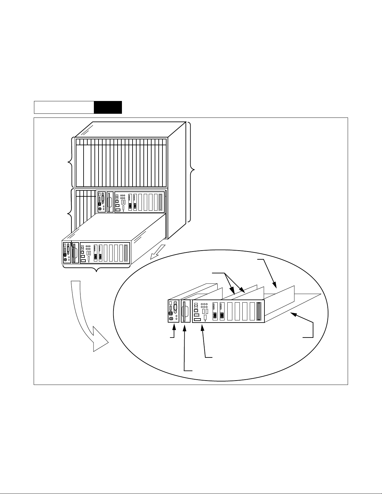
Mounting Location of Circuit Card
2. Mounting Location of Circuit Card
The control circuit cards for the 1 IMG system should be mounted in their dedicated slots, as shown in Figure
1-1. The control circuit cards for the 4 IMG system should be mounted in their dedicated slots, as shown in
Figure 1-2 through Figure 1-2. The control circuit cards for the IMX-U system should be mounted in their
dedicated slots as shown in Figure 1-3 through Figure 1-3.
As a general rule, the blue pull tab line/trunk circuit cards are mounted in the universal slots that are located in
Slots 04 - 12 and 15 - 23 of the Port Interface Module (PIM).
The yellow pull tab line/trunk circuit cards (MIS C) are mounte d in Slots 00 - 02 of the LPM.
Additional GT/LANI cards are mounted in the CPR.
CHAPTER 1 ND-70182 (E)
Page 2
Revision 4.0
PIM3
PIM2
INTRODUCTION
Mounting Location of Circuit Car d
00 01 02 03 04 05 06 07 08 09 10 11 12 13 14 15 16 17 18 19 20 21 22 23
PA-PW55-A(PWR)
PA-PW54-A(DPWR)
00 01 02 03 04 05 06 07 08 09 10 11 12 13 14 15 16 17 18 19 20 21 22 23
PA-PW55-A(PWR)
PA-PW54-A(DPWR)
00 01 02 03 04 05 06 07 08 09 10 11 12 13 14 15 16 17 18 19 20 21 22 23
PA-PW55-A(PWR)
PA-PW54-A(DPWR)
PH-PC36(MUX)
PH-PC36(MUX)
PH-PC36(MUX)
PH-PC36(MUX)
PH-PC36(MUX)
PH-PC36(MUX)
BSCM
PIM1
PIM0
LPM
00 01 02 03 04 05 06 07 08 09 10 11 12 13 14 15 16 17 18 19 20 21 22 23
PA-PW55-A(PWR)
PA-PW54-A(DPWR)
00 01 02 03 04
PH-PC40(EMA)
PH-IO24(IOC)
(IOC/MISC)
(MISC)
(MISC)
PH-SW10(TSW)
PH-SW10(TSW)
Figure 1-1 Card Mounting Slot for the 1 IMG System
ND-70182 (E) CHAPTER 1
Page 3
Revision 4.0
INTRODUCTION
Mounting Location of Circuit Card
NEAX2400IMS(IMX)
4IMG-SYSTEM
IMG0
00 01 02 03 04 05 06 07 08 09 10 11 12 13 14 15 16 17 18 19 20 21 22 23
PA-PW55-A(PWR0)
PA-PW54-A(PWR1)
PIM3
00 01 02 03 04 05 06 07 08 09 10 11 12 13 14 15 16 17 18 19 20 21 22 23
PA-PW55-A(PWR0)
PA-PW54-A(PWR1)
PIM2
00 01 02 03 04 05 06 07 08 09 10 11 12 13 14 15 16 17 18 19 20 21 22 23
PA-PW55-A(PWR0)
PA-PW54-A(PWR1)
PIM
PIM
PIM
B
PIM
S
C
LPM
M
IMG0
PIM
PIM
PIM
PIM
TSWM
IMG1
PH-PC36(MUX)
PH-PC36(MUX)
PH-PC36(MUX)
PH-PC36(MUX)
PH-PC36(MUX)
PH-PC36(MUX)
PIM
PIM
PIM
PIM
Dummy/APM
IMG2
PIM
PIM
PIM
PIM
Dummy/APM
IMG3
BSCM
PIM1
00 01 02 03 04 05 06 07 08 09 10 11 12 13 14 15 16 17 18 19 20 21 22 23
PA-PW55-A(PWR0)
PA-PW54-A(PWR1)
PIM0
00 01 02 03 04
(IOC/MISC)
(MISC)
(MISC)
LPM
PH-PC40(EMA)
PH-IO24(IOC)
PH-PC36(MUX)
PH-PC36(MUX)
Figure 1-2 Card Mounting Slot for the 4 IMG System (1/4)
CHAPTER 1 ND-70182 (E)
Page 4
Revision 4.0
INTRODUCTION
Mounting Location of Circuit Car d
NEAX2400IMS(IMX)
4IMG-SYSTEM
IMG1
00 01 02 03 04 05 06 07 08 09 10 11 12 13 14 15 16 17 18 19 20 21 22 23
PA-PW55-A(PWR0)
PA-PW54-A(PWR1)
PIM3
00 01 02 03 04 05 06 07 08 09 10 11 12 13 14 15 16 17 18 19 20 21 22 23
PA-PW55-A(PWR0)
PA-PW54-A(PWR1)
PIM2
00 01 02 03 04 05 06 07 08 09 10 11 12 13 14 15 16 17 18 19 20 21 22 23
PA-PW55-A(PWR0)
PA-PW54-A(PWR1)
PIM
PIM
PIM
B
PIM
S
C
LPM
M
IMG0
PIM
PIM
PIM
PIM
TSWM
IMG1
PH-PC36(MUX)
PH-PC36(MUX)
PH-PC36(MUX)
PH-PC36(MUX)
PH-PC36(MUX)
PH-PC36(MUX)
PIM
PIM
PIM
PIM
Dummy/APM
IMG2
PIM
PIM
PIM
PIM
Dummy/APM
IMG3
PIM1
PIM0
TSWM
00 01 02 03 04 05 06 07 08 09 10 11 12 13 14 15 16 17 18 19 20 21 22 23
PA-PW55-A(PWR0)
PA-PW54-A(PWR1)
00 01 02 03 04 05 06 07 08 09 10 11 12 13 14 15 16 17 18 19 20 21 22 23
PH-PW14(PWRSW)
PH-PW14(PWRSW)
(MISC)
(MISC)
(MISC)
(MISC)
(MISC)
(MISC)
PH-PC20(DLKC0)
PH-PC20(DLKC1)
PH-GT09(GT0)
PH-PC36(MUX)
PH-PC36(MUX)
PH-GT09(GT1)
PH-SW12(TDSW00)
PH-SW12(TDSW01)
PH-SW12(TDSW02)
PH-SW12(TDSW03)
PH-SW12(TDSW10)
PH-SW12(TDSW11)
Figure 1-2 Card Mounting Slot for the 4 IMG System (2/4)
PH-SW12(TDSW12)
PH-SW12(TDSW13)
PH-CK16/17(PLO0)
PH-CK16/17(PLO1)
ND-70182 (E) CHAPTER 1
Page 5
Revision 4.0
INTRODUCTION
Mounting Location of Circuit Card
NEAX2400IMS(IMX)
4IMG-SYSTEM
IMG2
00 01 02 03 04 05 06 07 08 09 10 11 12 13 14 15 16 17 18 19 20 21 22 23
PA-PW55-A(PWR0)
PA-PW54-A(PWR1)
PIM3
00 01 02 03 04 05 06 07 08 09 10 11 12 13 14 15 16 17 18 19 20 21 22 23
PA-PW55-A(PWR0)
PA-PW54-A(PWR1)
PIM2
00 01 02 03 04 05 06 07 08 09 10 11 12 13 14 15 16 17 18 19 20 21 22 23
PA-PW55-A(PWR0)
PA-PW54-A(PWR1)
PIM
PIM
PIM
B
PIM
S
C
LPM
M
IMG0
PIM
PIM
PIM
PIM
TSWM
IMG1
PH-PC36(MUX)
PH-PC36(MUX)
PH-PC36(MUX)
PH-PC36(MUX)
PH-PC36(MUX)
PH-PC36(MUX)
PIM
PIM
PIM
PIM
Dummy/APM
IMG2
PIM
PIM
PIM
PIM
Dummy/APM
IMG3
PIM1
PIM0
Dummy/APM
00 01 02 03 04 05 06 07 08 09 10 11 12 13 14 15 16 17 18 19 20 21 22 23
PA-PW55-A(PWR0)
PA-PW54-A(PWR1)
00 01 02 03 04 05 06 07 08 09 10 11 12 13 14 15 16 17 18 19 20 21 22 23
PH-PC36(MUX)
PH-PC36(MUX)
Figure 1-2 Card Mounting Slot for the 4 IMG System (3/4)
CHAPTER 1 ND-70182 (E)
Page 6
Revision 4.0
INTRODUCTION
Mounting Location of Circuit Car d
NEAX2400IMS(IMX)
4IMG-SYSTEM
IMG3
00 01 02 03 04 05 06 07 08 09 10 11 12 13 14 15 16 17 18 19 20 21 22 23
PA-PW55-A(PWR0)
PA-PW54-A(PWR1)
PIM3
00 01 02 03 04 05 06 07 08 09 10 11 12 13 14 15 16 17 18 19 20 21 22 23
PA-PW55-A(PWR0)
PA-PW54-A(PWR1)
PIM2
00 01 02 03 04 05 06 07 08 09 10 11 12 13 14 15 16 17 18 19 20 21 22 23
PA-PW55-A(PWR0)
PA-PW54-A(PWR1)
PIM
PIM
PIM
B
PIM
S
C
LPM
M
IMG0
PIM
PIM
PIM
PIM
TSWM
IMG1
PH-PC36(MUX)
PH-PC36(MUX)
PH-PC36(MUX)
PH-PC36(MUX)
PH-PC36(MUX)
PH-PC36(MUX)
PIM
PIM
PIM
PIM
Dummy/APM
IMG2
PIM
PIM
PIM
PIM
Dummy/APM
IMG3
PIM1
PIM0
Dummy/APM
00 01 02 03 04 05 06 07 08 09 10 11 12 13 14 15 16 17 18 19 20 21 22 23
PA-PW55-A(PWR0)
PA-PW54-A(PWR1)
00 01 02 03 04 05 06 07 08 09 10 11 12 13 14 15 16 17 18 19 20 21 22 23
PH-PC36(MUX)
PH-PC36(MUX)
Figure 1-2 Card Mounting Slot for the 4 IMG System (4/4)
ND-70182 (E) CHAPTER 1
Page 7
Revision 4.0
INTRODUCTION
Mounting Location of Circuit Card
NEAX2400IMX
IMX-U SYSTEM
ISW
ISWM
LPM
ISW
PIM
PIM
PIM
PIM
LPM
IMG0
PIM
PIM
PIM
PIM
TSWM0
IMG1
LN 4 (0 3)
ISW
TOPU
00 01 02 03 04 05 06 07 08 09 10 11 12 13 14 15 16 17 18 19
PWR1 (PH-PW14)
PWR0 (PH-PW14)
HSW00 (PU-SW01)(RES)
HSW01 (PU-SW01)
TSW00 (PU-SW00)
TSW01 (PU-SW00)
TSW02 (PU-SW00)
TSW03 (PU-SW00)
IOGT0 (PH-GT10)
IOGT1 (PH-GT10)
PLO0
(PH-CK16-A/17-A)
PLO1
(PH-CK16-A/17-A)
TSW10 (PU-SW00)
ISWM
LANI(PZ-PC19) LANI(PZ-PC19)
00 01 02 03 04
EMA(PH-PC40)
MMC(PH-M22)
IOC(PH-IO24)
Note
I
O
LANI(PZ-PC19) LANI(PZ-PC19)
PIM
PIM
PIM
PIM
TSWM1
IMG2
TSW11 (PU-SW00)
TSW12 (PU-SW00)
TSW13 (PU-SW00)
PWR(PZ-PW106) PWR(PZ-PW106)
LANI(PZ-PC19) LANI(PZ-PC19)
Dummy
HSW10 (PU-SW01)
HSW11 (PU-SW01)(RES)
ISAGT(PZ-GT13) ISAGT(PZ-GT13)
PIM
PIM
PIM
PIM
IMG3
Note:
LPN
BASEU
I
O
PWR
FDD/HDD
DSP
The 2nd IOC card (optional) may be mounted in the slot.
Figure 1-3 Card Mounting Slot for the IMX-U System (1/5)
CHAPTER 1 ND-70182 (E)
Page 8
Revision 4.0
INTRODUCTION
Mounting Location of Circuit Car d
NEAX2400IMX
IMX-U SYSTEM
ISWM
IMG0
00 01 02 03 04 05 06 07 08 09 10 11 12 13 14 15 16 17 18 19 20 21 22 23
PA-PW55-A (PWR0)
PA-PW54-A (PWR1)
PIM3
00 01 02 03 04 05 06 07 08 09 10 11 12 13 14 15 16 17 18 19 20 21 22 23
PA-PW55-A (PWR0)
PA-PW54-A (PWR1)
PIM2
00 01 02 03 04 05 06 07 08 09 10 11 12 13 14 15 16 17 18 19 20 21 22 23
PA-PW55-A (PWR0)
PA-PW54-A (PWR1)
LPM
ISW
PIM
PIM
PIM
PIM
LPM
IMG0
PH-PC36 (MUX)
PH-PC36 (MUX)
PH-PC36 (MUX)
PIM
PIM
PIM
PIM
TSWM0
IMG1
LN 4 (0 3)
PH-PC36 (MUX)
PH-PC36 (MUX)
PH-PC36 (MUX)
PIM
PIM
PIM
PIM
TSWM1
IMG2
PIM
PIM
PIM
PIM
Dummy
IMG3
BSCM
PIM1
00 01 02 03 04 05 06 07 08 09 10 11 12 13 14 15 16 17 18 19 20 21 22 23
PA-PW55-A (PWR0)
PA-PW54-A (PWR1)
PIM0
LPM
00 01 02 03 04
PH-M22(MMC)
(MISC)
PH-PC40(EMA)
PH-IO24(IOC)
(IOC/MISC)
PH-PC36 (MUX)
PH-PC36 (MUX)
Figure 1-3 Card Mounting Slot for the IMX-U System (2/5)
ND-70182 (E) CHAPTER 1
Page 9
Revision 4.0
INTRODUCTION
Mounting Location of Circuit Card
IMX-U SYSTEM
PIM3
PIM2
NEAX2400IMX
IMG1
PA-PW55-A (PWR0)
PA-PW55-A (PWR0)
PA-PW54-A (PWR1)
PA-PW54-A (PWR1)
ISWM
LPM
ISW
PIM
PIM
PIM
PIM
LPM
IMG0
PH-PC36 (MUX)
PH-PC36 (MUX)
PH-PC36 (MUX)
PH-PC36 (MUX)
PIM
PIM
PIM
PIM
TSWM0
IMG1
TSWM1
LN 4 (0 3)
PIM
PIM
PIM
PIM
IMG2
21 22 23201918171615141312111009080706050403020100
21 22 23201918171615141312111009080706050403020100
PIM
PIM
PIM
PIM
Dummy
IMG3
PIM1
PIM0
TSWM0
PA-PW55-A (PWR0)
PA-PW54-A (PWR1)
PA-PW55-A (PWR0)
PA-PW54-A (PWR1)
PH-PW14 (PWRSW)
PH-PW14 (PWRSW)
(MISC)
(MISC)
(MISC)
(MISC)
(MISC)
PH-PC20 (DLKC0)
PH-PC20 (DLKC1)
(MISC)
PH-GT09 (GT0)
PH-PC36 (MUX)
PH-PC36 (MUX)
PH-PC36 (MUX)
PH-PC36 (MUX)
PH-GT09 (GT1)
PH-SW12 (TSW00)
PH-SW12 (TSW01)
PH-SW12 (TSW02)
PH-SW12 (TSW03)
PH-SW12 (TSW10)
PH-SW12 (TSW11)
PH-SW12 (TSW12)
PH-SW12 (TSW13)
21 22 23201918171615141312111009080706050403020100
21 22 23201918171615141312111009080706050403020100
21 22 23201918171615141312111009080706050403020100
PH-CK16-A/17-A (PLO1)
PH-CK16-A/17-A (PLO0)
Figure 1-3 Card Mounting Slot for the IMX-U System (3/5)
CHAPTER 1 ND-70182 (E)
Page 10
Revision 4.0
INTRODUCTION
Mounting Location of Circuit Car d
IMX-U SYSTEM
PIM3
PIM2
NEAX2400IMX
IMG2
PA-PW55-A(PWR0)
PA-PW55-A(PWR0)
PA-PW54-A(PWR1)
PA-PW54-A(PWR1)
ISWM
LPM
ISW
PIM
PIM
PIM
PIM
LPM
IMG0
PH-PC36(MUX)
PH-PC36(MUX)
PH-PC36(MUX)
PH-PC36(MUX)
PIM
PIM
PIM
PIM
TSWM0
IMG1
LN 4 (0 3)
PIM
PIM
PIM
PIM
TSWM1
IMG2
21 22 23201918171615141312111009080706050403020100
21 22 23201918171615141312111009080706050403020100
PIM
PIM
PIM
PIM
Dummy
IMG3
PIM1
PIM0
TSWM1
PA-PW55-A(PWR0)
PA-PW54-A(PWR1)
PA-PW55-A(PWR0)
PA-PW54-A(PWR1)
PH-PW14 (PWRSW0)
PH-PW14 (PWRSW1)
PH-PC36(MUX)
PH-PC36(MUX)
PH-GT09 (GT0)
PH-GT09 (GT1)
PH-SW12 (TSW00)
PH-SW12 (TSW01)
PH-PC36(MUX)
PH-PC36(MUX)
PH-SW12 (TSW02)
PH-SW12 (TSW03)
PH-SW12 (TSW10)
PH-SW12 (TSW11)
PH-SW12 (TSW12)
21 22 23201918171615141312111009080706050403020100
21 22 23201918171615141312111009080706050403020100
21 22 23201918171615141312111009080706050403020100
PH-SW12 (TSW13)
PH-CK18 (CLK0)
PH-CK18 (CLK1)
Figure 1-3 Card Mounting Slot for the IMX-U System (4/5)
ND-70182 (E) CHAPTER 1
Page 11
Revision 4.0

INTRODUCTION
Mounting Location of Circuit Card
IMX-U SYSTEM
PIM3
PIM2
NEAX2400IMX
IMG3
PA-PW55-A(PWR0)
PA-PW55-A(PWR0)
PA-PW54-A(PWR1)
PA-PW54-A(PWR1)
ISWM
LPM
ISW
PIM
PIM
PIM
PIM
LPM
IMG0
PH-PC36(MUX)
PH-PC36(MUX)
PH-PC36(MUX)
PH-PC36(MUX)
PIM
PIM
PIM
PIM
TSWM0
IMG1
TSWM1
LN 4 (0 3)
PIM
PIM
PIM
PIM
IMG2
21 22 23201918171615141312111009080706050403020100
21 22 23201918171615141312111009080706050403020100
PIM
PIM
PIM
PIM
Dummy
IMG3
PIM1
PIM0
Dummy
PA-PW55-A(PWR0)
PA-PW54-A(PWR1)
PA-PW55-A(PWR0)
PA-PW54-A(PWR1)
PH-PC36(MUX)
PH-PC36(MUX)
PH-PC36(MUX)
PH-PC36(MUX)
21 22 23201918171615141312111009080706050403020100
21 22 23201918171615141312111009080706050403020100
Figure 1-3 Card Mounting Slot for the IMX-U System (5/5)
CHAPTER 1 ND-70182 (E)
Page 12
Revision 4.0

CHAPTER 2 CONTROL CIRCUIT CARD REFERENCE
This chapter ex plains the following items fo r each Control C ircuit Card.
• General Function
Explains the general function and purpose of each control circuit card.
• Mounting Location/Condition
Explains the mounting loca tion (mounting module name and slot number , etc.) fo r each circuit card. If there
are any conditions pertaining to mounting the circuit cards, they are also explained.
• Face Layout of Lamps, Switches, and Connectors
The locations of the lamps, switche s, and conne ctors pro vided on ea ch circu it car d are illust rate d by a fac e
layout.
• Lamp Indications
The names, colors, and indication states of lamps mounted on each circuit card are listed.
• Switch Settings
Each circuit card's switches are listed with their names, switch numbers, their setting and its meaning,
standard setting, etc.
• External Inte rface
If the lead outputs of the circuit card are provided by an LT connector, the relation between the mounting
slots and the LT connectors is illustrated by an LT Connector Lead Face Layout. If the lead outputs are
provided by other than an LT connector, or are provided by the circuit card front connector, the connector
lead locations and the connecting routes are shown.
In addition, a Switch Setting Sheet, which may be used to record the switch settings, is provided at the end of
the explanation for each circ uit card.
ND-70182 (E) CHAPTER 2
Page 13
Revision 4.0
SN1374 CPRP-A
CPU Board
SN1374 CPRP-A
CPU Board
1. General Function
The Central Pr o cessing Rack ( CPR) consists o f the following components.
(a) CPU BOARD: Contains the Main Processor Unit (MPU), R OM, a nd 128 Mbyte of Random Acces s
(b) DSP: Contains the CPR switches and the CPR status indicator lamps.
(c) FDD/HDD: Floppy Disk Drive (FDD) and Hard Disk Drive (HDD) are mounted on a circuit
(d) PWR: Supplies the operating power to the CPR, and also the MISC slots of the LPM.
Memory (RAM). Also, this board may be equipped with the ISAGT (PZ-GT16) on
its Industrial St andard Architecture (ISA) and LANI (PZ-PC19) on the Peripheral
Component Interconnect (PCI).
card, which can be extracted and/or inserted while the system is in operation, if
required.
To HUB
To HUB
To I/O local bus
LANI
DSP
CPULANI
CPR#0
ISAGT ISAGT
To MISC bus
DSP
CPU LANI
CPR#1
LANI
Figure 2-1 Location of SN1374 CPRP-A (CPR) in the System
To HUB
To HUB
CHAPTER 2 ND-70182 (E)
Page 14
Revision 4.0
SN1374 CPRP-A
CPU Board
2. Mounting Location/Condition
The CPR is composed of a CPU BO ARD, DSP, FDD/HDD and PWR, and is l ocated in the Loca l Processor
Module (LPM) as shown below. Since the CPR provides the Industry Standard Architecture (ISA) bus and
Peripheral Component Interconnect (PCI) bus, the GT and LANI cards are located in those busses
respectively.
Mounting Module
PIM0
LPM
CPR
LPM
BSCM
PZ-GT16 (ISAGT)
PZ-PC19 (LANI)
PZ-PW92 (PWR)
Figure 2-2 CPR Location
PT-2200 (CPU BOARD)
PZ-DK224 (DSP)
PZ-IO27(FDD/HDD)
ND-70182 (E) CHAPTER 2
Page 15
Revision 4.0
SN1374 CPRP-A
CPU Board
3. Face Layout of Lamps, Switches and Connectors
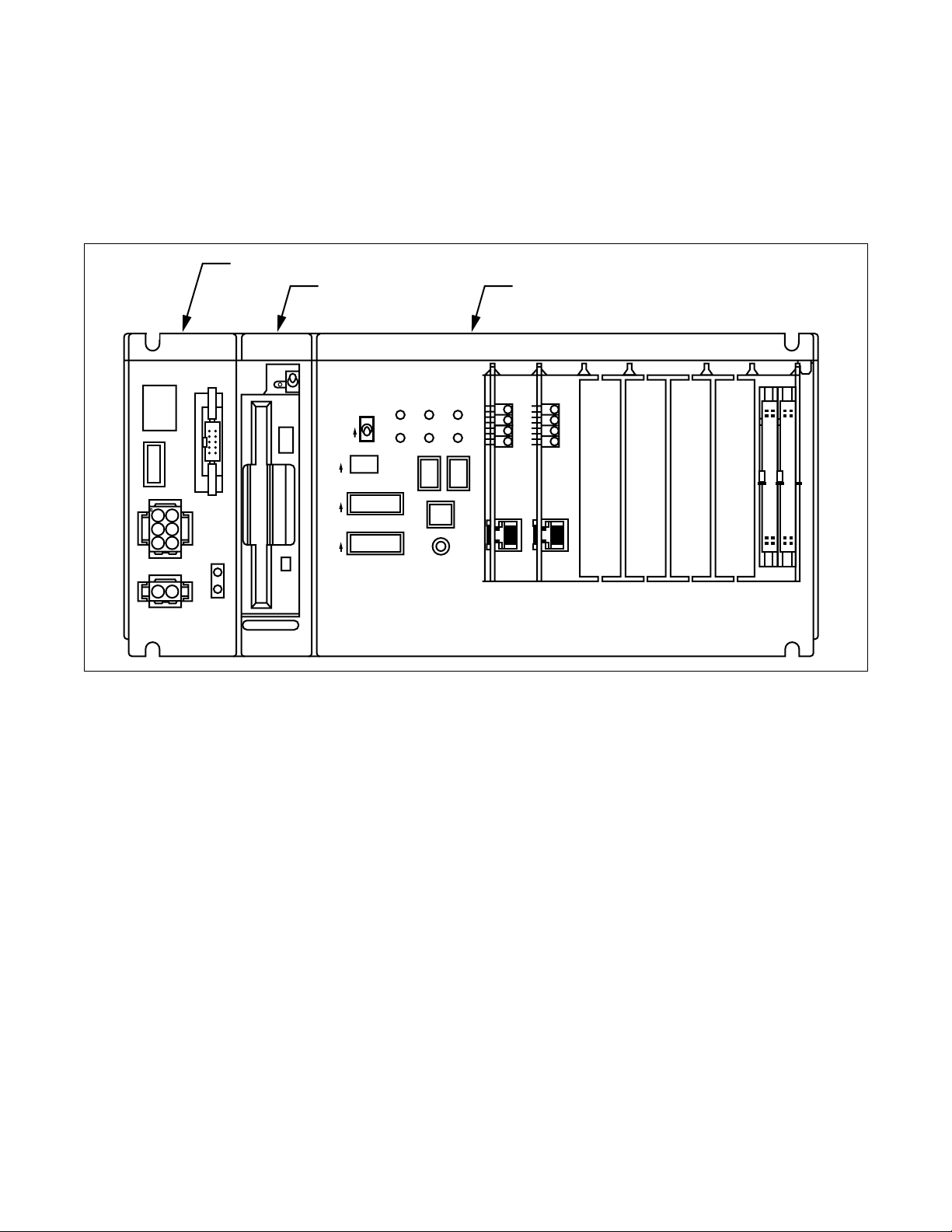
The CPR has the following lamps, switches and connectors.
Slot numbers 0-3 provide the Peripheral Component Interconnect (PCI) bus, and slot numbers 4-6 are the
Industrial Standard Architecture (ISA) bus.
PWR (PZ-PW92)
FDD/HDD (PZ-IO27) DSP (PZ-DK224)
PZ-PW92
DC-40V~-58.6V
SW
I
O
-48V OUT
OUTPWR
INPWR
ON
OFF
5A
125V
AC/DC
PALM
ON
ALM
HDD
CPU OPE
MBR
ON
GT1
SYSTEM SELECT0 STATUS
ON
14
SYSTEM SELECT1
ON
112
SYSTEM SELECT2
ON
13 20
WDT
GT0
GT2
GT3
SENSE
CPURST
SLOT NO. 0 1 2 3 4 5 6
AB
Figure 2-3 Front View of CPR
CHAPTER 2 ND-70182 (E)
Page 16
Revision 4.0

4. Lamp Indications
LAMP NAME COLOR DESCRIPTION
ON (PWR) Green Lights green when the PWR is supplied.
ALM (PWR) Red Lights red when the PWR is abnormal.
HDD
(HDD)
Red Lights red while the HDD is being accessed.
SN1374 CPRP-A
CPU Board
WDT
(DSP)
CPU OPE
(DSP)
IMG0
(DSP)
IMG1 (DSP) Green Not used.
IMG2 (DSP) Green Not used
IMG3 (DSP) Green Not used
Red Lights red when Watch-dog Timer (WD T) time-out has occurred.
Green Lights green when the CPU is in active state.
Lights green when PZ-GT16 (located in Slot 6) is in active state.
Green
Flashes green when PZ-GT16 (located in Slot 6) is in stand-by state
ND-70182 (E) CHAPTER 2
Page 17
Revision 4.0

SN1374 CPRP-A
CPU Board
LAMP
NAME
STATUS
(DSP)
DESCRIPTION
Two sets of “7-segment LED” show the CPR processing status. The CPR processing status is determined by
the Sense switch settings, and the new processing status starts when the CPURST button is pressed. The 7segment LED indication on each CPR processing status is listed belo w.
SENSE
1
2
3 Not used “c” “c” indicated when copying the dat a from FD to HD
4 Not used “d” “d” indicated whil e mak i ng the directory on the HD
STATUS
LEFT RIGHT
“F”
Not used
Not used “1”
“0-9” “0-9”
Not used
Not used
“c”
“d”
“S”
“b”
“y”
“1”
1. When Program Install
The HD in the CPR initializes and the program installs. (These processes
execute)
“F” indicated during HD format.
“c” indicated when copyin g dat a from FD
“d” indicated while creating the directory on the HD
2. When Program Load
After program installation, th e prog ram should b e transferre d from the HD to
the memory.
“1” indicated during this process.
3. On-line active CPR
The active CPR in ON LINE status indi cate s th e CPU occupanc y rate in
percentages (00-99%)
4. On-line stand-by CPR
The stand-by CPR in ON LINE status indicates “S,” “b,” “y”
5. Program & Office data load
“0”
“1” indicated during the Program and Office data transfer from the HD to
memory
“0” indicated during the Office data load.
DESCRIPTION
The CPR is starting-up with ON LINE (OAI memory clear restart).
5 Not used
6 Not used “F” “F” indi cated during HD format.
C N ot used “H”
“1”
“0”
“1” indicated during the Program load.
“0” indicated during the process.
The CPR is starting-up with OFF LINE.
“H” indicated during the ROM data loading.
Note:
The segment spinning indication shows a processing status has completed successfully, or “E” means the
processing failed.
Segment Spinning Indication
CHAPTER 2 ND-70182 (E)
Page 18
Revision 4.0

5. Switch Settings
SN1374 CPRP-A
CPU Board
SWITCH
NAME
SW
(PWR)
MB Note
(FDD/HDD)
MBR
(DSP)
CPURST — —
SYSTEM
SELECT0
(DSP)
SWITCH
NO.
—
—
—
1OFF × Not used
2OFF × Not used
3OFF × Not used
4
1
SETTING
ON (Up) Make-busy of the FDD/HDD.
OFF (Down) × Normal setting
ON (Up)
OFF (Down) × Normal setting
STANDARD
SETTING
ON × PWR is supplied to the CPR.
OFF PWR is not supplied to the CPR.
Make-busy Request of the CPR in which GT is
located.
Execute the CPR processing according to the
SENSE setting.
ON Watchdog Timer time-out is not detected.
OFF × Watchdog Timer time-out is detected.
ON PCI Card (Slot 0) MBR ON
OFF PCI Card (Slot 0) MBR OFF
MEANING
SYSTEM
SELECT1
SYSTEM
SELECT2
Note:
2
ON PCI Card (Slot 1) MBR ON
OFF PCI Card (Slot 1) MBR OFF
ON PCI Card (Slot 2) MBR ON
OFF PCI Card (Slot 2) MBR OFF
ON PCI Card (Slot 3) MBR ON
(DSP)
3
4
OFF PCI Card (Slot 3) MBR OFF
5~8 OFF × Fixed to “OFF.”
1~8 OFF × Not used
(DSP)
Make-busy of this circuit card is not allowed while the Floppy Disk Drive or Hard Disk Drive is being
accessed.
ND-70182 (E) CHAPTER 2
Page 19
Revision 4.0

SN1374 CPRP-A
CPU Board
SWITCH
NAME
SENSE
Note
Note:
The SENSE switch designates the CPR processing status. The new processing status starts when the
CPRRST switch on the DSP is pressed while setting the SENSE switch.
6. External Interface
See the NEAX2400 IMX Installation Manual.
SETTING
STANDARD
SETTING
MEANING
The following three processes are executed at the FDD/HDD.
1
• HD format
• File copied from FDD to HD
• Directory created on the HD
2 On-line mode
3 File copied from FDD to HD in the FDD/HD
4 The directory created on the HD of the FDD/HDD
5
OAI memory cleared, and the CPR started up in ON LINE mode b y
loading the ROM data
6 HD format of the FDD/HDD
C The CPR starts up in OFF LINE mode by loading the ROM data.
7. Switch Setting Sheet
SWITCH NAME SWITCH S HAPE REMARKS
SW
(PWR)
MB
(FDD/HDD)
MBR
(DSP)
NMI-SEL
SYSTEM
SELECT0
(DSP)
1 2 3
ON
OFF
ON
ON
ON
ON
4
CHAPTER 2 ND-70182 (E)
Page 20
Revision 4.0

SWITCH NAME SWITCH S HAPE REMARKS
SN1374 CPRP-A
CPU Board
SYSTEM
SELECT1
(DSP)
SYSTEM
SELECT2
(DSP)
SENSE
(DSP)
1 2 3
1
2 3
4
4
5 6 7
5
6 7
ON
8
ON
8
ND-70182 (E) CHAPTER 2
Page 21
Revision 4.0

SN1401 CPRAC-A
CPU Board
SN1401 CPRAC-A
CPU Board
1. General
The CPR consists of the following components.
(a) CPU BOARD: Contains the Main Processor Unit (MPU), R OM, a nd 128 Mbyte of Random Acces s
(b) DSP: Contains the CPR switches and the CPR status indicator lamps.
(c) FDD/HDD: Floppy Disk Drive (FDD) and Hard Disk Drive (HDD) are mounted on a circuit
(d) PWR: Supplies the operating power to the CPR and also the MISC slots of the LPM.
Memory (RAM). Additionally, this board may be equipped with the ISAGT (PZGT13) on its Industrial Standard Architecture (ISA) bus, and LANI (PZ-PC19) on
the Peripheral Component Interconnect (PCI).
card, which can be extracted and/or inserted while the system is in operation, if
necessary.
To HUB
To HUB
To I/O loc al bus
DSP
CPU
LANI
LANI
LANI
LANI
DSP
CPU
ISAGT
To MISC bus
ISAGT
Figure 2-4 Location of SN1401 CPRAC-A (CPR) in the System
To HUB
To HUB
CHAPTER 2 ND-70182 (E)
Page 22
Revision 4.0

SN1401 CPRAC-A
CPU Board
2. Mounting Location/Condition
The CPR is composed of the CPU BOARD, DSP, FDD/HDD, and PWR and is located in the Local
Processor Module (LPM) as shown below. Since the CPR provides the Industrial Standard Architecture
(ISA) bus and Peripheral Component Interconnect (PCI) bus, the GT and LANI cards are located in those
busses respectively.
PIM0
BSCM
LPM
CPR
PZ-PC19 (LANI)
PZ-PW92 (PWR)
PZ-GT13 (ISAGT)
CPU BOARD
PZ-DK224 (DSP)
PZ-IO27(FDD/HDD)
Figure 2-5 CPR Location
ND-70182 (E) CHAPTER 2
Page 23
Revision 4.0

SN1401 CPRAC-A
CPU Board
3. Face Layout of Lamps, Switches, and Connectors
The CPR has the following lamps, switches and connectors.
Slots 0-3 provide the Peripheral Component Interconnect (PCI) bus, and Slots 4-6 are the Industrial
Standard Architecture (ISA) bus.
PWR(PZ-PW92)
FDD/HDD(PZ-IO27) DSP(PZ-DK224)
PZ-PW92
DC-40V~-58.6V
SW
I
O
-48V OUT
OUTPWR
INPWR
ON
OFF
5A
125V
AC/DC
PALM
ON
ALM
HDD
CPU OPE
MBR
ON
IMG1
SYSTEM SELECT0 STATUS
ON
14
SYSTEM SELECT1
ON
112
SYSTEM SELECT2
ON
13 20
WDT
IMG0
IMG2
IMG3
SENSE
CPURST
SLOT NO. 0 1 2 3 4 5 6
AB
Figure 2-6 Front View of CPR
4. Lamp Indications
LAMP NAME COLOR DESCRIPTION
ON (PWR) Green Lights green when the PWR is supplied.
ALM (PWR) Red Lights red when the PWR is abnormal.
HDD
(FDD/HDD)
WDT (DSP) Red Lights red when Watch-dog Timer (WDT) time-out has occurs.
CPU OPE (DSP) Green Lights green when the CPU is in active state.
IMG0 (DSP) Green
IMG1 (DSP) Green Flashes green when IMG1 is mounted. Note
IMG2 (DSP) Green Flashes green when IMG2 is mounted. Note
IMG3 (DSP) Green Flashes green when IMG3 is mounted. Note
Note:
No lamp indication in STBY mode.
Red Lights red while the HDD or FDD is being accessed.
Lights green when PZ-GT13 (located in Slot 6) is in active state.
Flashes green when PZ-GT13 (located in Slot 6) is in stand-by state.
CHAPTER 2 ND-70182 (E)
Page 24
Revision 4.0

SN1401 CPRAC-A
CPU Board
LAMP
NAME
STATUS
(DSP)
DESCRIPTION
T w o set of “7-segment LED” sho ws the CPR processing status. The CPR processing status is determined by the
SENSE switch settin gs, and the new process ing status starts when t he CPURST switch is press ed. The 7-segment
LED indication on each CPR processing status is listed below.
SENSE
1
2
3 Not used “c” “c” indicated during copy the data from FD to HD
4 Not used “d” “d” indicated while making the directory on the HD
5 Not used
6 Not used “F” “F” indicated during HD format.
C Not used “H”
STATUS
LEFT RIGHT
“F”
Not used
Not used “1”
“0-9” “0-9”
Not used
Not used
“c”
“d”
“S”
“b”
“y”
“1”
“1”
1. When Program Install
The HD in the CPR initializes and the program is installed. (These processes ex-
ecute)
“F” indicated during HD format.
“c” indicated when copying the data from FD to HD
“d” indicated while creating the directory on the HD
2. When Program Load
After the program installation, the program should b e transferred from the HD to
the memory.
“1” indicated during this process.
3. On-line active CPR
The active CPR which is in ON LINE status indicates the CPU occupancy rate in
percentages. (00-99%)
4. On-line stand-by CPR
The stand-by CPR which is in ON LINE status indicates “S,” “b,” “y”
5. Program & Office data load
“0”
“0”
“1” indicated during the Program and Office data transferred from the HD to
the memory
“0” indicated during the Office data load
The CPR is starting-up with ON LINE (OAI memory clear restart).
“1” indicated during the Program load.
“0” indicated during the process.
The CPR is starting-up with OFF LINE.
“H” indicated during the ROM data loading.
DESCRIPTION
Note:
The segme nt spinni ng indi cation shows a processing status has completed successful ly, or else “E” means
the processing failed.
Segment Spinning Indication
ND-70182 (E) CHAPTER 2
Page 25
Revision 4.0

SN1401 CPRAC-A
CPU Board
5. Switch Settings
SWITCH NAME
SW
(PWR)
Note
MB
(FDD/HDD)
MBR
(DSP)
CPURST — —
SYSTEM
SELECT0
(DSP)
SWITCH
NO.
—
—
—
1OFF × Not used
2OFF × Not used
3OFF × Not used
4
1
SETTING
ON × PWR is supplied to the CPR.
OFF PWR is not supplied to the CPR.
ON (Up) Make-busy of the FDD/HDD.
OFF (Down) × Normal setting.
ON (Up)
OFF (Down) × Normal setting.
ON Watchdog Timer time-out is not detected.
OFF × Watchdog Timer time-out is detected.
ON PCI Card (Slot 0) MBR ON
OFF PCI Card (Slot 0) MBR OFF
STANDARD
SETTING
MEANING
Make-busy Request of the CPR in which the
GT is located.
Execute the CPR processing according to the
SENSE setting.
Note:
ON PCI Card (Slot 1) MBR ON
OFF PCI Card (Slot 1) MBR OFF
ON PCI Card (Slot 2) MBR ON
OFF PCI Card (Slot 2) MBR OFF
ON PCI Card (Slot 3) MBR ON
OFF PCI Card (Slot 3) MBR OFF
SYSTEM
SELECT1
(DSP)
SYSTEM
SELECT2
(DSP)
2
3
4
5~8 OFF × Fixed to “OFF.”
1~8 OFF × Not used
Make-busy of this circuit card is not allowed while the Floppy Disk Drive or Hard Disk Drive is being
accessed.
CHAPTER 2 ND-70182 (E)
Page 26
Revision 4.0

SN1401 CPRAC-A
CPU Board
SWITCH
NAME
SETTING
SENSE
Note
Note:
The SENSE switch designates the CPR processing status. The new processing status starts when the
CPRRST switch on the DSP is pressed while setting the SENSE switch.
6. External Interface
See the NEAX2400 IMX Installation Manual.
STANDARD
SETTING
MEANING
The following three process are executed at the FDD/HDD.
1
• HD format
• File copied from FDD to HD
• Directory created on the HD
2 × On line mode.
3 File copied from FDD to HD within the FDD/HDD.
4 Directory created on the HD of the FDD/HDD.
5
OAI memory clear, and the CPR starts up in ON LINE mode by loading the
ROM data.
6 HD format of the FDD/HDD.
C The CPR starts up in OFF LINE mode by loading the ROM data.
7. Switch Setting Sheet
SWITCH NAME SWITCH SHAPE REMARKS
SW
(PWR)
MB
ON
OFF
ON
(FDD/HDD)
MBR
ON
(DSP)
NMI-SEL
ON
SYSTEM
1
2 3 4
ON
SELECT0
SYSTEM
1
5
2 3
6 7
4
ON
8
SELECT1
SYSTEM
1 2 3
4
5 6 7
ON
8
SELECT2
SENSE
ND-70182 (E) CHAPTER 2
Page 27
Revision 4.0

PH-GT09
Gate
PH-GT09
Gate
1. General Function
The PH-GT09 (GT) circuit card provides both the TSW I/O Local bus and the MISC bus interface. The
CPR controls TSW, PLO, DLKC, and MISC via the ISAGT and GT.
TDSW I/O
Local Bus
PLO0
TDSW03
TDSW02
PLO1
TDSW13
TDSW I/O
Local Bus
TDSW12
TDSW11
To HUB
To HUB
LANI
TDSW01
TDSW00
CPULANI
CPR #0
DLKC0
DSP
ISAGT
MISC Bus
GT
MISC Bus
MISC
EMA
GT
ISAGT
MISC Bus
DLKC1
DSP
TDSW10
CPU
CPR #1
LANI
LANI
To HUB
To HUB
IOC/
MISC
Figure 2-7 Location of PH-GT09 (GT) Card in the System
CHAPTER 2 ND-70182 (E)
Page 28
Revision 4.0
2. Mounting Location/Condition
This circuit card is mounted in the TSWM of the slot shown below.
PH-GT09
Gate
Mounting Module
00 01 02 03 04 05 06 07 08 09
TSWM
10 11 12 13 14 15 16 17 18 19 20 21 22 23
GT1
GT0
3. Face Layout of Lamps, Switches, and Connectors
The face layout of lamps, switches, and connector s is shown in Figure 2-8.
OPE/MB
Figure 2-8 Face Layout of PH-GT09 (GT)
MB
MBR
ND-70182 (E) CHAPTER 2
Page 29
Revision 4.0

PH-GT09
Gate
4. Lamp Indications
Lamp indications for this circuit card are shown in the table below.
LAMP NAME COLOR STATE
OPE/MB Green Remains lit while this circuit card is in ACT state.
5. Switch Settings
Standard settings for switches on this circuit card are shown in the table below.
SWITCH
NAME
MB
MBR
Note
Note:
SETTING
UP Make-busy of circuit card
DOWN × Normal setting
UP
DOWN × Normal setting.
Prior to extracting the GT card, flip the MBR switch on and then flip the MB switch on.
STANDARD
SETTING
MEANING
When the ACT side of GT’s MBR switch is flipped, the ST - BY side of
TSW, DLKC, and GT is forced to switch over the ACT side. (When the
TSW is dual configuration.)
6. External Interface
See the NEAX2400 IMX Installation Manual.
7. Switch Setting Sheet
SWITCH NAME SWITCH SHAPE REMARKS
MB
ON
MBR
CHAPTER 2 ND-70182 (E)
Page 30
Revision 4.0
ON

SN1455 CPRAQ-A/SN1531 CPRAS-A
CPU Board
1. General Function
The CPR consists of the following components.
(a) CPU BOARD: Contains the Main Processor Unit (MPU), R OM, a nd 128 Mbyte of Random Acces s
Memory (RAM). This board may also contain the ISAGT (PZ-GT13/PZ-GT20) on
its Industrial Standard Architecture (ISA) bus, and LANI (PZ-PC19) on the
Peripheral Component Interconnect (PCI).
(b) DSP: Contains the CPR switches and the CPR status indicator lamps.
(c) FDD/HDD: Floppy Disk Drive (FDD) and Hard Disk Drive (HDD) are mounted on a circuit
card, which , if necessar y, can be extracted and/or inserted while the system is in
operation.
(d) PWR: Supplies the operating power to the CPR and also the MISC slots of the LPM.
SN1455 CPRAQ-A/SN1531 CPRAS-A
CPU Board
To HUB
To HUB
To I/O local bus
HDD
FDD
LANI
LANI
Figure 2-9 Location of SN1455 CPRAQ-A/SN1531 CPRAS-A (CPR)
DSP
CPU CPU
CPR#0 CPR#1
ISAGT ISAGT
To MISC bus
DSP
HDD
FDD
LANI
LANI
To HUB
To HUB
ND-70182 (E) CHAPTER 2
Page 31
Revision 4.0

SN1455 CPRAQ-A/SN1531 CPRAS-A
CPU Board
2. Mounting Location/Condition
The CPR is composed of the CPU BOARD, DSP, FDD/HDD, and PWR and is located in the Local
Processor Module (LPM) as shown in Figure 2-10. Since the CPR provides the Industrial Standard
Architecture (ISA) bu s and Perip heral Component Interconne ct (PCI) b us, the ISAGT and LANI cards are
located in those busses respectively.
ISWM/PIM0
LPM
BSCM
Note:
PZ-GT20 (ISAGT) Note
CPR
PZ-PW92 (PWR)
PZ-PC19 (LANI)
PZ-DK224 (DSP)
PZ-IO27(FDD/HDD)
This card is mounted in the IMG0 of the IMX-U system only.
Figure 2-10 CPR Location
PZ-PC19
(LANI)
PZ-GT13
(ISAGT)
CPU BOARD
CHAPTER 2 ND-70182 (E)
Page 32
Revision 4.0

SN1455 CPRAQ-A/SN1531 CPRAS-A
CPU Board
3. Face Layout of Lamps, Switches, and Connectors
The CPR contains the following lamps, switches and connectors.
Slots 0-3 provide the Peripheral Component Interconnect (PCI) bus, and Slots 4-6 are the Industrial
Standard Architecture (ISA) bus.
PWR(PZ-PW92)
FDD/HDD(PZ-IO27) DSP(PZ-DK224)
PZ-PW92
DC-40V~-58.6V
SW
I
O
-48V OUT
OUTPWR
INPWR
5A
125V
AC/DC
ON
OFF
ALM
PALM
ON
HDD
WDT
CPU OPE
MBR
ON
IMG1
IMG2
SYSTEM SELECT0 STATUS
ON
14
SYSTEM SELECT1
ON
112
SYSTEM SELECT2
ON
13 20
SENSE
CPURST
IMG0
IMG3
SLOT NO. 0 1 2 3 4 5 6
AB
Note
Note:
This card is mounted in the IMG0 of the IMX-U sys te m only.
Figure 2-11 Front View of CPR
4. Lamp Indications
Lamp Indications va ry depending on the node. The following shows the lamp indications for the CPR in
the IMG.
LAMP NAME COLOR DESCRIPTION
ON (PWR) Green Lights green when the PWR is supplied.
ALM (PWR) Red Lights red when the PWR is abnormal.
HDD
(FDD/HDD)
WDT (DSP) Red Lights red when Watch-dog Timer (WDT) time-out has occurred.
CPU OPE (DSP) Green Lights green when the CPU is in active state.
CPU OPE (DSP) Green Lights green when the CPU is in active state.
Red Lights red while the HDD or FDD is being accessed.
ND-70182 (E) CHAPTER 2
Page 33
Revision 4.0

SN1455 CPRAQ-A/SN1531 CPRAS-A
CPU Board
LAMP NAME COLOR DESCRIPTION
IMG0 (DSP) Green Flashes green when PZ-GT13 (located in slot number 6) is in operation.
IMG1 (DSP) Green Flashes green when IMG1 is mounted. Note
IMG2 (DSP) Green Flashes green when IMG2 is mounted. Note
IMG3 (DSP) Green Flashes green when IMG3 is mounted. Note
Note:
No lamp indication in STBY mode.
The following shows the lamp indication for the CPR in the ISW
LAMP NAME COLOR DESCRIPTION
ON (PWR) Green Lights green when the PWR is supplied.
ALM (PWR) Red Lights red when the PWR is abnormal.
HDD (FDD/HDD) Red Lights red while the HDD or FDD is being accessed.
WDT (DSP) Red Lights red when Watch-dog Ti mer (WDT) time-out has occu rred.
CPU OPE (DSP) Green Lights green when the CPU of the ISW is in active state.
IMG0 (DSP) Green
IMG1 (DSP) Green Lights green when the TSW1 of the ISW is used. Note
IMG2 (DSP) Green Lights green when the TSW2 of the ISW is used. Note
IMG3 (DSP) Green Lights green when the TSW3 of the ISW is used. Note
Note:
No lamp indication in STBY mode.
Lights green when the CPU of the ISW is in active state.
Flashes green when the CPU of the ISW is in stand-by state.
CHAPTER 2 ND-70182 (E)
Page 34
Revision 4.0

SN1455 CPRAQ-A/SN1531 CPRAS-A
CPU Board
LAMP
NAME
STATUS
(DSP)
DESCRIPTION
Two sets of “7-segment LED” sho w the CPR pro cessing s tatus. The CPR p rocessing status is determined by th e
SENSE switch settin gs, and the new process ing status starts when t he CPURST switch is press ed. The 7-segment
LED indication on each CPR processing status is listed below.
SENSE
1
2
3 Not used “c” “c” indicated when copying the data from FD to HD
4 Not used “d” “d” indicated while making th e dir e c to r y on the HD
5 Not used
6 Not used “F” “F” indicated during HD format.
C Not used “H”
STATUS
LEFT RIGHT
“F”
Not used
Not used “1”
“0-9” “0-9”
Not used
Not used
“c”
“d”
“S”
“b”
“y”
“1”
“1”
1. When Program Install
The HD in the CPR is initialized and the program is installed. (Th ese three
processes execute)
“F” indicated during HD format.
“c” indicated when copying data from FD to HD
“d” indicated while making the directory on the HD
2. When Program Load
After program installation, the program should be transfe rred from th e HD
to memory.
“1” is indicated during this process.
3. On-line active CPR
The active CPR which is in ON LINE status indicates the CPU occupancy
rate by percentage. (00-99%)
4. On-line stand-by CPR
The stand-by CPR which is in ON LINE status indicates “S,” “b,” “y”
5. Program & Office data load
“0”
“0”
“1” indicated during the Program and Office data transfer from the HD to
the memory
“0” indicated during the Office data load
The CPR is starting-up with ON LINE (OAI memory clear restart).
“1” indi cat ed during the Program load.
“0” indi cat ed duri ng the process.
The CPR is starting-up OFF LINE.
“H” indicated during the ROM data loading.
DESCRIPTION
Note:
The segment spinning indication shows a processing status has completed successfully, or indicates “E”
meaning the processing failed.
Segment Spinning Indication
ND-70182 (E) CHAPTER 2
Page 35
Revision 4.0

SN1455 CPRAQ-A/SN1531 CPRAS-A
CPU Board
5. Switch Settings
SWITCH NAME
SW
(PWR)
Note
MB
(FDD/HDD)
MBR
(DSP)
CPURST
(DSP)
SYSTEM
SELECT0
(DSP)
SWITCH
NO.
—
—
—
——
1OFF × Not used
2OFF × Not used
3OFF × Not used
4
1
SETTING
ON × PWR is supplied to the CPR.
OFF PWR is not supplied to the CPR.
ON (Up) Make-busy of the FDD/HDD.
OFF (Down) × Normal setting.
ON (Up)
OFF (Down) × Normal setting.
ON Watchdog Timer time-out is not detected.
OFF × Watchdog Timer time-out is detected.
ON PCI Card (Slot 0) MBR ON.
OFF PCI Card (Slot 0) MBR OFF.
STANDARD
SETTING
MEANING
Make-busy Request of the CPR in which GT is
located.
Execute the CPR processing according to the
SENSE setting.
Note:
ON PCI Card (Slot 1) MBR ON.
OFF PCI Card (Slot 1) MBR OFF.
ON PCI Card (Slot 2) MBR ON.
OFF PCI Card (Slot 2) MBR OFF.
ON PCI Card (Slot 3) MBR ON.
OFF PCI Card (Slot 3) MBR OFF.
ON IMX-U System
OFF 1 IMG/4 IMG System
SYSTEM
SELECT1
(DSP)
SYSTEM
SELECT2
(DSP)
2
3
4
5~7 OFF × Fixed to “OFF.”
8
1~8 OFF × Not used
Make-busy of this circuit card is not allowed while the Floppy Disk Drive or Hard Disk Drive is being
accessed.
CHAPTER 2 ND-70182 (E)
Page 36
Revision 4.0

SN1455 CPRAQ-A/SN1531 CPRAS-A
CPU Board
SWITCH
NAME
SENSE
(DSP)
Note
Note:
SETTING
1
2 × On-line mode.
3 File copied from FDD to HD within the FDD/HDD.
4 Directory created on the HD of the FDD/HDD.
5
6 HD format of the FDD/HDD.
C The CPR starts up in OFF LINE mode by loading the ROM data.
STANDARD
SETTING
MEANING
The following three processes are executed at the FDD/HDD.
• HD formatted
• File copied from FDD to HD
• Directory created on the HD
OAI memory cleared, and the CPR star ted up in ON LINE mode by loading
the ROM data.
The SENSE switch designates the CPR processing status. The new processing status starts when the
CPRRST switch on the DSP is pressed while setting the SENSE switch.
ND-70182 (E) CHAPTER 2
Page 37
Revision 4.0

SN1455 CPRAQ-A/SN1531 CPRAS-A
CPU Board
6. External Interface
See the NEAX2400 IMX Installation Manual.
7. Switch Setting Sheet
SWITCH NAME SWITCH SHAPE REMARKS
SW
(PWR)
MB
(PWR:PZ-PW106)
MB
(FDD/HDD)
MBR
(DSP)
SYSTEM
SELECT0
(DSP)
SYSTEM
SELECT1
(DSP)
SYSTEM
SELECT2
(DSP)
SENSE
(DSP)
1
1
1
2 3 4
2 3 4
2 3 4
5
5
6 7 8
6 7 8
ON
OFF
ON
ON
ON
ON
ON
ON
CHAPTER 2 ND-70182 (E)
Page 38
Revision 4.0

PH-GT10
Input Output Gate
1. General Function
The PH-GT10 circuit card provides the TSW I/O bus interface for permitting the CPU board to cont rol the
TSW, HSW, and PLO cards within the Inter-node Switch Module (ISWM) of the ISW. Additionally, this
circuit card is equipped with the copy function to be consistent with the data of TSW I/O bus in both
systems (single/dual). This circuit card is used for the IMX-U system.
PH-GT10
Input Output Gate
ISWM
RES RES
LANI
LANI
HSW01
HSW00
TSW03
TSW02
TSW01
TSW00
PLO 1
PLO 0
(IOGT1)
PH-GT10
ISAGT BUSISAGT BUS
ISAGT
(IOGT0)
PH-GT10
MISC
IOC
EMA
MISC I/O BUS
RES
CPU CPU
HSW11
HSW10
TSW13
TSW12
TSW11
TSW10
TSW I/O BUSTSW I/O BUS
RES
ISAGT
LPM
LANI
LANI
Figure 2-12 Location of PH-GT10 (IOGT)
ND-70182 (E) CHAPTER 2
Page 39
Revision 4.0

PH-GT10
Input Output Gate
2. Mounting Location/Condition
This circuit card can be mounted in the shaded slots shown below.
Mounting Module
00 01 02 03 04 05 06 07 08 09 10 11 12 13 14 15 16 17 18 19
ISWM
IOGT(#0)
IOGT(#1)
3. Face Layout of Lamps, Switches, and Connectors
The face layout of lamps, switches, and connectors are shown in Figure 2-13.
OPE/MB
MB
MBR
Figure 2-13 Face Layout of PH-GT10 (IOGT)
CHAPTER 2 ND-70182 (E)
Page 40
Revision 4.0
PWRALM
CA4L
COPY

4. Lamp Indications
The contents of lamp indications on this circuit card are shown in the table below.
LAMP NAME COLOR MEANING
Green Lights when this circuit card is in ACT state.
PH-GT10
Input Output Gate
TSW ACT
PWRALM Red Lights when On-B oard P ower Supply for this circuit card is abnormal.
CA4L Red Lights when 4MHz clock supplied for Local I/O Bus is faulty.
COPY Green Lights when this circuit card is in COPY mode.
OFF This circuit card is in ST-BY state.
Red Lights when this circuit card is in make-busy state.
5. Switch Settings
Standard settings of switches on this circuit card are shown in the table below.
SWITCH
NAME
MB
MBR
SETTING
UP Circuit Card make busy
DOWN × Circuit Card make busy cancel
UP Make busy request
DOWN × Make busy request cancel
STANDARD
SETTING
MEANING
6. External Interface
See the NEAX2400 IMX Installation Manual.
7. Switch Setting Sheet
SWITCH NAME SWITCH SHAPE
MB
MBR
ON
ON
Note:
Note:
Normal operating mode is down.
Normal operating mode is down.
ND-70182 (E) CHAPTER 2
Revision 4.0
Page 41

PA-PC94
Data Link Multiplexer
PA-PC94
Data Link Multiplexer
1. General Function
This circui t card mai nly provide s the two fun ctions : 1) collec tion of BL F/TGBL in forma tion (ass ociated
with Attendant/Desk Console operation) from DLKC cards of all nodes in an IMX-U system, and 2)
distributi on of the col lected dat a to ATI cards o f all nodes . While a DLKC car d can manage t his proces sing
solely on an accommodated node basis, the use of this card makes possible the BLF/TGBL management
even on a system basis, via the Inter-node Switch (ISW). Note that this card is mounted in a PIM of any
node, and if necessary, can have an optional dual configuration.
For details on BLF/TGBL information, refer to the following service features explained in the “Feature
Programming Manual”.
• Busy Lamp Field-Flexible [B-2]
• Trunk Group Busy Lamp [T-9]
This figure shows an example where a pair o f DLMX cards (No. 0/No. 1 system) is accommodated in a PIM of LN0.
IMX-U System
LN 0
(DLMX 1)
OUT
Note
DLMX 0
IN
ATI
(DLKC 1)
DLKC 0
: Circuit Card
: Circuit Card (No. 1 System)
: BLF/TGBL data from DLKC
: BLF/TGBL data to ATI
: BLF/TGBL data from DLKC
(No. 1 system)
: BLF/TGBL data to ATI
(No. 1 system)
BLF: Busy Lamp Field - Flexible
TGBL: Trunk Group Busy Lamp
(TSW 1) (TSW 1)
TSW 0 TSW 0
ISW
TSW/HSW 1
TSW/HSW 0
(TSW 1)
TSW 0
(TSW 1)
TSW 0
LN 1
ATI
(DLKC 1)
DLKC 0
LN 2
ATI
(DLKC 1)
DLKC 0
LN 3
ATI
(DLKC 1)
DLKC 0
Note: IN - DLMX card gathers BLF/TGBL informa tion from DLKC card of each node, via ISW.
OUT - DLMX card sends the collected BLF/TGBL information to ATI card(s) of each node, via ISW.
Figure 2-14 Location of PA-PC94 (DLMX)
CHAPTER 2 ND-70182 (E)
Page 42
Revision 4.0
2. Mounting Location/Condition
When this circuit car d is used in a si ngl e configuration.
Mount this circuit card in any of the shaded slots
PA-PC94
Data Link Multiplexer
Mounting Module
00 01 02 03 04 05 06 07 08 09 10 11 12 13 14 15 16 17 1918 20 21 22 23
DLMX
Highway block
Mounting Condition
PIM
DLMX
HW 0 HW 1 HW 2 HW 6 HW 7 HW 8
DLMX
DLMX
DLMX
DLMX
Mounting conditions of this circuit card are as follows:
1. This circuit card cannot be mounted in Slot 05, 07, 09, 10, 11, 12, 16, 18, 19, 21, 22, 23.
2. This card is used in odd-number group (G) of the shaded slots above.
3. To used this card, be sure to assign “RT=938” on the ASDT command.
4. Do not mount another line/trunk circuit card in a slot adjoining the DLMX card within the same
Highway Block (HW) (i.e. do not mount other line/trunk card in the right side of the slot where a
DLMX card is mounted).
When this circuit card is used in a dua l configuration.
Mount this circuit card in any of the shaded slots:
Mounting Module
00 01 02 03 04 05 06 07 08 09 10 11 12 13 14 15 16 17 1918 20 21 22 23
Highway Block
Mounting Condition
PIM
DLMX #0
DLMX #1
DLMX #0
DLMX #1
DLMX #0
DLMX #1
HW 0 HW 1 HW 2 HW 6 HW 7 HW 8
DLMX #0
DLMX #1
DLMX #0
DLMX #1
DLMX #0
DLMX #1
Mounting conditions of this circuit card are as follows:
1. A pair of DLMX card No. 0/No. 1 systems must be mounted in the same Highway Block (HW).
2. This circuit card cannot be mounted in 32-port slot (10, 11,12, 21, 22, 23) .
3. This card is used in odd-number group (G) of the shaded slots above.
4. To use this card, be sure to assign “RT=938” on the ASDT command.
ND-70182 (E) CHAPTER 2
Page 43
Revision 4.0
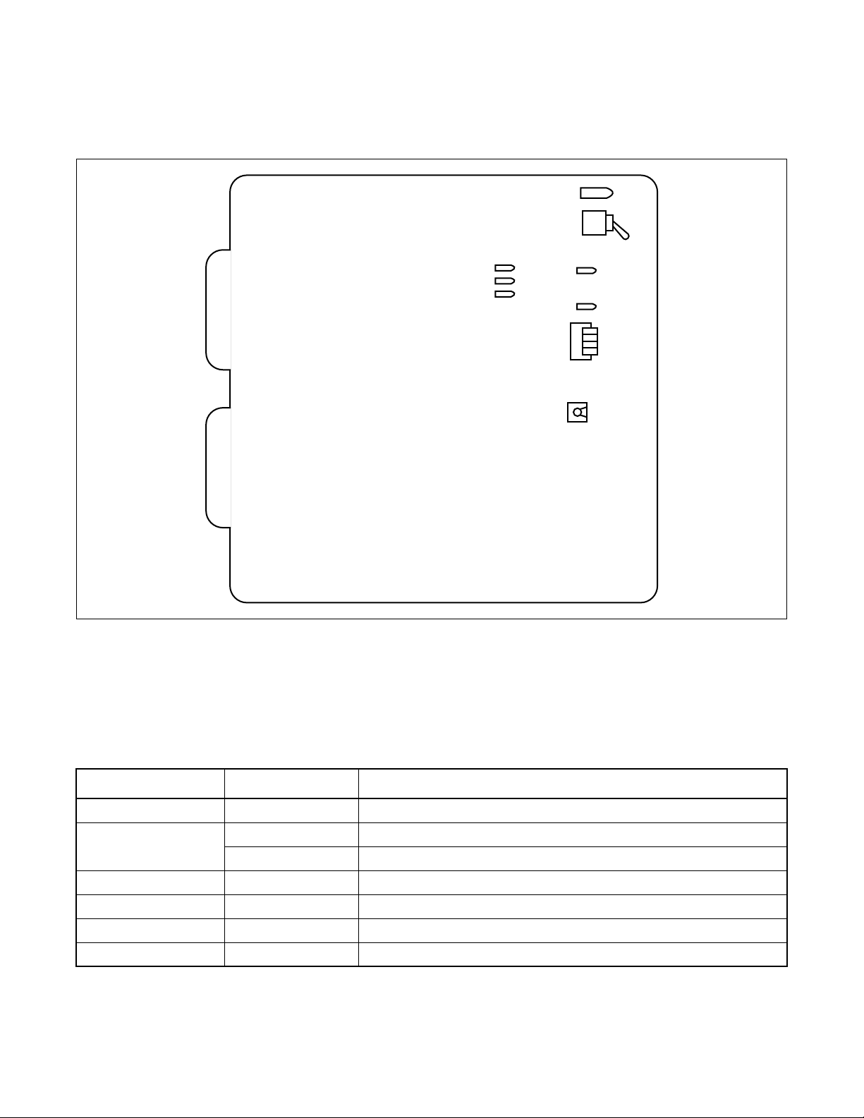
PA-PC94
Data Link Multiplexer
3. Face Layout of Lamps and Switches
The face layout of lamps and switches is shown in Figure 2-15.
OPE
MB KEY
LYR
LB
LOAD
ACT
PWALM
MNT
MODE
Figure 2-15 Face Layout of PA-PC94 (DLMX)
4. Lamp Indications
The contents of lamp indications on this circuit card are shown in the table below:
LAMP NAME COLOR STATE
OPE Green Remains lit while this circuit card is in normal operation.
ACT
LYR OFF Off when this circuit card is in normal operation.
LB OFF Off when this circuit card is in normal operation.
LOAD OFF Off when this circuit card is in normal operation.
PWALM Red Lights when OBP alarm
CHAPTER 2 ND-70182 (E)
Page 44
Revision 4.0
Green Lights when this circuit card is in a active state.
OFF Off when this circuit card is in a stand-by state.

5. Switch Settings
Standard settings of switches on this circuit card are shown in the table below.
PA-PC94
Data Link Multiplexer
SWITCH
NAME
SWITCH
No.
MB
0OFF× Fixed to OFF.
1OFF× Fixed to OFF.
MNT
2OFF× Fixed to OFF.
3
0 × Standard setting. (TSW fixed connection)
MODE
1-7 Not used
6. Switch Setting Sheet
SWITCH
NAME
MB
SWITCH SHAPE REMARKS
SETTING
STANDARD
SETTING
MEANING
UP Circuit card make-busy.
DOWN Circuit card make-busy cancel
ON Make-busy-request.
OFF Cancel the make-busy-request.
ON
MNT
MODE
ON
3
2
1
0
0
ND-70182 (E) CHAPTER 2
Page 45
Revision 4.0

PA-PW54-A
Dual Pow er
PA-PW54-A
Dual Power
1. General Function
The PA-PW54-A (DPWR) c ir cuit ca rd suppli es ope ra ti ng power to circuit cards located in the PIM. The
-48 V input power source, which is converted to +5 V, -5 V, and +12 V, is distributed to each circuit card in
the PIM. This card also has a Ringing Generator Unit (RG U ), whose output frequency and voltage can be
selected from 20 Hz, 25 Hz, 75 Vrms, 90 Vrms by switch setting on this card. In addition, a Howler Tone
circuit resides on this card.
PA-PW55-A (PWR)
HOW
REL
DC-DC
RGU
SUB
PWR
NFB
+5V, +12V, -5V
CR (For LC)
HOW (For LC)
-48 V (For LC, TRK)
+80 V (For MWL)
PA-PW54-A (DPWR)
DC-DC
RGU
HOW
SUB
PWR
NFB
REL
-48 V
Note:
The +80V input is required for activating Message Waiting Lamps (MWLs) .
Figure 2-16 Location of PA-PW54-A (DPWR) Card in the System
CHAPTER 2 ND-70182 (E)
Page 46
Revision 4.0
+80V (Option)
Note

2. Mounting Location/Conditions
This circui t card is mounted in the following slot.
PA-PW54-A
Dual Power
PIM
Mounting Module
PIM
00 01 02 03 04 05 06 07 08 09 10 11 12 13 14 15 16 17 18 19 20 21 22 23
(PA-PW54-A)
DPWR
ND-70182 (E) CHAPTER 2
Page 47
Revision 4.0

PA-PW54-A
Dual Pow er
3. Face Layout of Lamps, Switches, and Connectors
The face layout of lamps, switches, and connec tor s o n this circuit card is shown in Figure 2-17.
SW4
-48V SW
-48V
DC
INPUT
+80VOUT
5A
125V
AC/DC
5.0
A
PAPW54
-A
U
P
( )
-48VSW-48V
CONN
IN
FUSE
FUSE
SIDE VIEW
Figure 2-17 Face Layout of PA-PW54-A (DPWR) Card
MB
0.5
A
RST
RGUOUT
0.5A
125V
AC/DC
HOW ALM
25A
+80V ON
-48V ON
RGU ON
DC ON
OPE
CPU ALM
DC ALM
RGU ALM
-48VOUT
AC250V
DC125V
FRONT VIEW
25A
CHAPTER 2 ND-70182 (E)
Page 48
Revision 4.0

4. Lamp Indications
Lamp indications for this circuit card are shown in the table below.
LAMP NAME COLOR STATE
+80V ON Green Remains lit while +80 V input power is being supplied.
–48 V ON Green R emai ns lit while –48 V input power is being supplied.
RGU ON Green Remains lit whil e RGU output is in progress.
DC ON Green Remains lit while +5 V, +12 V, and –5 V are being output normally.
OPE Green Lights when information exchange with the CPU is possible.
CPUALM Red Lights when reset of the microprocessor has been activated.
DCALM Red Lights when +5 V, +12 V, or –5 V outputs alarm.
RGUALM Red Lights when RGU voltage alarm.
HOWALM Red Lights when howler alarm.
5. Switch Settings
PA-PW54-A
Dual Power
This circuit card has the fo llowing switches.
SWITCH
NAME
–48V SW —
RESET —
MB —
SW4
SWITCH
No.
1
2
6. External Interface
No cable connections are required.
SETTING
ON × –48 V input power is supplied.
OFF –48 V input power is not supplied.
PUSH Hardware reset of the circuit card.
— × Normal setting.
ON Make-busy of the circuit card.
OFF × Normal setting.
ON Frequency of Ringing Signal: 25 [Hz]
OFF × Frequency of Ringing Signal: 20 [Hz]
ON × Voltage of Ringing Signal: 90 [Vrms]
OFF Voltage of Ringing Signal: 75 [Vrms]
STANDARD
SETTING
DESCRIPTION
ND-70182 (E) CHAPTER 2
Page 49
Revision 4.0
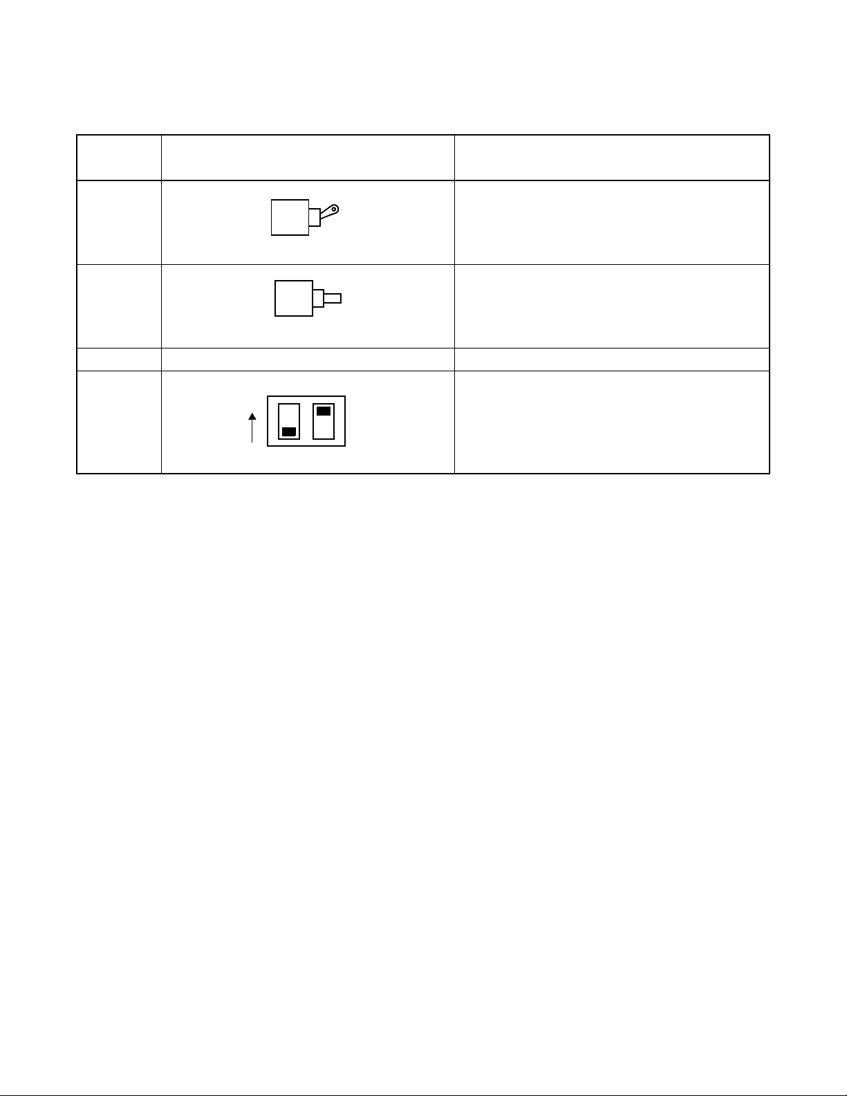
PA-PW54-A
Dual Pow er
7. Switch Setting Sheet
SWITCH
NAME
–48 V
RESET
MB DOWN Circuit card Make-busy cancel
SWITCH SHAPE REMARKS
1
2
ON
SW4
20 [Hz]
90 [Vrms]
CHAPTER 2 ND-70182 (E)
Page 50
Revision 4.0

PA-PW54-B
Dual Power
1. General Function
The PA-PW54-B (DPWR) circuit ca rd supplies operating po wer to ci rcuit cards accommodated in the PIM.
The -48V input power source, which is conver ted to +5V, -5V, and +12V, is distributed to each circui t card
in the PIM. This card is also equipped with a Ringing Generator Unit (RGU), whose output frequenc y and
voltage ca n be sel ected among 20Hz, 25Hz, 75Vrms, 90Vrms by s witch setting on this ca rd. In addition, a
Howler Tone circuit resides on this card.
PA-PW54-B
Dual Power
PA-PW55-B (PWR)
REL
DC-DC
RGU
HOW
SUB
PWR
NFB
+5V, +12V, -5V
CR (For LC)
HOW (For LC)
-48 V (For LC, TRK)
+80 V (For MWL)
PA-PW54-B (DPWR)
DC-DC
RGU
HOW
SUB
PWR
NFB
REL
Note:
-48 V
+80V (Option)
Note
The +80V input is required for activating Message Waiting Lamps (MWLs).
Figure 2-18 Location of PA-PW54-B (DPWR) Card within the System
ND-70182 (E) CHAPTER 2
Page 51
Revision 4.0

PA-PW54-B
Dual Pow er
2. Mounting Location/Conditions
This circui t card is mounted in the following slot.
Mounting Module
00 01 02 03 04 05 06 07 08 09 10 11 12 13 14 15 16 17 18 19 20 21 22 23
(PA-PW54-B)
DPWR
PIM
PIM
CHAPTER 2 ND-70182 (E)
Page 52
Revision 4.0

3. Face Layout of Lamps, Switches, and Connectors
The face layout of lamps, switches, and connec tor s o n this circuit card is shown in Figure 2-19.
-48V
-48VSW-48V
DC
SW4
-48V SW
INPUT
+80VOUT
125V
AC/DC
CONN
5A
5.0
A
PAPW54
- B
U
P
( )
IN
PA-PW54-B
Dual Power
FUSE
FUSE
SIDE VIEW
Figure 2-19 Face Layout of PA-PW54-B (DPWR) Card
MB
0.5
A
RST
RGUOUT
-48VOUT
0.5A
125V
AC250V
AC/DC
DC125V
+80V ON
-48V ON
RGU ON
DC ON
OPE
CPU ALM
DC ALM
RGU ALM
HOW ALM
FRONT VIEW
25A
20A
ND-70182 (E) CHAPTER 2
Page 53
Revision 4.0

PA-PW54-B
Dual Pow er
4. Lamp Indications
The contents of lamp indications on this circuit card are shown in the table below.
LAMP NAME COLOR STATE
+80V ON Green Remains lit while +80 V input power is being supplied.
–48 V ON Green Remains lit while –48 V input power is being supplied.
RGU ON Green Remains lit while RGU output is in progress.
DC ON Green Remains lit while +5 V, +12 V, and –5 V are being output normally .
OPE Green Lights when information exchange with the CPU is possible.
CPUALM Red Lights when reset of the microprocessor has been activated.
DCALM Red Lights in the case of +5 V, +12 V, or –5 V outputs alarm.
RGUALM Red Lights in the case of RGU voltage alarm.
HOWALM Red Lights in the case of howler alarm.
5. Switch Settings
This circuit card has the fo llowing switches.
SWITCH
NAME
–48V SW —
RESET —
MB —
SW4
SWITCH
No.
1
2
6. External Interface
No cable connections are required.
SETTING
ON × –48V input power is supplied.
OFF –48V input power is not supplied.
PUSH Hardware reset of the circuit card.
— × Normal setting
ON Make busy of the circuit card.
OFF × Normal setting
ON Frequenc y of Ringing Signal: 25 [Hz]
OFF × Frequency of Ringing Signal: 20 [Hz]
ON × Voltage of Ri nging Signal: 90 [Vrms]
OFF Voltage of Ringing Signal: 75 [Vrms]
STANDARD
SETTING
DESCRIPTION
CHAPTER 2 ND-70182 (E)
Page 54
Revision 4.0

7. Switch Setting Sheet
PA-PW54-B
Dual Power
SWITCH
NAME
–48 V
RESET
MB DOWN Circuit card make busy cancel
SW4
SWITCH SHAPE REMARKS
20 [Hz]
90 [Vrms]
ON
1
2
ND-70182 (E) CHAPTER 2
Page 55
Revision 4.0

PA-PW55-A
Power
PA-PW55-A
Power
1. General Function
The PA-PW55-A (PWR) circuit card supplies operating po we r to circ uit car ds locat ed in the PIM. The -48
V input power source , which is converted to +5 V, -5 V, and +12 V, is distribut ed to ea ch circuit card in the
associated PIM. This card also has a Ringing Generator Unit (RGU), whose output frequency and voltage
can be selected fro m 20 Hz, 25 Hz, 75 Vrms, 90 Vrms by s witch s etting o n th is card. I n addi tion, a Howler
Tone circuit resides on this card.
PA-PW55-A (PWR)
DC-DC
HOW
REL
RGU
SUB
PWR
NFB
+5V, +12V, -5V
CR (For LC)
HOW (For LC)
-48 V (For LC, TRK)
+80 V (For MWL)
PA-PW54-A (DPWR)
DC-DC
RGU
HOW
SUB
PWR
NFB
REL
-48 V
Note:
The +80V input is r equired for activating Message Waiting Lamps (MWLs) .
Figure 2-20 Location of PA-PW55-A (PWR) Card in the System
CHAPTER 2 ND-70182 (E)
Page 56
Revision 4.0
+80V (Option)
Note

2. Mounting Location/Conditions
This circui t card is mounted in the following slots.
PA-PW55-A
Power
PIM
Mounting Module
PIM
00 01 02 03 04 05 06 07 08 09 10 11 12 13 14 15 16 17 18 19 20 21 22 23
(PA-PW55-A)
PWR
ND-70182 (E) CHAPTER 2
Page 57
Revision 4.0

PA-PW55-A
Power
3. Face Layout of Lamps, Switches, and Connectors
The face layout of lamps, switches, and connec tor s o n this circuit card is shown in Figure 2-21.
SW4
-48V SW
-48V
DC
INPUT
+80VOUT
5A
125V
AC/DC
5.0
A
PAPW55
-A
U
P
( )
-48VSW-48V
CONN
IN
FUSE
FUSE
SIDE VIEW
Figure 2-21 Face Layout of PA-PW55-A Card
MB
0.5
A
RST
RGUOUT
0.5A
125V
AC/DC
HOW ALM
25A
+80V ON
-48V ON
RGU ON
DC ON
OPE
CPU ALM
DC ALM
RGU ALM
-48VOUT
AC250V
DC125V
FRONT VIEW
25A
CHAPTER 2 ND-70182 (E)
Page 58
Revision 4.0

4. Lamp Indications
Lamp indications for this circuit card are shown in the table below.
LAMP NAME COLOR STATE
+80V ON Green Remains lit while +80 V input power is being supplied.
–48 V ON Green R emai ns lit while –48 V input power is being supplied.
RGU ON Green Remains lit whil e RGU output is in progress.
DC ON Green Remains lit while +5 V, +12 V, and –5 V are being output normally.
OPE Green Lights when information exchange with the CPU is possible.
CPUALM Red Lights when reset of the microprocessor has been activated.
DCALM Red Lights when +5 V, +12 V, or –5 V outputs alarm.
RGUALM Red Lights when RGU voltage alarm.
HOWALM Red Lights when howler alarm.
5. Switch Settings
PA-PW55-A
Power
This circuit card has the fo llowing switches.
SWITCH
NAME
–48 V SW
RESET
MB —
SW4
SWITCH
No.
1
2
6. External Interface
No cable connections are required.
SETTING
ON × –48 V input power is supplied.
OFF –48 V input power is not suppli e d.
PUSH Hardware reset of the circuit card.
— × Normal setting
ON Make-busy of the circuit card.
OFF × Normal setting
ON Frequency of Ringing Signal: 25 [Hz]
OFF × Frequency of Ringing Signal: 20 [Hz]
ON × Voltage of Ringing Signal: 90 [Vrms]
OFF Voltage of Ringing Signal: 75 [Vrms]
STANDARD
SETTING
DESCRIPTION
ND-70182 (E) CHAPTER 2
Page 59
Revision 4.0
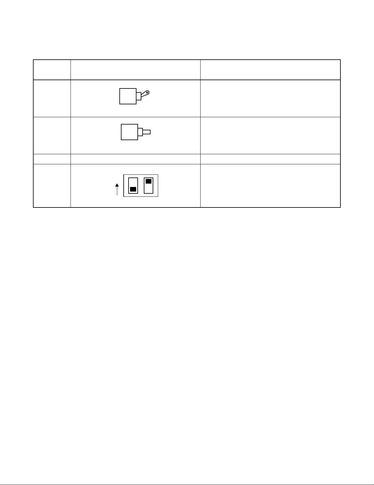
PA-PW55-A
Power
7. Switch Setting Sheet
SWITCH
NAME
–48 V
RESET
MB DOWN Circuit card Make-busy cancel.
SWITCH SHAPE REMARKS
12
ON
SW4
20 [Hz]
90 [Vrms]
CHAPTER 2 ND-70182 (E)
Page 60
Revision 4.0

PA-PW55-B
Power
1. General Function
The PA-PW55-B (PWR) circuit card supplies operating power to circuit cards accommodated in the PIM.
The -48V input power source, which is conver ted to +5V, -5V, and +12V, is distributed to each circui t card
in the associat ed PIM. This card is al so equipped with a Ri nging Generator U nit (RGU), whose out put
frequency and voltage can be selected among 20Hz, 25 Hz, 75Vrms, 90Vrms by swi tch set ting on thi s card.
In addition, a Howler Tone circuit resides on this card.
PA-PW55-B
Power
PA-PW55-B (PWR)
REL
DC-DC
RGU
HOW
SUB
PWR
NFB
+5V, +12V, -5V
CR (For LC)
HOW (For LC)
-48 V (For LC, TRK)
+80 V (For MWL)
PA-PW54-B (DPWR)
DC-DC
RGU
HOW
SUB
PWR
NFB
REL
Note:
-48 V
+80V (Option)
Note
The +80V input is r equi red for activating Message Waiting Lamps (MWLs).
Figure 2-22 Location of PA-PW55-B (PWR) Card Within the System
ND-70182 (E) CHAPTER 2
Page 61
Revision 4.0

PA-PW55-B
Power
2. Mounting Location/Conditions
This circui t card is mounted in the following slots.
Mounting Module
00 01 02 03 04 05 06 07 08 09 10 11 12 13 14 15 16 17 18 19 20 21 22 23
(PA-PW55-B)
PWR
PIM
PIM
CHAPTER 2 ND-70182 (E)
Page 62
Revision 4.0

3. Face Layout of Lamps, Switches, and Connectors
The face layout of lamps, switches, and connec tor s o n this circuit card is shown in Figure 2-23.
-48V
-48VSW-48V
DC
SW4
-48V SW
INPUT
+80VOUT
125V
AC/DC
CONN
5A
5.0
A
PAPW55
-B
U
P
( )
IN
PA-PW55-B
Power
FUSE
FUSE
SIDE VIEW
Figure 2-23 Face Layout of PA-PW55-B Card
MB
0.5
A
RST
RGUOUT
-48VOUT
0.5A
125V
AC250V
AC/DC
DC125V
+80V ON
-48V ON
RGU ON
DC ON
OPE
CPU ALM
DC ALM
RGU ALM
HOW ALM
FRONT VIEW
25A
20A
ND-70182 (E) CHAPTER 2
Page 63
Revision 4.0

PA-PW55-B
Power
4. Lamp Indications
The contents of lamp indications on this circuit card are shown in the table below.
LAMP NAME COLOR STATE
+80V ON Green Remains lit while +80 V input power is being supplied.
–48 V ON Green Remains lit while –48 V input power is being supplied.
RGU ON Green Remains lit while RGU output is in progress.
DC ON Green Remains lit while +5 V, +12 V, and –5 V are being output normally .
OPE Green Lights when information exchange with the CPU is possible.
CPUALM Red Lights when reset of the microprocessor has been activated.
DCALM Red Lights in the case of +5 V, +12 V, or –5 V outputs alarm.
RGUALM Red Lights in the case of RGU voltage alarm.
HOWALM Red Lights in the case of howler alarm.
5. Switch Settings
This circuit card has the fo llowing switches.
SWITCH
NAME
–48V SW
RESET
MB —
SW4
SWITCH
No.
1
2
6. External Interface
No cable connections are required.
SETTING
ON
OFF –48V input power is not supplied.
PUSH Hardware reset of the circuit card.
—
ON Make busy of the circuit card.
OFF
ON Frequenc y of Ringing Signal: 25 [Hz]
OFF
ON
OFF Voltage of Ringing Signal: 75 [Vrms]
STANDARD
SETTING
×
×
×
×
×
DESCRIPTION
–48V input power is supplied.
Normal setting
Normal setting
Frequency of Ringi ng Sign al : 20 [Hz]
Voltage of Ringing Signal: 90 [Vrms]
CHAPTER 2 ND-70182 (E)
Page 64
Revision 4.0
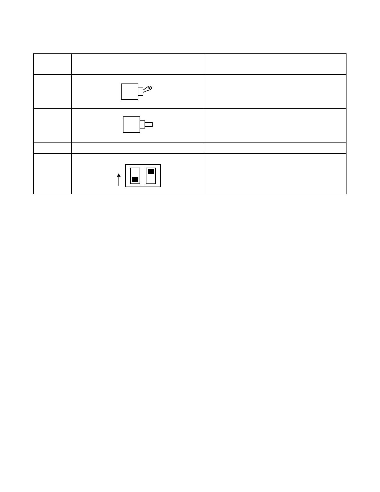
7. Switch Setting Sheet
PA-PW55-B
Power
SWITCH
NAME
–48 V
RESET
MB DOWN Circuit card make busy cancel
SW4
SWITCH SHAPE REMARKS
12
ON
20 [Hz]
90 [Vrms]
ND-70182 (E) CHAPTER 2
Page 65
Revision 4.0

PH-IO24
Input/Output Controller
PH-IO24
Input/Output Controller
1. General Function
The PH-IO24 (IOC) circuit card supplies the system with a serial interface, which conforms to RS-232C,
between external equipment such as the Maintenance Administration Terminal (MAT), Station Message
Detail Recording System (SMDR), Message Center Interface (MCI). Property Management System
(PMS). The relationship between the IOC card and the associated cards is as follows, when the CPU is
composed in a dual configuration.
Note:
Firmware SP-3290 IO24 LV2 PROG-A is required in the Hotel system for PMS and Ho tel Printer.
FDD/HDD #0
CPU
BOARD
#0
I/O
GT #1
Business
MAT
SMDR
MCI
MISC/IOC
IOC
for
MISC
EMA
Hotel Printer
GT #0
IOC
for
Hotel
PMS
MISC I/O BUS
CPU
BOARD
#1
I/O
FDD/HDD #1
Figure 2-24 Location of PH-IO24 (IOC) Card within the System
CHAPTER 2 ND-70182 (E)
Page 66
Revision 4.0

2. Mounting Location/Condition
The IOC cards can be accommodated in the shaded slots (02, 03) as shown below.
PH-IO24
Input/Output Controller
Note:
When using Business system and Hotel system, prepare the circuit card for each system.
Mounting Module
00 01 02 03 04
IOC #1
IOC #0
LPM
3. Face Layout of Lamps, Switches and Connectors
The face layout of lamps, switches and connectors on this circuit ca rd is shown in Figure 2-25.
OPE
MB
MBR
IOC ALM
PORT0
PORT1
PORT2
SW50
PORT3
Figure 2-25 Face Layout of PH-IO24 (IOC) Card
ND-70182 (E) CHAPTER 2
Page 67
Revision 4.0

PH-IO24
Input/Output Controller
4. Lamp Indications
The table below shows lamp indications on this circuit card.
LAMP NAME COLOR DESCRIPTION
OPE/MB Green This circuit card is operating normally .
Red This circuit card is placed in the make busy state.
IOC ALM Red Clock down WDT alarm occurs to the microprocessor.
POR T 0 - PORT3 RS-232C signal status indi cati on . n = port number (0-3)
SDn Green SD:Send Data
RDn Green RD:Receive Data
ERn Green ER:Equipment Ready
DRn Green DR:Data Ready
CDn Green CD:Carrier Detect
5. Switch Settings
The following is a brief description of the switches on this circuit card. When a switch has a standard set-
ting, it is indicated with “×” in the table below.
SWITCH
NAME
MB
MBR
SW50
SWITCH
NO.
SETTING
UP The circuit card is placed into a make busy status.
DOWN
UP The circuit card is placed into a make busy request status.
DOWN
ON This circuit card is used as the extended I/O circuit card #1.
1
OFF This circuit card is used as the extended I/O circuit card #0.
ON
2
OFF
ON Free Wheeling with ACK signal (For Hotel System Only).
2
OFF
STANDARD
SETTING
×
×
×
×
DESCRIPTION
Cancellation of Make Busy.
Cancellation of Make Busy Request.
Not used (For Busi nes s Sy stem O nl y).
Free Wheeling.
3
4
CHAPTER 2 ND-70182 (E)
Page 68
Revision 4.0
ON
OFF
ON
OFF
×
Not used
Not used
×

Input/Output Controller
6. External Interface
As illustrated below , the “68PH S 2PORTS CA-A” cable is required to connect e xternal equipment such as
the MAT, SMDR, MCI and PRT.
Securely insert the connector of the 68PH S 2PORTS CA-A into the appropriate MISC connector. Refer to the table listed below.
RS-232C cable (Note 2)
MISC 3B/4B (Note 1)
Backplane
PH-IO24
(IOC)
AMP AMP
68PH S 2PORTS CA-A
Circuit #0
Circuit #1
TYP0 TYP1
To RS-232C
Terminal
PH-IO24
Note 1:
The relationship between the MISC connectors and the mounting
slot of the IOC (PH-IO24) circuit card is shown below.
Mounting Slot
02
03
Note 2:
The type of cables varies depending on a connected terminal and/or
whether modems are used or not. More detailed information on the
connecting cables is explained in the “Installation Procedure
Manual”.
68PH S 2PORTS CA-A
Circuit #2
MISC 3A/4A (Note 1)
Circuit #3
Pin Signal name
01 SD
IOC Circuit Number
#0, #1
#2, #3
#0, #1
#2, #3
MISC Connector
MISC 3B
MISC 3A
MISC 4B
MISC 4A
02 RD
03 RS
04 CS
05
06
07
08
09
10
11
12
13
14
15
16
17
TYP0, 1 Lead Accommodation
Figure 2-26 External Cable Connection for PH-IO24 (IOC)
TYP1TYP0
TYP0, 1 Connector
DR
SG
CD
ER
PB/CI
RT
ST1
ST2
Pin Signal name
26
27
28
29
30
31
32
33
34
35
36
37
38
39
40
41
42
ND-70182 (E) CHAPTER 2
Page 69
Revision 4.0

PH-IO24
Input/Output Controller
7. Switch Setting Sheet
SWITCH
NAME
MB
MBR
SW50
SWITCH SHAPE REMARKS
ON
1
2 3 4
Meaning of SW50-1:
ON:
OFF:
This card is used as the No. 1 circuit card.
This card is used as the No. 0 circuit card.
CHAPTER 2 ND-70182 (E)
Page 70
Revision 4.0

PH-M22
MMC
1. General Function
The main functions of the PH-M22 circuit card are:
• To coll ect t he key settin g inform at ion on the TOPU of the ISW a nd se nd the infor ma tion to the IS W/
the other LNs, depending on the ISEL key setting on the ISW.
• To collect various alarm information from all the IMGs/ISW and activate MJ/MN LED on the TOPU
display.
This circuit card is used for the IMX-U system.
PH-M22
MMC
LN
ISW
PH-M22
RECEIVER
RELAY
PZ-DK227
(TOP KEY)
ISEL
SEL
AUDIBLE
AND
VISUAL
ALARM
INDICATING
PANEL
PH-PC40
EMA
PZ-DK222
(TOP KEY)
PH-M22
PH-PC40
RECEIVER
EMA
RELAY
LN
PZ-DK222
(TOP KEY)
PH-M22
PH-PC40
RECEIVER
EMA
KEY INFORMATION
ALM INFORMATION
Figure 2-27 Location of PH-M22 (MMC)
RELAY
ND-70182 (E) CHAPTER 2
Page 71
Revision 4.0

PH-M22
MMC
2. Mounting Location/Condition
This circuit card can be mounted in the shaded slots shown below.
Mounting Module
00 01 02 03 04
MMC
LPM
CPRAQ-A/CPRAS-A
CPRAQ-A/CPRAS-A
3. Face Layout of Lamps, Switches, and Connectors
The face layout of lamps, switches, and connectors are shown in Figure 2-28.
OPE
MB
Figure 2-28 Face Layout of PH-M22 (MMC)
CHAPTER 2 ND-70182 (E)
Page 72
Revision 4.0
CN7
CN6
CN5
CN4
CN3
CN2
CN1
CN0
KEY

4. Lamp Indications
The contents of lamp indications on this circuit card are shown in the table below.
LAMP NAME COLOR STATE
OPE Green Lights when this circuit card is in operation.
5. Switch Settings
Switch settings on this circuit card are shown in the table below.
PH-M22
MMC
SWITCH
NAME
MB
SETTING
UP Circuit Card make-busy
DOWN × Circuit Card make-busy cancel
STANDARD
SETTING
MEANING
ND-70182 (E) CHAPTER 2
Page 73
Revision 4.0

PH-M22
MMC
6. External Interface
LPM
MISC0A
Connector
MMC (PH-M22) : Slot No.00
68PH EXMISC CA
AUDIBLE AND VISU AL
ALARM INDICATING PANEL
MDF
MJ
MN
REAR VIEW
68PH EXMISC CA
1
2
MPALM
3
4
EXTAA
5
6
BELAA
7
-
8
MNAA
9
SUPAA
10
MJAA
11
12
(BASEU)
(RPT0)
26
27
28
29
30
31
32
33
34
35
36
37
-48V
MNBA
SUPBA
MJBA
RPT Terminal on front
of the BASEU
01 02 03 04 0501 02 03 04 05
G
(RPT1)
BELAA
MNAA
SUPAA
MJAA
MNBA
SUPBA
MJBA
RPT1(G)
RPT0(-48V)
BELL
68PH EXMISC CA and
Installation Cable
MDF
MJ/MN/BELL
Figure 2-29 Connection of Alarm Indicating Panel
CHAPTER 2 ND-70182 (E)
Page 74
Revision 4.0

7. Switch Setting Sheet
SWITCH NAME SWITCH SHAPE REMARKS
PH-M22
MMC
MB Note: Normal operating mode is down.
ON
ND-70182 (E) CHAPTER 2
Page 75
Revision 4.0

PH-M16/PH-M23
Line Test
PH-M16/PH-M23
Line Test
1. General Function
This circuit card controlled by CPU is used for line test of a subscriber’s line. Th e circuit card su pports to
send Howler Tone to ex t ernal test equipmen t, besides the circuit car d can detect or send various tones, and
send PB (DTMF) signal for automatic trunk test.
Note:
A system cannot send Howler Tone during line test. The number of available lines within the line test/automatic trunk test at the sam e time is only one.
TEL
TEL
PIM
LPRA
TEST
EQ
LTST
EXTENDED I/O BUS
LC
LC
EXTENDED I/O BUS
I
N
T
GT
EXGT
TSW
CPU
Figure 2-30 Location of PH-M16/PH-M23 (LTST) Card Within the System
CHAPTER 2 ND-70182 (E)
Page 76
Revision 4.0

2. Mounting Location/Condition
The LTST circuit card can be accommodated in the shaded slots (00, 01, 02) as shown below:
PH-M16/PH-M23
Line Test
Note:
IMX: Slot 00, Slot 01, Slot 02.
IMX-U: Slot 01, Slot 02 (Considering PH-M22 MMC)
Mounting Module
00 01 02 03 04
PH-M16/PH-M23
PH-M16/PH-M23
PH-M16/PH-M23
LPM
3. Face Layout of Lamps, Switches, and Connectors
The face layout of lamps, switches, and connec tor s o n this circuit card is shown in Figure 2-31.
Note:
OPE/MB
MB
SW0
CRIN
Figure 2-31 Face Layout of PH-M16/PH-M23 (LTST) Card
CRIN is used to connect with CRIN test equipment.
ND-70182 (E) CHAPTER 2
Page 77
Revision 4.0

PH-M16/PH-M23
Line Test
4. Lamp Indications
LAMP NAME COLOR DESCRIPTION
OPE/MB
5. Switch Settings
SWITCH
NAME
MB
SW0
SWITCH
NO
Green This circuit card is operating in normal mode.
Red This circuit card is Make-b usy.
SETTING
STANDARD
SETTING
UP Circuit card Make-busy
DOWN Circuit card Make-busy cancel
1ON ×
2
ON ×
Setting of a condition of DT detecti on
(440Hz+350Hz)
Setting of a condition of RBT detection
(440Hz+480Hz)
ON Time of PB (DTMF) signal sending (67msec.)
3
OFF × Time of PB (DTMF) signal sending (133msec.)
Setting of M-wire control which is concerned with
ON
sending test tone of ODT
(Set soft control or E-wire loop-back)
4
Setting of M-wire control which is concerned with
OFF
sending test tone of ODT
(Set soft control only)
MEANING
5
6
7
8
CHAPTER 2 ND-70182 (E)
Page 78
Revision 4.0
BASIC INTERVAL TIMER
SW0
5678TIME
ON OFF OFF OFF 8
ON ON OFF OFF 16
ON ON ON OFF 32
ON ON ON ON 64
µ
µ
µ
µ
6. External Interface
MISC Connector Accommodation
Circuit Card Backboard Connector
Connector Name
PH-M16/PH-M23
Line Test
Slot Number
LPM Backboard
LPM
MISC
00 01 02 03 04
PH-M16/PH-M23
PH-M16/PH-M23
PH-M16/PH-M23
Circuit Card Backboard Conn ec tor
68PH EXMISC CABLE
26
27
28
29
30
31
32
33
34
35
36
37
38
39
40
41
42
43
44
45
46
47
48
49
50
MISC CONNECTOR
TE
TELB
LCB
THOWB
THOWS
SE TCR
INB
1
2
3
4
5
6
7
8
9
10
11
12
13
14
15
16
17
18
19
20
21
22
23
24
25
TM
TELA
LCA
THOWA
ONHK
ATM
ATAATB
OUTAOUTB
TA1TB1
INA
MISC CONNECTOR
Figure 2-32 LT Connector Lead Accommodation
ND-70182 (E) CHAPTER 2
Page 79
Revision 4.0
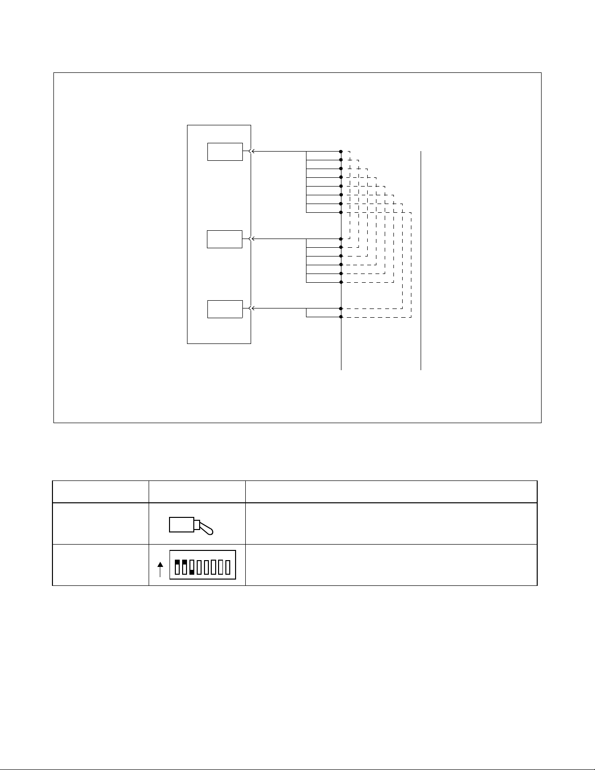
PH-M16/PH-M23
Line Test
PBX
LTST
TLT
LC
MDP
TM
TE
OUTA
OUTA
INA
INB
TA1
TB1
E
M
RA
RB
TA
TB
A
B
Figure 2-32 Connecting Route Diagram
7. Switch Setting Sheet
SWITCH NAME SWITCH SHA PE REMARKS
4
5
ON (MB)
OFF
678
MB
1ON2 3
SW0
CHAPTER 2 ND-70182 (E)
Page 80
Revision 4.0

PH-PC36
Multiplexer
1. General Function
The PH-PC36 (MUX) circuit card is an interface card for mounting line cir cui ts and/or trunks. In between
the CPR and the Port Microprocessor (PM) of the line/trunk circuit, this circuit card provides an interface
for PM control and management by the CPU. Lik ewi se in between the TSW and th e line circuit /trunks, this
circuit card pro vides an inter face for mult iplexi ng/de-multi plexing of voice Pu lse Code Modulat ion (PCM)
information and digital data information.
PH-PC36
Multiplexer
LC/TRK
PM
LC/TRK
PM
LC/TRK
PM
LC/TRK
PM
CPR
GT
TSW/INT/PLO
MUX
MUX
PCM HW
PM BUS
MUX
PCM HW
PM BUS
MUX
PCM HW
PM BUS
PCM HW
PM BUS
Figure 2-33 Location of PH-PC36 (MUX) Card in the 1 IMG System
ND-70182 (E) CHAPTER 2
Page 81
Revision 4.0

PH-PC36
Multiplexer
CPR 1
ISAGT
CPR 0
ISAGT
GT 0
DLKC 1
DLKC 0
GT 1
TDSW
13
TDSW
03
TDSW
12
TDSW
02
TDSW
11
TDSW
01
TDSW
10
TDSW
00
MUX
MUX
MUX
MUX
MUX
MUX
MUX
MUX
MUX
MUX
MUX
MUX
MUX
MUX
MUX
MUX
PCM HW
PM BUS
PCM HW
PM BUS
PCM HW
PM BUS
PCM HW
PM BUS
PCM HW
PM BUS
PCM HW
PM BUS
PCM HW
PM BUS
PCM HW
PM BUS
PCM HW
PM BUS
PCM HW
PM BUS
PCM HW
PM BUS
PCM HW
PM BUS
PCM HW
PM BUS
PCM HW
PM BUS
PCM HW
PM BUS
PCM HW
PM BUS
Line/Trunk PM
Line/Trunk PM
IMG 3
Line/Trunk PM
Line/Trunk PM
Line/Trunk PM
Line/Trunk PM
IMG 2
Line/Trunk PM
Line/Trunk PM
Line/Trunk PM
Line/Trunk PM
IMG 1
Line/Trunk PM
Line/Trunk PM
Line/Trunk PM
Line/Trunk PM
IMG 0
Line/Trunk PM
Line/Trunk PM
Figure 2-34 Location of PH-PC36 (MUX) Card in the 4 IMG System
CHAPTER 2 ND-70182 (E)
Page 82
Revision 4.0

PH-PC36
Multiplexer
LN
LC/TRK
LC/TRK
LC/TRK
LC/TRK
LC/TRK
LC/TRK
LC/TRK
LC/TRK
DLKC0
PLO 0
MUX00
MUX01
MUX02
MUX03
TSW00
MUX
TSW01
TSW02
TSW03
TSW10
TSW11
TSW12
TSW13
MUX
MUX10
MUX11
MUX12
MUX13
LC/TRK
LC/TRK
LC/TRK
LC/TRK
DLKC1
PLO 1
LC/TRK
LC/TRK
LC/TRK
LC/TRK
ISW
HSW00
PLO 0
TSW00
TSW01
TSW02
TSW03
HSW01
HSW10
HSW11
TSW10
TSW11
TSW12
TSW13
Figure 2-35 Location of PH-PC36 (MUX) Card in the IMX-U System
ND-70182 (E) CHAPTER 2
PLO 1
Page 83
Revision 4.0

PH-PC36
Multiplexer
The PCM highway running is illustrated in the figure below. There are sixteen 2Mbps PCM highways
(HW0 - HW15) in the PIM. Each PCM highw ay runs from a card slot to the MUX ci rcuit card. For inst ance,
highway number zero (HW0) appears in Slot 04 and also Slot 05, thus the HW0 carries the PCM of the
Group 0, 1, 2 and 3.
Likewise, the HW6, 7, 14, 15 cover the Groups 24 through 31. However, the time slots of Groups 24 and
25 are exclusively used for the Speech Path Memory (SPM).
All highways in the PIM lea d to a MUX card, so 512 ti me s lot s (32 time slots per highw ay × 16 highw ays
= 512 time slots) of PCM are multiplexed/de-multiplexed at a MUX and sent/received to/from the TSW
circuit card across the 32.786Mbps of the Low Voltage Differential Signaling (LVDS).
Also the MUX card pro vides the PM bus in terf ace. The CPR con trols and a dministra tes the PM of th e line/
trunk circuit card via the TSW and the MUX.
In addition, this circuit card supports 3-P arty Conference (CFT) function and is equipped with eight circuit s
of 3-Party Conference. The CFT appear in time Slots 8 through 3 1 of the HW13 (Group 21 - 23).
Slot number of the PIM U-A
Group (G) number of the LENS
00 01 02 03 04 05 06 07 08 09 10 11
PWR
(24)
Group 24 and 25 are used
for the SPM
HW6
PWR
01
23
45
HW0 HW1 HW2
(25)
2627
2829
HW7
31 30
1011
89
12131415
HW4
HW3
67
16171819
8 circuits of CFTs
13 14 15 16 17 18 19 20 21 22 23
12
MUX#1
MUX#0
89
3031
11
10
HW11
20212223
HW5
5
3
67
2
4
4
HW9 HW10
2829
HW15
01
HW8
2627
HW1
2Mbps (32 time slots) of PCM highway
1415
13
12
19
18
1617
HW12
23
22
21
20
HW13
Figure 2-36 PCM Highway Running
CHAPTER 2 ND-70182 (E)
Page 84
Revision 4.0

2. Mounting Location/Condition
For the 1 IMG system, the PH-PC36 (MUX) card is mount ed in the PIM 1, 2, and 3.
For the 4 IMG system, the PH-PC36 (M UX) card is required in all PIMs.
PH-PC36
Multiplexer
Mounting Module
PIM
00 01 02 03 04 05 06 07 08 09 10 11 12 13 14 15 16 17 18 19 20 21 22 23
PIM
3. Face Layout of Lamps, Switches, and Connectors
The face layout of lamps, switches, and connector s is shown in Figure 2-37.
MUX #0
MUX #1
MUXACT
SYNC
RCLK ALM
PMCLK ALM
OFFON
1
2
3
4
SW01
CFT OPE
Figure 2-37 Face Layout of PH-PC36 (MUX)
ND-70182 (E) CHAPTER 2
MB
MUX
Page 85
Revision 4.0
 Loading...