


查询XPC850供应商
Networking Communication Microprocessors
XPC850 (Rev 0.3)
XPC860
Reliability Report
for
XPC860T
0.42m Single Poly Wafer Fabrication Process
Revision: 5/99

1.0 Purpose and Description
This report summarizes the reliability data for Motorola communication
microprocessors fabricated on the 0.42m single polysilicon process in our wafer
fabrication facility, Mos 11, in Austin, Texas. The current devices fabricated using this
process are given in the table below.
Device Mask Set Design
Revision
XPC850 F98S 0.3 309 x 335 0.42m
XPC860 J24A
H96G
XPC860T J21M 0.2 338 x 347 0.42m
Table 1. Device properties.
All of these devices are currently in their XC phase of product life, which is the
time when design errata are discovered and corrected. Although the 850 and 860 are still
classified as XC devices, they are built using production equipment and processes, and
have completed their reliability qualifications. There are some functional errata on these
devices, which may impact some customers. These errata are expected to be corrected in
revision D of the 860, which we expect to grant MC status to. For a list of current design
errata on these devices, please contact your local Motorola sales person. To locate the
nearest sales office, you can find them on our website at http://mot-sps.com/sales/
sales_web.html
2.0 Assembly / Package Information
B.1
C
Die Size
(mils)
338 x 329
338 x 329
Process
Geometry
0.42m
The XPC850 is assembled in a 256 leaded plastic ball grid array. The XPC860 is
assembled in a 357 lead plastic ball grid array (PBGA). Both packages have been shown
to meet level 3 moisture sensitivity as classified by JEDEC A113. Our volume
production is manufactured in MotorolaÕs Kuala Lumpur, Malaysia facility, however we
have also qualified Citizen Watch Co, in Japan as an alternate assembly site.
2

3.0 Family Qualification Strategy
Motorola uses a ÒfamilyÓ qualification strategy which allows sharing of certain
reliability data across a common design rule / fabrication geometries and packaging types.
Reliability data from other Motorola devices which are designed using the same design
rules and wafer fabrication processes are included with this report.
All of the devices in this report have been in production manufacturing for at least 3
years. The data presented in this report is both data from current production material
and historical data used to qualify devices, processes, and wafer fab and assembly sites.
This report will be updated periodically (typically twice/year) with new reliability data
from subsequent qualifications and reliability monitors.
3
4.0 Qualification Data
Motorola .42m Process Qualification Summary
The following data shows results of our .42m qualifications:
Life Test (+125°C, 4.5V)
Device/Mask Set SS 168 Hrs. 504 Hrs. 1008 Hrs. 2016 Hrs. Failure Details
XPC850 (F98S) rev 0.3 77 1/77 0/76 0/71 --- 168 Hr : Speed degradation failure
1008 Hr: 4 parts missing balls, 1 part
damaged -discounted
XPC850 (F98S) rev 0.3 77 0/77 0/75 0/74 --- 504 /1008 Hr: Damaged part -
discounted
XPC850 (F98S) rev 0.3 77 0/77 0/77 0/72 --- 1008 Hr: Units discounted
XPC850 (F98S) rev 0.3 77 0/77 0/75 0/69 --- 168/504 Hr: Units discounted
XPC860 (J23A) rev A.3 77 0/77 0/77 0/77 0/77 --XPC860 (J23A) rev A.3 77 0/77 0/77 0/77 0/77 ---
XPC860 (J23A) rev A.3 77 0/77 0/77 0/77 0/77 --XPC860 (H96G) rev C.1 77 0/77 0/77 0/77 --XPC860 (H96G) rev C.1 77 0/77 1/77 0/77 --- Functional Failure Ð destroyed in FA
XPC860 (H96G) rev C.1 77 0/77 0/77 0/77 ---
XPC860T (J21M) 77 1/77 0/76 0/75 --- 168 hr: Funct fail, 1008 hr: 1 unit
damaged at test-discounted
68LC060 (G59Y) 77 0/76 0/76 0/63 --- 168/1008 Hr: Parts discounted
68LC060 (G59Y) 77 0/77 0/77 0/77 --- --68LC060 (G59Y) 77 0/77 0/77 0/77 --- --68LC060 (G59Y) 77 0/77 0/77 --- --- --68LC060 (G59Y) 77 1/77 0/76 --- --- 168 Hr: 1 functional fail
Total 1232 3/1231 1/1224 0/1040 0/231 ---
Table 1. Life Test Data.
4
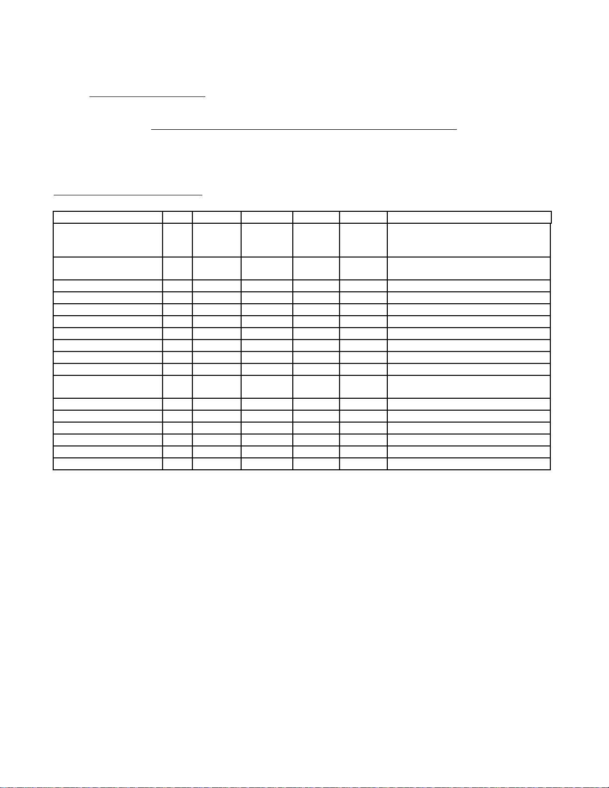
MM
MM
1000.00
100.00
10.00
1.00
Fit Rate (Failures/1E9 Device Hours)
0.10
0 2 0 40 60 80 100 120
FITs vs Junction Temperature: .42u FIT/MTBF Data
Thermal and Voltage Acceleration
eA = 0.5 eV, Beta = 2.5, 90% Confidence
Tj 3 V 3.3 V 3.5 V
40 °C247
60 °C 6 13 22
80 °C 173659
Junction Temperature (°C)
3 V
3.3 V
3.5 V
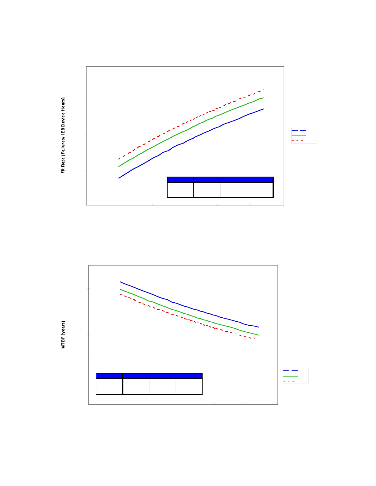
1.00E+06
1.00E+05
1.00E+04
1.00E+03
MTBF (years)
1.00E+02
1.00E+01
1.00E+00
0 20 40 60 80 100 120
MTBF vs Junction Temperature: .42u FIT/MTBF Data
mm
mm
Tj 3 V 3.3 V 3.5 V
40 °C 5.4E+4 2.6E+4 1.6E+4
60 °C 1.8E+4 8.4E+3 5.1E+3
80 °C 6.6E+3 3.1E+3 1.9E+3
eA = 0.5 eV, Beta = 2.5, 90% Confidence
Junction Temperature (°C)
Thermal and Voltage Acceleration
3 V
3.3 V
3.5 V
5
Temp Cycle (-65°C / +150°C)
Die Rev/Mask Set SS PC-MSL3 100 Cyc 500 Cyc 1000 Cyc Failure Details
XPC860 77 0/77 0/77 0/77 1/77 1000 Cyc: 1 fail
XPC860 77 0/77 0/77 0/77 0/77 ---
XPC860 (J23A) rev A.3 77 0/77 0/77 0/77 *0/76 1000 Cyc: missing ball-
discounted
XPC860 (J23A) rev A.3 77 0/77 0/77 0/77 0/77 --XPC860 (J23A) rev A.3 77 0/77 0/77 0/77 0/77 --XPC860 (J23A) rev A.3 77 0/77 0/77 0/77 0/77 --XPC860 (J23A) rev A.3 77 0/77 0/77 0/77 0/77 --XPC860 (J23A) rev A.3 77 0/77 0/77 0/77 0/77 --XPC860 (J23A) rev A.3 77 0/77 0/77 0/77 0/77 ---
Total 693 0/693 0/693 0/693 1/693 ---
Table 2. Temperature Cycle Data (MSL3).
Autoclave (+121°C / 15PSIG)
Die Rev/Mask Set S S PC-MSL3 48 Hrs 96 Hrs 144 Hrs Failure Details
XPC860 77 0/77 0/77 0/77 0/77 ---
XPC860 77 0/77 0/77 0/77 0/77 --XPC860 (J23A) rev A.3 77 0/77 0/77 0/77 0/77 --XPC860 (J23A) rev A.3 77 0/77 --- --- --- Terminated-die
attach problem
XPC860 (J23A) rev A.3 77 0/77 0/77 0/77 0/77 --XPC860 (J23A) rev A.3 77 0/77 0/77 0/77 0/77 --XPC860 (J23A) rev A.3 77 0/77 0/77 0/76 0/76 48 hr:
Mishandled-
discounted
XPC860 (J23A) rev A.3 77 0/77 2/77 8/75 1/67 48 Hr: 2 functional
96 Hr: 8 functional
144 Hr: 1
functional
XPC860 (J23A) rev A.3 60 0/60 0/60 0/60 0/60
XPC860 (J23A) rev A.3 36 0/36 0/36 0/36 0/36
XPC860 (J23A) rev A.3 76 0/76 0/76 0/76 0/76
XPC860 (J23A) rev A.3 77 0/77 0/77 0/77 0/77
XPC860 (J23A) rev A.3 77 1/77 0/76 0/76 0/76 MSL3: functional
Total 942 1/942 2/864 8/861 1/853 ---
Table 3. Autoclave Data (MSL3).
6

THB (+85°C / 85%RH)
Die Rev/Mask Set SS PC-MSL3 168 Hrs 504 Hrs 1008 Hrs Failure Details
XPC860 (J23A)
rev A.3
XPC860 (J23A)
rev A.3
XPC860 (J23A)
rev A.3
XPC860 (J23A)
rev A.3
Total 308 0/307 0/230 0/230 0/229 ---
77 0/77 0/77 0/77 0/76 1008 Hr: Unit discounted
77 0/77 --- --- --- Terminated - die attach problem
77 0/76 0/76 0/76 0/76 PC: Substrate damage-
discounted
77 0/77 0/77 0/77 0/77 ---
Table 4. THB Data (MSL3).
7

Electrostatic Discharge Data
The following ESD data is device specific:
860 ESD Human Body Model (I/O)
Mask Set SS 1 kV 1.5 kV 2.0 kV 2.5 kV Failure Details
J24A (860 rev B.1) 3 2/3 --- --- --- 2 functional, in analysis
H96G (860 rev C.1) 9 0/2 0/2 0/3 0/2 ---
J21M (860T) 3 0/3 --- --- --- ---
Total 15 2/8 0/2 0/3 0/2 ---
Table 5. Human Body Model (I/O) ESD data for the 860.
860 ESD Human Body Model (PWR)
Mask Set SS 1Kv 1.5Kv 2.0Kv 2.5Kv Failure Details
J24A (860 rev B.1) 3 0/3 --- -- --- 2 functional, in analysis
H96G (860 rev C.1) 2 --- --- --- 0/4 ---
Total 5 0/3 --- --- 0/4 ---
Table 6. Human Body Model (PWR) ESD data for the 860.
860 ESD Machine Model, Vmax=200 V
Mask Set SS 100v 200v Failure Details
J24A (860 rev B.1) 3 --- 0/3 --J24A (860 rev B.1) 3 --- 0/3 ---
J21M (860T) 3 0/3 --- ---
Total 9 0/3 0/6 ---
Table 7. Machine Model ESD data for the 860.
860 ESD CDM, Vmax=1000 V corner balls, 500V inner balls
Mask Set SS 500V/1000V Failure Details
H96G (860 Rev. C.1) 3 0/3 ---
Table 8. Charged device model ESD data for the 860.
8
850 ESD Human Body Model (I/O), Vmax=1kV
Mask Set SS #Fails Failure Details
(F98S) REV 0.3 6 3/6 Functional fails
(F98S) REV 0.3 3 0/3 --(F98S) REV 0.3 3 3/3 Functional fails
Total 12 6/12 ---
Table 9. Human Body Model (I/O) ESD data for the 850.
850 ESD Human Body Model (PWR)_Vmax=1kV
Mask Set SS #Fails Failure Details
(F98S) REV 0.3 3 0/3 --(F98S) REV 0.3 3 0/3 ---
Total 6 0/6 ---
Table 10. Human Body (PWR) ESD data for the 850.
850 ESD Machine Model, Vmax=200V
Mask Set SS #Fails Failure Details
(F98S) REV 0.3 3 0/3 --(F98S) REV 0.3 3 0/3 --(F98S) REV 0.3 3 0/3 --(F98S) REV 0.3 3 0/3 ---
Total 12 0/12 ---
Table 11. Machine Model ESD data for the 850.
9

Latchup Data For .42 m Devices
The following latchup data is specific for each device type:
Device - XPC860 S S 150mA 200mA Failure Details
XPC860 (J23A) rev A.3 3 0/3 --XPC860 (J23A) rev A.3 3 0/3 --XPC860 (J23A) rev A.3 3 0/3 ---
(J24A) rev B.1 3 0/3 --(H96G) rev C.1 3 0/3 ---
Total 15 0/15 ---
Device - XPC860T
(J21M) 3 0/3 ---
Total 3 0/3 ---
Device - 850
(F98S) rev 0.3 3 0/3 ---
(F98S) rev 0.3 3 0/3 ---
Total 6 0/6 ---
Table 12. Latchup Data for each device type.
10

AVERAGE OUTGOING QUALITY
In Parts per Million
4th Quarter 3 r d
Quarter
Device Type Category 1998 1998 1998 1998
XPC850 Electrical 872.3 0 106 0
Vis/Mech 0 0 509.6 0
XPC 860, XPC860T Electrical 96.7 69.3 68.4 189.1
Vis/Mech 0 180.6 185.1 0
2nd Quarter 1st Quarter
Networking Microprocessors
100
90
80
70
60
Electrical
Vis/Mech
AOQ
50
40
30
20
10
0
1Q98 2Q98 3Q98 4Q98 1Q99
Quarter
11

5.0 Qualification Stress Descriptions
The following summary briefly describes the various reliability tests included in the
Motorola reliability monitor program.
DYNAMIC EARLY FAIL STUDY (EFR)
This stress is performed to accelerate infant mortality failure mechanisms, which are
defects that occur within the first year of normal device operation. The typical stress
condition is a temperature of 125°C, a voltage of 6V for 5V products and 4.5V for 3.3V
products, and a duration of 168 hours. Devices used in this test are sampled directly after
the standard production final test flow with no prescreening, unless called out in the
normal production flow.
HIGH TEMPERATURE OPERATING LIFE (HTOL) TEST
High Temperature Operating Life (HTOL) test is performed to accelerate failure
mechanism which are thermally activated through the application of extreme temperatures
and the use of dynamic operating conditions. All devices performing the HTOL test are
sampled directly after final electrical test with no prior burn-in or other pre-screening.
Testing is performed per Mil Std 883, Method 1005, with dynamic signaling applied to
the devices for a minimum duration of 168 hours. Some sample groups are extended to
2016 hours.
A device will be considered to have failed the life test if parametric limits are exceeded or
if functionality cannot be demonstrated under nominal and worst case conditions
specified in the data sheet. Forms of mechanical damage, such as cracking of the package,
will be considered as a reject. Device which recovers after baking will also be considered
as a reject. Verified ESD and EOS failures shall not be considered legitimate nor will
failures caused by handling, such as bent leads or cosmetic package defects.
12

TEMPERATURE CYCLE (T/C)
Temperature Cycle accelerates the effects of thermal expansion mismatch between
different components of the packaging system, a condition which can cause wire bond
problems and seal leakage. Temperature Cycle is typically performed per Mil Std 750 or
Mil Std 883, Method 1010, Condition D.
Devices are inserted into cycling system and held at -65C for at least ten minutes, devices
are then transferred to a second chamber and held at +150C for at least 10 minutes. The
system employs a circulating air environment to assure rapid stabilization at the specified
temperature. The dwell at each extreme, plus two transition times of five minutes each,
constitute one cycle. The duration of this testing is typically 500 or 1000 cycles.
A device shall be considered as a reject, if hermeticity cannot be demonstrated, parametric
limits are exceeded, or if functionality cannot be demonstrated, as per the data sheet
limits. Mechanical damage, such as cracking, chipping, or breaking of package, will also be
considered as a reject provided such damage was not caused by fixturing or handling.
Verified EOS and ESD failures shall not be considered as legitimate rejects.
TEMPERATURE HUMIDITY BIAS (THB)
This is an environmental test performed at a temperature of 85°C and a relative humidity
of 85% (per JEDEC Standard 22 Method A101). The test is designed to measure the
moisture resistance of plastic encapsulated circuits. A nominal (5V) static bias is applied
to the device to create the electrolytic cells necessary to accelerate corrosion of the
metallization. Typical stress duration is 1008 hours.
A device will be considered to have failed the static temperature humidity bias test if
parametric limits are exceeded, or functionality cannot be demonstrated under normal and
worst case conditions as specified in the data sheet. Device which recovers after baking
shall be considered as a reject. Verified ESD or EOS failures shall not be considered
legitimate rejects.
13

AUTOCLAVE (AC)/PRESSURE TEMPERATURE HUMIDITY (PTH)
Autoclave is an environmental test that measures device resistance to moisture
penetration and the resultant effects of galvanic corrosion. It is a highly accelerated and
destructive test performed per JEDEC Standard 22B, Method A110 Code C). Conditions
employed during the test include 121°C, 100% relative humidity, and 15 psig. Corrosion
of the die is the expected failure mechanism. Typical test duration is 144 hours.
A device will be considered to have failed the autoclave test if parametric limits are
exceeded or if functionality cannot be demonstrated under normal and worst case
conditions specified in the data sheet. Verified EOS and ESD failures shall not be
considered as legitimate failures, nor will mechanical damage such as cracking of the
package. Cosmetic package defects and degradation of lead finish and solderability are not
considered as a reject criterion.
PRE-CONDITIONING - VAPOR PHASE (VPR) AND INFRARED REFLOW (IR)
Pre-conditioning is a process which simulates the manufacturing steps involved in
mounting and rework of a surface mount device on to the customer's application printed
circuit board. Different methodologies can be employed for this purpose. Infrared Reflow
uses heaters instead of hot fluorocarbon vapor for the reflow. Vapor Phase Reflow(VPR)
is known to be the most contingent stress to the surface mount devices (per JEDEC
Standard 22, Method A112/3). In vapor phase pre-conditioning, different presoak
conditions are defined such as 85C/85% Relative Humidity(RH)(Class I), 85C/60%RH
(Class II), 30C/60%RH (Class III, IV & V) to simulate different environmental
conditions. Devices are exposed to VPR within 4 hours after the completion of the presoaking process. Three cycles of VPR are performed to the parts, 8 to 10 minutes cool
down time is allowed between VPR immersions. Devices are visually inspected for
package cracks after the final immersion. The pre-conditioning test is conducted prior to
the normal reliability test.
SOLDERABILITY TEST
The purpose of this test is to determine the solderability of device package termination
that are intended to be joined to another surface using solder for the attachment. This test
provides optional conditions for aging and solder the purpose of allowing simulation of
the soldering process to use in the device application. It provides procedures for through
hole, axial and surface mount devices. Leads should be dipped at a solder temperature of
245±5C for a duration of 5-10 seconds (per JEDEC Standard 22, Method A102).
14

HIGH TEMPERATURE BAKE (HTB)
The purpose of High Temperature Bake (HTB) is to bake the device for a specified length
of time to determine the stability of the device transistors (per Mil Std 883, Method
1008).
ELECTROSTATIC DISCHARGE (ESD)
This series of stresses included Human Body Model (HBM), Machine Model (MM)
(per JEDEC Standard 22, Method 2007) to determine if the devices cab be handled in a
normal production environment without being damaged by the various sources of static
that are present.
15
 Loading...