


Parts Not Suitable for New Designs
For Additional Information
End-Of-Life Product Change Notice

Order this document by
MC68341UMAD/AD
Microprocessor and Memory
Technologies Group
MC68341
ADDENDUM TO
MC68341 Integrated Processor User's Manual
April 19, 1995
This addendum to the initial release of the MC68341UM/AD User’s Manual provides corrections to the original text, plus additional information not included in the original. This document and other information on this product is maintained on the AESOP BBS, which can be reached at (800)843-3451 (from the US and Canada) or (512)891-3650. Configure modem for up to 14.4Kbaud, 8 bits, 1 stop bit, and no parity. Terminal software should support VT100 emulation. Internet access is provided by telneting to pirs.aus.sps.mot.com [129.38.233.1] or through the World Wide Web at http://pirs.aus.sps.mot.com.
1. Signal Index
On page 2-4, Table 2-4, the QSPI serial clock QSCLK should be listed as an I/O signal. At the bottom of Table 2-5, FC3/DTC is an output-only signal.
2. Operand Alignment
On page 3-9, last paragraph, change the first two lines to: “The CPU32 restricts all operands (both data and instructions) to be word-aligned. That is, word and long-word operands must be located on a word boundary.” Long-word operands do not have to be long-word aligned.
3. WE on Fast Termination
On page 3-17, Figure 3-6, UWE and LWE do not assert for fast termination writes.
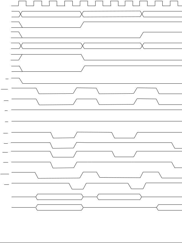
4. Write Cycle Timing Waveforms
On page 3-25, the M68300 write cycle timing diagram (Figure 3-12) shows incorrect timing for DS, UWE, and LWE. On page 3-28, the M68000 write cycle timing diagram (Figure 3-14) shows incorrect timing for AS68K, CSx, UDS/LDS, and UWE/LWE. Replace these figures with the following corrected figures.
5. Additional Note on MBAR Decode
Add to the CPU Space Cycles description on page 3-31: The CPU space decode logic allocates the 256-byte block from $3FF00-3FFFF to the SIM module. An internal 2-clock termination is provided by this initial decode for any access to this range, but selection of specific registers depends on additional decode.
Accesses to the MBAR register at long word $3FF00 are internal only, and are only visible by enabling show cycles. Users should directly access only the MBAR register, and use the LPSTOP instruction to generate the LPSTOP broadcast access to $3FFFE. The remaining address range $3FF04-3FFFD is Motorola reserved and should not be accessed.
This document contains information on a product under development. Motorola reserves the right to change or discontinue this product without notice.
SEMICONDUCTOR PRODUCT INFORMATION
MOTOROLA, 1995

S0 |
S2 |
S4 |
S0 |
S2 |
S4 |
S0 |
S2 |
S4 |
CLKOUT |
|
|
|
|
|
|
|
|
A31–A2 |
|
|
|
|
|
|
|
|
A1 |
|
|
|
|
|
|
|
|
A0 |
|
|
|
|
|
|
|
|
FC3–FC0 |
|
|
|
|
|
|
|
|
SIZ1 |
|
|
|
|
|
|
|
|
|
WORD |
|
|
|
BYTE |
|
|
|
SIZ0 |
|
|
|
|
|
|
|
|
R/W |
|
|
|
|
|
|
|
|
AS |
|
|
|
|
|
|
|
|
CSx |
|
|
|
|
|
|
|
|
DS |
|
|
|
|
|
|
|
|
AS68K |
|
|
|
|
|
|
|
|
UDS, LDS |
|
|
|
|
|
|
|
|
UWE |
|
|
|
|
|
|
|
|
LWE |
|
|
|
|
|
|
|
|
DSACK |
|
|
|
|
|
|
|
|
DTC |
|
|
|
|
|
|
|
|
D15–D8 |
|
OP2 |
|
|
OP3 |
|
|
|
D7–D0 |
|
OP3 |
|
|
|
|
|
OP3 |
 WORD WRITE
 BYTE WRITE
 BYTE WRITE

Figure 3-12. M68300 Write Cycle timing
MOTOROLA |
MC68341 USER’S MANUAL ADDENDUM |
2 |
S0 |
S2 |
S4 |
S0 |
S2 |
S4 |
S0 |
S2 |
LKOUT |
|
|
|
|
|
|
|
A31–A2 |
|
|
|
|
|
|
|
A1 |
|
|
|
|
|
|
|
A0 |
|
|
|
|
|
|
|
C3–FC0 |
|
|
|
|
|
|
|
SIZ1 |
|
|
|
|
|
|
|
|
|
WORD |
|
|
BYTE |
|
|
SIZ0 |
|
|
|
|
|
|
|
R/W |
|
|
|
|
|
|
|
AS68K |
|
|
|
|
|
|
|
CSx |
|
|
|
|
|
|
|
DS |
|
|
|
|
|
|
|
AS |
|
|
|
|
|
|
|
UDS |
|
|
|
|
|
|
|
LDS |
|
|
|
|
|
|
|
UWE |
|
|
|
|
|
|
|
LWE |
|
|
|
|
|
|
|
DSACK |
|
|
|
|
|
|
|
DTC |
|
|
|
|
|
|
|
D15–D8 |
|
OP2 |
|
|
|
OP3 |
|
D7–D0 |
|
OP3 |
|
|
|
|
OP3 |
 WORD WRITE
 BYTE WRITE
 BYTE WRITE
Figure 3-14. M68000 Write Cycle Timing
MOTOROLA |
MC68341 USER’S MANUAL ADDENDUM |
3 |

6. Additional Notes on CPU Space Address Encoding
On page 3-31, Figure 3-16, the BKPT field for the Breakpoint Acknowledge address encoding is on bits 4-2, and the T bit is on bit 1. The Interrupt Acknowledge LEVEL field is on bits 3-1.
7. Breakpoints
On page 3-31, the last paragraph implies that either a software breakpoint (BKPT instruction) or hardware breakpoint can be used to insert an instruction. As noted in the following paragraphs, only a software breakpoint can be used to insert an instruction on the breakpoint acknowledge cycle.
8. Interrupt Latency
Add to the Interrupt Acknowledge Bus Cycles section on page 3-36: Interrupt latency from IRQx assert to prefetch of the first instruction in the interrupt handler is about 37 clocks + worst case instruction length in clocks (using 2-clock memory and autovector termination). From the instruction timing tables, this gives 37+71 (DIVS.L with worst-case <fea>) = 108 clocks worst case interrupt latency time. For applications requiring shorter interrupt response time the latency can be reduced by using simpler addressing modes and/or avoiding use of longer instructions (specifically DIVS.L, DIVU.L, MUL.L).
9. Interrupt Hold Time and Spurious Interrupts
Add to the Interrupt Acknowledge Bus Cycles section on page 3-36: Level sensitive interrupts must remain asserted until the corresponding IACK cycle; otherwise, a spurious interrupt exception may result or the interrupt may be ignored entirely. This is also true for level sensitive external interrupts which are autovectored using either the AVEC signal or the AVEC register, since the SIM will not respond to an interrupt arbitration cycle on the IMB if the external interrupt at that level has been removed. External interrupts configured as edge sensitive only have to be held a minimum of 1.5 clocks - see section 4.3.5.8 PROGRAMMABLE INTERRUPT REGISTER (PIR).
Note that the level 7 interrupt is also level sensitive, and must be held until a level 7 IACK begins. The level 7 interrupt is unique in that it cannot be masked - another level 7 interrupt exception can be created after the IACK cycle by negating IRQ7 and reasserting, even though the interrupt mask level in the SR is now set to level 7.
10. Typos in IACK Cycle Timing Waveforms
On page 3-38, Figure 3-21, the text “VECTOR FROM 16-BIT PORT” should be on D7-D0, and “VECTOR FROM 8-BIT PORT” should be on D15-D8. The responding device returns the vector number on the least significant byte of the data port.
11. Additional Note on Internal Autovector Operation
Add to the Autovector Interrupt Acknowledge Cycle section on page 3-38: If an external interrupt level is autovectored either by the AVEC register programming or the external AVEC signal, an external IACK will be started and terminated internally. The interrupting device should not respond to this IACK in any way, or the resulting operation is undefined.
12. Additional Notes on Retry Termination
On page 3-42, Table 3-4: When HALT and BERR are asserted together in case #5 to force a retry of the current bus cycle, relative timing of HALT and BERR must be controlled to avoid inadvertently causing bus error ter-
MOTOROLA |
MC68341 USER’S MANUAL ADDENDUM |
4 |

mination case #3. This can be done by asserting HALT and BERR either synchronously to the clock to directly control which edge each is recognized on, or asynchronously with HALT asserted for time [spec 47A+spec 47B] ns before BERR to guarantee recognition on or before the same clock edge as BERR.
13. Active Negate on Bus Arbitration
The 68341 actively pulls up all tri-stateable bus pins other than the data bus before tristating them during bus arbitration. This pullup function is not guaranteed to result in spec VOH levels before tristating, but will help reduce rise time on these signals when using weak external bus pullups.
14. Additional Note on Bus Arbitration Priority
For the bus arbitration description beginning on page 3-49: The arbitration priority between possible bus masters for this device is external request via BR (highest priority), DMA, then CPU (lowest). The priority of DMA channels 1 and 2 relative to each other is selected by their respective MAID levels which must be unique.
15. Additional Note on Bus Arbitration and Operand Coherency
For the bus arbitration description beginning on page 3-49: Each bus master maintains operand coherency when a higher priority request is recognized. For example, a CPU write of a long-word operand to a byte port results in a sequence of four bus cycles to complete the operand transfer - the CPU will not release the bus until the completion of the fourth bus cycle. A single address DMA transfer is handled in a similar manner. For a dual address DMA transfer, the read and write portions are handled as separate operands, allowing arbitration between the read and write bus cycles. Also, if different port sizes are specified in the DMA configuration for the source and destination, arbitration can occur between each of the multiple operand accesses which must be made to the smaller port for each operand access to the larger port. The RMC read/write sequences for a TAS instruction is also indivisible to guarantee data coherency. Arbitration is allowed between each operand transfer of a multi-operand operation such as a MOVEM instruction or exception stacking.
16. Additional Notes on RESET Interaction with Current Bus Cycle
Add to the Reset Operation description beginning page 3-55:
Hardware resets are held off until completion of the current operand transfer in order to maintain operand coherency. The processor resets at the end of the bus cycle in which the last portion of the operand is transferred, or after the bus monitor has timed out. The bus monitor operates for this specific case whether it is enabled or not, for the period of time that the BMT bits are set to.
The following reset sources reset all internal registers to their reset state: external, POR, software watchdog, double bus fault, loss of clock. Execution of a RESET instruction resets the peripheral module registers with the exception of the MCR registers. The MCR register in each module, the SIM41 registers, and the CPU state are not affected by execution of a RESET instruction.
17. External Reset
On page 3-56, Figure 3-33, the RESET signal negates for two clocks between internal and external assertions, not one. Note that RESET is not actively negated, and its rise time is dependent on the pullup resistor used.
18. Power-On Reset
On page 3-57, Figure 3-34. Power-Up Reset Timing Diagram: CLKOUT is not gated by VCO lock or other internal control signals, and can begin toggling as soon as VCC is high enough for the internal logic to begin operating. For crystal mode and external clock with VCO mode, after the VCO frequency has reached an initial
MOTOROLA |
MC68341 USER’S MANUAL ADDENDUM |
5 |

stable value, the 328*TCLKIN delay is counted down, and VCO lock is set after completion of the 328 clock delay. For external clock mode without VCO, the 328*TCLKIN delay starts as soon as EXTAL clock transitions are recognized. See note for page11-3 for more POR information.
19. Internal IMB Arbitration
On page 4-6, first paragraph, change the first sentence to read “There are eight arbitration levels for the various bus masters on the MC68341 to access the inter-module bus (IMB).”
20. Additional Note for External Clock Mode with PLL
On page 4-9, Table 4-1, External Clock Mode with PLL: the PLL phase locks the CLKOUT falling edge to the falling edge of the EXTCLK input clock. Maximum skew between falling edges of the EXTCLK and CLKOUT signals is specified in the Section 12 Electrical Characteristics.
21. External Clock Mode Operation
The next-to-last paragraph on page 4-11 incorrectly states that the SYNCR V, W, X, Y, and Z bits can all affect the system frequency in external clock mode. In external clock mode only the V bit affects the system frequency, by selecting either EXTCLK or EXTCLK/2 as reference input to the phase comparator. The VCO frequency divided by 2 is used both for CLKOUT as well as the feedback input to the phase comparator. A reset forces V=0, resulting in an initial processor operating frequency of 1/2 the EXTCLK frequency.
For applications using external clock mode, the 32KHz crystal connected to EXTAL and XTAL is only required if the realtime clock function is needed - ground EXTAL if the RTC is not used. Also, the clock input on EXTCLK should be very clean when the 32KHz oscillator is used. Excessive undershoot or overshoot, as well as fast edge rates may result in coupling to the adjacent XTAL input, affecting operation of the 32kHz oscillator.
22. Recommended XFC Capacitor Values
On page 4-12, third paragraph, and page 11-2, last paragraph: The XFC capacitor recommendation of 0.01 F to 0.1 F applies specifically to crystal mode operation. When using external clock with VCO mode, for phase detector refernce frequencies > 1MHz start with a capacitance value of 10000pf/F_MHz. For example at 16.0MHz the recommended XFC capacitance is approximately 10000pf/16.0 = 625pf - choose the next higher standard value available.
23. CLKOUT and VCO Frequency Programming
On pages 4-13 and 4-14, the column for W=1:Z=0:X=1 is incorrect - the correct value for each entry in this column is 2x the frequency in the X=0 column immediately to the left. A corrected table is shown on the following pages. Note that although a complete table is shown for all W:X:Y:Z combinations, both CLKOUT and VCO frequency limits must be observed when programming the SYNCR. For example, a system operating frequency (CLKOUT) of 25.16MHz can be selected with W:X:Y:Z=1:1:23:1, resulting in a VCO frequency of 50.3MHz. However, programming W:X:Y:Z=1:0:47:1 to achieve the same system frequency would result in a VCO frequency of greater than 100MHz, which is outside the spec VCO frequency operating range.
24. Additional Note for Global Chip Select
On page 4-16, section 4.2.4.2: When operating as a global chip select, CS0 does not assert for accesses to either the MBAR or to internal peripheral module registers.
MOTOROLA |
MC68341 USER’S MANUAL ADDENDUM |
6 |
 Loading...