

Page 1

查询MC68LC302PU20供应商
Microprocessors and Memory
Technologies Group
MC68LC302
Low Power Integrated
Multiprotocol Processor
Reference Manual
Motorola reserves the right to make changes without further notice to any products herein. Motorola makes no warranty, representation or guarantee regarding
the suitability of its products for any particular purpose, nor does Motorola assume any liability arising out of the application or use of any product or circuit, and
specifically disclaims any and all liability, including without limitation consequential or incidental damages. "Typical" parameters can and do vary in different
applications. All operating parameters, including "T ypicals" must be validated for each customer application by customer's technical experts. Motorola does not
convey any license under its patent rights nor the rights of others. Motorola products are not designed, intended, or authorized for use as components in
systems intended for surgical implant into the body, or other applications intended to support or sustain life, or for any other application in which the failure of the
Motorola product could create a situation where personal injury or death may occur. Should Buyer purchase or use Motorola products for any such unintended
or unauthorized application, Buyer shall indemnify and hold Motorola and its officers, employees, subsidiaries, affiliates, and distributors harmless against all
claims, costs, damages, and expenses, and reasonable attorney fees arising out of, directly or indirectly, any claim of personal injury or death associated with
such unintended or unauthorized use, even if such claim alleges that Motorola was negligent regarding the design or manufacture of the part. Motorola and
are registered trademarks of Motorola, Inc. Motorola, Inc. is an Equal Opportunity/Affirmative Action Employer .
Literature Distribution Centers:
USA/EUROPE: Motorola Literature Distribution; P.O. Box 20912, Arizona 85036.
JAPAN: Nippon Motorola Ltd.; 4-32-1, Nishi-Gotanda, Shinagawa-ku, Tokyo 141 Japan.
ASIA-PACIFIC: Motorola Semiconductors H.K. Ltd.; Silicon Harbour Center, No. 2 Dai King Street, Tai Po Industrial Estate,
Page 2

PREFACE
The complete documentation package for the MC68LC302 consists of the MC68LC302RM/
MC68LC302 Low Power Integrated Multiprotocol Processor Reference Manual
AD,
M68000PM/AD,
MC68302 Integrated Multiprotocol Processor User’s Manual,
MC68LC302 Low Power Integrated Multiprotocol Processor Product Brief
MC68000 Family Programmer’s Reference Manual,
and the MC68LC302/D,
MC68302UM/AD,
.
,
MC68LC302 Low Power Integrated Multiprotocol Processor Reference Manual
The
scribes the programming, capabilities, registers, and operation of the MC68LC302 that differ
from the original MC68302; the
instruction details for the MC68LC302; and
tocol Processor Product Brief
MC68302 Integrated Multiprotocol Processor User’s Manual
The
MC68LC302
scribes the new features of the MC68LC302.
This user’s manual is organized as follows:
Section 1 Introduction
Section 2 Configuration, Clocking, Low Power Modes, and Internal Memory Map
Section 3 System Integration Block (SIB)
Section 4 Communications Processor (CP)
Section 5 Signal Description
Section 6 Electrical Characteristics
Section 7 Mechanical Data And Ordering Information
Low Power Integrated Multiprotocol Processor
MC68000 Family Programmer’s Reference Manual
the
MC68LC302 Low Power Integrated Multipro-
provides a brief description of the MC68LC302 capabilities.
is required, since the
Reference Manual
de-
provides
only de-
ELECTRONIC SUPPORT:
The Technical Support BBS, known as AESOP (Application Engineering Support Through
On-Line Productivity), can be reach by modem or the internet. AESOP provides commonly
asked application questons, latest device errata, device specs, software code, and many
other useful support functions.
Modem: Call 1-800-843-3451 (outside US or Canada 512-891-3650) on a modem that runs
at 14,400 bps or slower. Set your software to N/8/1/F emulating a vt100.
Internet: This access is provided by telneting to pirs.aus.sps.mot.com [129.38.233.1] or
through the World Wide Web at http://pirs.aus.sps.mot.com.
—
Sales Offices —
For questions or comments pertaining to technical information, questions, and applications,
please contact one of the following sales offices nearest you.
iii
MC68LC302 REFERENCE MANUAL
MOTOROLA
Page 3

iv
UNITED STATES
ALABAMA , Huntsville (205) 464-6800
ARIZONA , Tempe (602) 897-5056
CALIFORNIA , Agoura Hills (818) 706-1929
CALIFORNIA , Los Angeles (310) 417-8848
CALIFORNIA , Irvine (714) 753-7360
CALIFORNIA , Rosevllle (916) 922-7152
CALIFORNIA , San Diego (619) 541-2163
CALIFORNIA , Sunnyvale (408) 749-0510
COLORADO , Colorado Springs (719) 599-7497
COLORADO , Denver (303) 337-3434
CONNECTICUT , Wallingford (203) 949-4100
FLORIDA , Maitland (407) 628-2636
FLORIDA , Pompano Beach/
Fort Lauderdal (305) 486-9776
FLORIDA , Clearwater (813) 538-7750
GEORGlA , Atlanta (404) 729-7100
IDAHO , Boise (208) 323-9413
ILLINOIS , Chicago/Hoffman Estates (708) 490-9500
INDlANA , Fort Wayne (219) 436-5818
INDIANA , Indianapolis (317) 571-0400
INDIANA , Kokomo (317) 457-6634
IOWA , Cedar Rapids (319) 373-1328
KANSAS , Kansas City/Mission (913) 451-8555
MARYLAND , Columbia (410) 381-1570
BRITISH COLUMBIA , Vancouver (604) 293-7605
ONTARIO , Toronto (416) 497-8181
ONTARIO , Ottawa (613) 226-3491
QUEBEC , Montreal (514) 731-6881
AUSTRALIA , Melbourne (61-3)887-0711
AUSTRALIA , Sydney (61(2)906-3855
BRAZIL , Sao Paulo 55(11)815-4200
CHINA , Beijing 86 505-2180
FINLAND , Helsinki 358-0-35161191
Car Phone 358(49)211501
FRANCE , Paris/Vanves 33(1)40 955 900
GERMANY , Langenhagen/ Hanover 49(511)789911
GERMANY , Munich 49 89 92103-0
GERMANY , Nuremberg 49 911 64-3044
GERMANY , Sindelfingen 49 7031 69 910
GERMANY ,Wiesbaden 49 611 761921
HONG KONG , Kwai Fong 852-4808333
Tai Po 852-6668333
INDIA , Bangalore (91-812)627094
ISRAEL , Tel Aviv 972(3)753-8222
ITALY , Milan 39(2)82201
JAPAN , Aizu 81(241)272231
JAPAN , Atsugi 81(0462)23-0761
JAPAN , Kumagaya 81(0485)26-2600
JAPAN , Kyushu 81(092)771-4212
JAPAN , Mito 81(0292)26-2340
JAPAN , Nagoya 81(052)232-1621
JAPAN , Osaka 81(06)305-1801
JAPAN, Sendai 81(22)268-4333
JAPAN,
JAPAN,
JAPAN
KOREA , Pusan 82(51)4635-035
KOREA , Seoul 82(2)554-5188
Tachikawa 81(0425)23-6700
Tokyo 81(03)3440-3311
, Yokohama 81(045)472-2751
CANADA
INTERNATIONAL
MASSACHUSETTS , Marborough (508) 481-8100
MASSACHUSETTS , Woburn (617) 932-9700
MICHIGAN , Detroit (313) 347-6800
MINNESOTA , Minnetonka (612) 932-1500
MISSOURI , St. Louis (314) 275-7380
NEW JERSEY , Fairfield (201) 808-2400
NEW YORK , Fairport (716) 425-4000
NEW YORK , Hauppauge (516) 361-7000
NEW YORK , Poughkeepsie/Fishkill (914) 473-8102
NORTH CAROLINA , Raleigh (919) 870-4355
OHIO , Cleveland (216) 349-3100
OHIO , Columbus Worthington (614) 431-8492
OHIO , Dayton (513) 495-6800
OKLAHOMA , Tulsa (800) 544-9496
OREGON , Portland (503) 641-3681
PENNSYLVANIA , Colmar (215) 997-1020
Philadelphia/Horsham (215) 957-4100
TENNESSEE , Knoxville (615) 690-5593
TEXAS , Austin (512) 873-2000
TEXAS , Houston (800) 343-2692
TEXAS , Plano (214) 516-5100
VIRGINIA , Richmond (804) 285-2100
WASHINGTON , Bellevue (206) 454-4160
Seattle Access (206) 622-9960
WISCONSIN , Milwaukee/Brookfield (414) 792-0122
MALAYSIA , Penang 60(4)374514
MEXICO , Mexico City 52(5)282-2864
MEXICO , Guadalajara 52(36)21-8977
Marketing 52(36)21-9023
Customer Service 52(36)669-9160
NETHERLANDS , Best (31)49988 612 11
PUERTO RICO , San Juan (809)793-2170
SINGAPORE
SPAIN , Madrid 34(1)457-8204
or 34(1)457-8254
SWEDEN , Solna 46(8)734-8800
SWITZERLAND
SWITZERLAND, Zurich 41(1)730 4074
TAlWAN, Taipei 886(2)717-7089
THAILAND, Bangkok (66-2)254-4910
UNITED KINGDOM, Aylesbury 44(296)395-252
COLORADO, Grand Junction
Cheryl Lee Whltely (303) 243-9658
KANSAS, Wichita
Melinda Shores/Kelly Greiving (316) 838 0190
NEVADA, Reno
Galena Technology Group (702) 746 0642
NEW MEXICO, Albuquerque
S&S Technologies, lnc. (505) 298-7177
UTAH, Salt Lake City
Utah Component Sales, Inc. (801) 561-5099
WASHINGTON, Spokane
Doug Kenley (509) 924-2322
ARGENTINA, Buenos Aires
Argonics, S.A. (541) 343-1787
Elmo Semiconductor (818) 768-7400
Minco Technology Labs Inc. (512) 834-2022
Semi Dice Inc. (310) 594-4631
, Geneva 41(22)7991111
FULL LINE REPRESENTATIVES
HYBRID COMPONENTS RESELLERS
(65)2945438
MOTOROLA
MC68LC302 REFERENCE MANUAL
Page 4

TABLE OF CONTENTS
Paragraph Title Page
Number Number
Section 1
Introduction
1.1 Block Diagram......................................................................................... 1-1
1.2 Features.................................................................................................. 1-2
1.3 LC302 Applications................................................................................. 1-3
1.4 LC302 Differences .................................................................................. 1-3
Section 2
Configuration, Clocking, Low Power Modes, and Internal Memory Map
2.1 MC68LC302 and MC68302 Signal Differences...................................... 2-1
2.2 IMP Configuration Control....................................................................... 2-2
2.2.1 Base Address Register ...........................................................................2-4
2.3 System Configuration Registers.............................................................. 2-5
2.4 Clock Generation and Low Power Control.............................................. 2-5
2.4.1 PLL and Oscillator Changes to IMP........................................................ 2-5
2.4.1.1 Clock Control Register............................................................................ 2-6
2.4.2 MC68LC302 System Clock Generation.................................................. 2-6
2.4.2.1 Default System Clock Generation........................................................... 2-7
2.4.3 IMP System Clock Generation................................................................ 2-8
2.4.3.1 System Clock Configuration.................................................................... 2-8
2.4.3.2 On-Chip Oscillator................................................................................... 2-8
2.4.3.3 Phase-Locked Loop (PLL) ......................................................................2-9
2.4.3.4 Frequency Multiplication .........................................................................2-9
2.4.3.4.1 Low Power PLL Clock Divider............................................................... 2-10
2.4.3.4.2 IMP PLL and Clock Control Register (IPLCR) ......................................2-10
2.4.3.5 IMP Internal Clock Signals.................................................................... 2-12
2.4.3.5.1 IMP System Clock................................................................................. 2-12
2.4.3.5.2 BRG Clock ............................................................................................2-12
2.4.3.5.3 PIT Clock............................................................................................... 2-12
2.4.3.6 IMP PLL Pins ........................................................................................2-12
2.4.3.6.1 VCCSYN............................................................................................... 2-12
2.4.3.6.2 GNDSYN............................................................................................... 2-12
2.4.3.6.3 XFC....................................................................................................... 2-12
2.4.3.6.4 MODCLK............................................................................................... 2-12
2.4.4 IMP Power Management....................................................................... 2-13
2.4.4.1 IMP Low Power Modes......................................................................... 2-13
2.4.4.1.1 STOP Mode ..........................................................................................2-13
2.4.4.1.2 DOZE Mode.......................................................................................... 2-13
2.4.4.1.3 STAND_BY Mode................................................................................. 2-13
MOTOROLA
MC68LC302 REFERENCE MANUAL
v
Page 5

vi
Table of Contents
Paragraph Title Page
Number Number
2.4.4.1.4 SLOW_GO Mode...................................................................................2-14
2.4.4.1.5 NORMAL Mode......................................................................................2-14
2.4.4.1.6 IMP Operation Mode Control Register (IOMCR) ...................................2-14
2.4.4.1.7 Low Power Drive Control Register (LPDCR).........................................2-15
2.4.4.1.8 IMP Power Down Register (IPWRD) .....................................................2-15
2.4.4.1.9 Default Operation Modes.......................................................................2-15
2.4.4.2 Low Power Support................................................................................2-15
2.4.4.2.1 Enter the SLOW_GO mode...................................................................2-15
2.4.4.2.2 Entering the STOP/ DOZE/ STAND_BY Mode......................................2-16
2.4.4.2.3 IMP Wake-Up from Low Power STOP Modes.......................................2-17
2.4.4.2.4 IMP Wake-Up Control Register (IWUCR)..............................................2-17
2.4.4.3 Fast Wake-Up........................................................................................2-18
2.4.4.3.5 Ring Oscillator Control Register (RINGOCR)........................................2-19
2.4.4.3.6 Ring Oscillator Event Register (RINGOEVR). .......................................2-20
2.5 MC68LC302 Dual Port RAM..................................................................2-20
2.6 Internal Registers map...........................................................................2-23
Section 3
System Integration Block (SIB)
3.1 System Control ........................................................................................3-1
3.1.1 System Control Register (SCR)...............................................................3-2
3.1.2 System Status Bits...................................................................................3-3
3.1.3 System Control Bits .................................................................................3-3
3.1.4 Freeze Control.........................................................................................3-5
3.1.5 Hardware Watchdog................................................................................3-5
3.2 Programmable Data Bus Size Switch......................................................3-6
3.2.1 Bus Switch Register (BSR)......................................................................3-6
3.2.2 Basic Procedure:......................................................................................3-6
3.3 Load Boot Code from An SCC.................................................................3-7
3.4 DMA Control ..........................................................................................3-10
3.4.1 MC68LC302 Differences........................................................................3-10
3.4.2 IDMA Registers (Independent DMA Controller).....................................3-11
3.4.2.1 Channel Mode Register (CMR)..............................................................3-11
3.4.2.2 Source Address Pointer Register (SAPR) .............................................3-13
3.4.2.3 Destination Address Pointer Register (DAPR).......................................3-13
3.4.2.4 Function Code Register (FCR) ..............................................................3-13
3.4.2.5 Byte Count Register (BCR)....................................................................3-13
3.4.2.6 Channel Status Register (CSR).............................................................3-13
3.5 Interrupt Controller.................................................................................3-14
3.5.1 Interrupt Controller Key Differences.......................................................3-14
3.5.2 Interrupt Controller Programming Model................................................3-14
3.5.2.1 Global Interrupt Mode Register (GIMR).................................................3-14
3.5.2.2 Interrupt Pending Register (IPR)............................................................3-15
3.5.2.3 Interrupt Mask Register (IMR)................................................................3-16
3.5.2.4 Interrupt In-Service Register (ISR).........................................................3-16
MC68LC302 REFERENCE MANUAL
MOTOROLA
Page 6

Table of Contents
Paragraph Title Page
Number Number
3.6 Parallel I/O Ports................................................................................... 3-17
3.6.1 Parallel I/O Port Differences.................................................................. 3-17
3.6.2 Port A .................................................................................................... 3-17
3.6.3 Port B .................................................................................................... 3-18
3.6.3.1 PB7–PB3...............................................................................................3-18
3.6.3.2 PB11–PB8.............................................................................................3-18
3.6.4 Port N....................................................................................................3-19
3.6.5 Port Registers........................................................................................3-19
3.7 Timers................................................................................................... 3-20
3.7.1 MC68LC302 General Purpose Timer Difference .................................. 3-20
3.7.2 General Purpose Timers Programming Mode.......................................3-20
3.7.2.1 Timer Mode Register (TMR1, TMR2)....................................................3-20
3.7.2.2 Timer Reference Registers (TRR1, TRR2)...........................................3-21
3.7.2.3 Timer Capture Registers (TCR1, TCR2)............................................... 3-21
3.7.2.4 Timer Counter (TCN1, TCN2)...............................................................3-21
3.7.2.5 Timer Event Registers (TER1, TER2)................................................... 3-21
3.7.3 Timer 3 - Software Watchdog Timer ..................................................... 3-22
3.7.3.1 Software Watchdog Reference Register (WRR)................................... 3-22
3.7.3.2 Software Watchdog Counter (WCN).....................................................3-22
3.7.4 Periodic Interrupt Timer (PIT)................................................................3-22
3.7.4.1 Overview ............................................................................................... 3-23
3.7.4.2 Periodic Timer Period Calculation......................................................... 3-23
3.7.4.3 Using the Periodic Timer As a Real-Time Clock...................................3-24
3.7.4.4 Periodic Interrupt Timer Register (PITR)...............................................3-24
3.8 External Chip-Select Signals and Wait-State Logic.............................. 3-25
3.8.1 Chip-Select Registers............................................................................3-26
3.8.1.1 Base Register (BR3–BR0) .................................................................... 3-26
3.8.1.2 Option Registers (OR3–OR0) ............................................................... 3-26
3.8.2 Disable CPU Logic (M68000)................................................................ 3-28
3.8.3 Bus Arbitration Logic.............................................................................3-28
3.8.3.1 Internal Bus Arbitration..........................................................................3-28
3.8.3.2 External Bus Arbitration......................................................................... 3-28
3.9 Dynamic RAM Refresh Controller......................................................... 3-29
Section 4
Communications Processor (CP)
4.1 MC68LC302 Key Differences from the MC68302...................................4-1
4.2 Serial Channels Physical Interface..........................................................4-2
4.2.1 Serial Interface Registers........................................................................ 4-2
4.2.1.1 Serial Interface Mode Register (SIMODE)..............................................4-2
4.2.1.2 Serial Interface Mask Register (SIMASK)...............................................4-4
4.3 Serial Communication Controllers (SCCs)..............................................4-4
4.3.1 SCC Configuration Register (SCON)......................................................4-4
4.3.1.1 Divide by 2 Input Blocks (New Feature).................................................. 4-4
4.3.2 Disable SCC1 Serial Clocks Out (DISC)................................................. 4-4
4.3.2.1 RCLK1 and TCLK1 Pin Options.............................................................. 4-5
MOTOROLA
MC68LC302 REFERENCE MANUAL
vii
Page 7

Table of Contents
Paragraph Title Page
Number Number
4.3.3 SCC Mode Register (SCM)......................................................................4-5
4.3.4 SCC Data Synchronization Register (DSR).............................................4-6
4.3.5 Buffer Descriptors Table..........................................................................4-6
4.3.6 SCC Parameter RAM Memory Map.........................................................4-7
4.3.7 Interrupt Mechanism................................................................................4-7
4.3.8 UART Controller.......................................................................................4-7
4.3.8.1 UART Memory Map.................................................................................4-7
4.3.8.2 UART Mode Register...............................................................................4-8
4.3.8.3 UART Receive Buffer Descriptor (Rx BD) ...............................................4-8
4.3.8.4 UART Transmit Buffer Descriptor (Tx BD)...............................................4-8
4.3.8.5 UART Event Register...............................................................................4-9
4.3.8.6 UART MASK Register..............................................................................4-9
4.3.9 Autobaud Controller (New) ......................................................................4-9
4.3.9.1 Autobaud Channel Reception Process....................................................4-9
4.3.9.2 Autobaud Channel Transmit Process....................................................4-11
4.3.9.3 Autobaud Parameter RAM.....................................................................4-11
4.3.9.4 Autobaud Programming Model..............................................................4-13
4.3.9.4.1 Preparing for the Autobaud Process......................................................4-13
4.3.9.4.2 Enter_Baud_Hunt Command.................................................................4-14
4.3.9.4.3 Autobaud Command Descriptor.............................................................4-14
4.3.9.4.4 Autobaud Lookup Table.........................................................................4-15
4.3.9.5 Lookup Table Example..........................................................................4-17
4.3.9.6 Determining Character Length and Parity..............................................4-17
4.3.9.7 Autobaud Reception Error Handling Procedure.....................................4-18
4.3.9.8 Autobaud Transmission.........................................................................4-18
4.3.9.8.1 Automatic Echo......................................................................................4-19
4.3.9.8.2 Smart Echo............................................................................................4-19
4.3.9.9 Reprogramming to UART Mode or Another Protocol ............................4-20
4.3.10 HDLC Controller.....................................................................................4-20
4.3.10.1 HDLC Memory Map...............................................................................4-20
4.3.10.2 HDLC Mode Register.............................................................................4-20
4.3.10.3 HDLC Receive Buffer Descriptor (Rx BD) .............................................4-21
4.3.10.4 HDLC Transmit Buffer Descriptor (Tx BD).............................................4-21
4.3.10.5 HDLC Event Register.............................................................................4-21
4.3.10.6 HDLC Mask Register.............................................................................4-21
4.3.11 BISYNC Controller.................................................................................4-22
4.3.11.1 BISYNC Memory Map............................................................................4-22
4.3.11.2 BISYNC Mode Register.........................................................................4-22
4.3.11.3 BISYNC Receive Buffer Descriptor (Rx BD)..........................................4-22
4.3.11.4 BISYNC Transmit Buffer Descriptor (Tx BD).........................................4-22
4.3.11.5 BISYNC Event Register.........................................................................4-23
4.3.11.6 BISYNC Mask Register..........................................................................4-23
4.3.12 Transparent Controller...........................................................................4-23
4.3.12.1 Transparent Memory Map......................................................................4-23
4.3.12.2 Transparent Mode Register...................................................................4-24
viii
MC68LC302 REFERENCE MANUAL
MOTOROLA
Page 8

Table of Contents
Paragraph Title Page
Number Number
4.3.12.3 Transparent Receive Buffer Descriptor (RxBD).................................... 4-24
4.3.12.4 Transparent Transmit Buffer Descriptor (Tx BD)...................................4-25
4.3.12.5 Transparent Event Register.................................................................. 4-25
4.3.12.6 Transparent Mask Register...................................................................4-25
4.4 Serial Communication Port (SCP)......................................................... 4-25
4.4.1 SCP Programming Model......................................................................4-25
4.4.2 SCP Transmit/Receive Buffer Descriptor.............................................. 4-26
4.5 Serial Management Controllers (SMCs)................................................4-26
4.5.1 SMC Programming Model..................................................................... 4-26
4.5.2 SMC Memory Structure and Buffers Descriptors..................................4-26
4.5.2.1 SMC1 Receive Buffer Descriptor .......................................................... 4-26
4.5.2.2 SMC1 Transmit Buffer Descriptor ......................................................... 4-26
4.5.2.3 SMC2 Receive Buffer Descriptor .......................................................... 4-27
4.5.2.4 SMC2 Transmit Buffer Descriptor ......................................................... 4-27
Section 5
Signal Description
5.1 Functional Groups...................................................................................5-1
5.2 Power Pins.............................................................................................. 5-2
5.3 Clock Pins............................................................................................... 5-4
5.4 System Control Pins................................................................................ 5-5
5.5 Address Bus Pins (A19–A1).................................................................... 5-7
5.6 Data Bus Pins (D15—D0)....................................................................... 5-8
5.7 Bus Control Pins......................................................................................5-9
5.8 Bus Arbitration Pins............................................................................... 5-10
5.9 Interrupt Control Pins............................................................................ 5-11
5.10 MC68LC302 Bus Interface Signal Summary......................................... 5-12
5.11 Physical Layer Serial Interface Pins......................................................5-14
5.12 Typical Serial Interface Pin Configurations ........................................... 5-14
5.13 NMSI1 or ISDN Interface Pins............................................................... 5-14
5.14 NMSI2 Port or Port a Pins..................................................................... 5-17
5.15 PAIO / SCP Pins ................................................................................... 5-18
5.16 Timer Pins.............................................................................................5-19
5.17 Parallel I/O Pins with Interrupt Capability.............................................. 5-20
5.18 Chip-Select Pins....................................................................................5-21
5.19 When to Use Pullup Resistors............................................................... 5-21
Section 6
Electrical Characteristics
6.1 Maximum Ratings....................................................................................6-2
6.2 Thermal Characteristics.......................................................................... 6-2
6.3 Power Considerations............................................................................. 6-3
6.4 Power Dissipation....................................................................................6-4
6.5 DC Electrical Characteristics................................................................... 6-5
6.6 DC Electrical Characteristics—NMSI1 in IDL Mode................................ 6-6
6.7 AC Electrical Specifications—Clock Timing............................................ 6-6
MOTOROLA
MC68LC302 REFERENCE MANUAL
ix
Page 9

x
Table of Contents
Paragraph Title Page
Number Number
6.7.1 AC Electrical Characteristics - IMP Phased Lock Loop (PLL)
Characteristics.........................................................................................6-7
6.8 AC Electrical Specifications—IMP Bus Master Cycles............................6-8
6.9 AC Electrical Specifications—DMA .......................................................6-13
6.10 AC Electrical Specifications—External Master
Internal Asynchronous Read/Write Cycles ............................................6-16
6.11 AC Electrical Specifications—External Master Internal Synchronous
Read/Write Cycles.................................................................................6-19
6.12 AC Electrical Specifications—Internal Master Internal Read/Write
Cycles....................................................................................................6-23
6.13 AC Electrical Specifications—Chip-Select Timing Internal Master .......6-24
6.14 AC Electrical Specifications—Chip-Select Timing External Master.......6-25
6.15 AC Electrical Specifications—Parallel I/O .............................................6-26
6.16 AC Electrical Specifications—Interrupts ...............................................6-26
6.17 AC Electrical Specifications—Timers.....................................................6-28
6.18 AC Electrical Specifications—Serial Communications Port...................6-29
6.19 AC Electrical Specifications—IDL Timing).............................................6-30
6.20 AC Electrical Specifications—GCI Timing .............................................6-32
6.21 AC Electrical Specifications—PCM Timing............................................6-34
6.22 AC Electrical Specifications—NMSI Timing...........................................6-36
Section 7
Mechanical Data and Ordering Information
7.1 Pin Assignments......................................................................................7-1
7.1.1 Pin Grid Array (PGA) ...............................................................................7-1
7.1.2 Surface Mount (TQFP )............................................................................7-2
7.2 Package Dimensions...............................................................................7-3
7.2.1 Pin Grid Array (PGA) ...............................................................................7-3
7.2.2 Surface Mount (TQFP).............................................................................7-4
7.3 Ordering Information................................................................................7-5
MC68LC302 REFERENCE MANUAL
MOTOROLA
Page 10
SECTION 1
INTRODUCTION
Motorola has developed a low-cost version of the well-known MC68302 integrated multiprotocol processor (IMP) called the MC68LC302. Simply put, the LC302 is a traditional 68302
minus the third serial communication controller (SCC3) and has a new static 68000 core, a
new timer and low power modes. It is packaged in a low profile 100 TQFP that reduces
board space from the regular 68302, as well as making it suitable for use in height restricted
applications such as PCMCIA.
The document fully describes all the differences between the LC302 and the regular 68302.
Any feature not described in this document will operate as described in the
Manual
. In addition this document contains the full set of electrical descriptions for the
LC302, even though most of them are exactly the same as the 68302.
MC68302 User’s
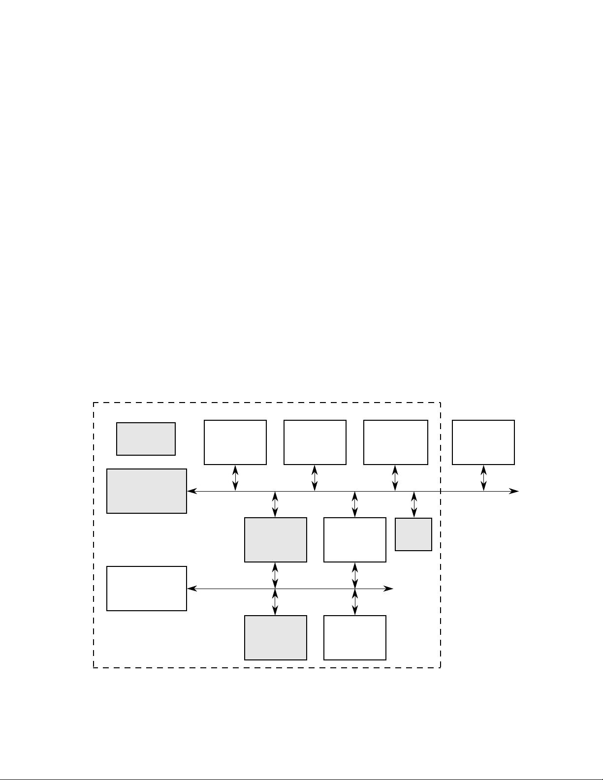
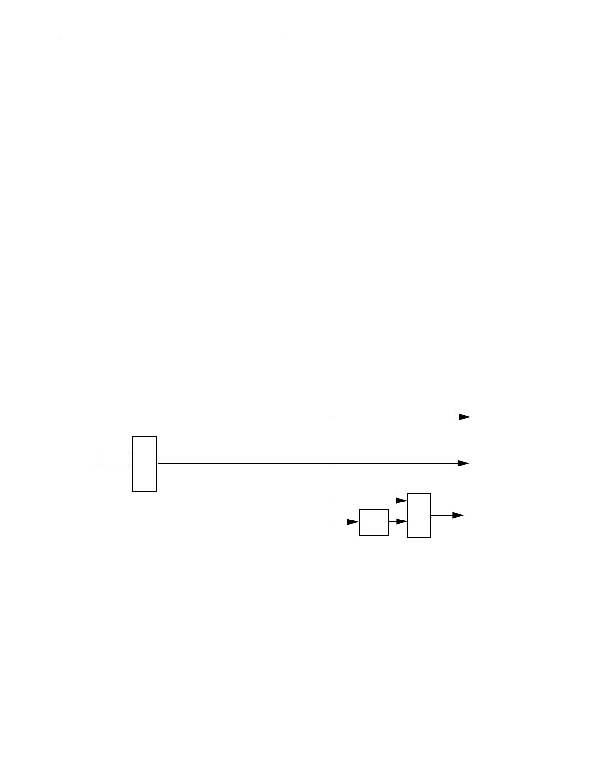
1.1 BLOCK DIAGRAM
The block diagram is shown in Figure 1-1.
LOW
POWER
CONTROL
STATIC
M68000
CORE
RISC
CONTROLLER
68LC302
INTERRUPT
CONTROLLER
4 SDMA
CHANNELS
2 SERIAL
CHANNELS
(SCCs)
1 GENERAL-
PURPOSE
DMA
CHANNEL
SYSTEM BUS
PERIPHERAL BUS
68000
1152 BYTES
DUAL-PORT
RAM
SCP
+
2 SMCs
3 TIMERS
4 CHIP SELECTS
PIO
SYSTEM CONTROL
PIT
RAM / ROM
20 ADDRESS
8/16 DATA
MOTOROLA
Figure 1-1. MC68LC302 Block Diagram
MC68LC302 REFERENCE MANUAL
1-1
Page 11

Introduction
1.2 FEATURES
The features of the LC302 are as follows. The items in bold face type show major differences from the MC68302, although a complete list of differences is given in 1.4 LC302 Differences.
• On-Chip
Static 68000 Core Supporting a 16- or 8-Bit M68000 Family-System
• SIB Including:
Independent Direct Memory Access (IDMA) Controller.
Interrupt Controller with Two Modes of Operation
Parallel Input/Output (I/O) Ports, some with Interrupt Capability
Parallel Input/Output (I/O) Ports on D15-D8 in 8 bit mode
On-Chip 1152-Byte Dual-Port RAM
Three Timers Including a Watchdog Timer
New Periodic Interrupt Timer (PIT)
Four Programmable Chip-Select Lines with Wait-State Generator Logic
Programmable Address Mapping of the Dual-Port RAM and IMP Registers
On-Chip Clock Generator with Output Signal
On-Chip PLL Allows Operation with 32kHz or 4MHz Crystals
Glueless Interface to EPROM, SRAM, Flash EPROM, and EEPROM
Allows Boot in 8-bit Mode, and Running Switch to 16-bit Mode
System Control:
System Status and Control Logic
Disable CPU Logic (Slave Mode Operation)
Hardware Watchdog
New Low-Power (Standby) Modes With Wake-up From 2 Pins or PIT
Freeze Control for Debugging (Available Only in the PGA Package)
DRAM Refresh Controller
• CP Including:
Main Controller (RISC Processor)
Two Independent Full-Duplex Serial Communications Controllers (SCCs)
Supporting Various Protocols:
High-Level/Synchronous Data Link Control (HDLC/SDLC)
Universal Asynchronous Receiver Transmitter (UART)
Binary Synchronous Communication (BISYNC)
Transparent Modes
Autobaud Support Instead of DDCMP and V.110
Boot from SCC Capability
1-2
MC68LC302 REFERENCE MANUAL
MOTOROLA
Page 12

Introduction
Four Serial DMA Channels for the Two SCCs
Flexible Physical Interface Accessible by SCCs Including:
Motorola Interchip Digital Link (IDL)
General Circuit Interface (GCI, Also Known as IOM
1
-2)
Pulse Code Modulation (PCM) Highway Interface
Nonmultiplexed Serial Interface (NMSI) Implementing Standard
Modem Signals
SCP for Synchronous Communication
Two Serial Management Controllers (SMCs) To Support IDL and GCI Auxiliary
Channels
• 100 Pin Thin Quad Flat Pack (TQFP) Packaging
1.3 LC302 APPLICATIONS
The LC302 excels in several applications areas.
First, any application using the 68302, but not needing all three serial channels is a potential
candidate for the LC302. Note however, that the LC302 sacrifices most of the provision for
external bus mastership, thus the LC302 may not be appropriate where the 68302 is used
as part of larger systems.
Second, the LC302 excels in low power and portable applications. The inclusion of a static
68000 core coupled with the low power modes built into the device make it ideal for handheld, or other low power applications. The new 32 kHz or 4 MHz PLL option greatly reduces
the total power budget of the designer’s board, and allows the LC302 to be an effective
device in low power systems. The LC302 can then optionally generate a full frequency clock
for use by the rest of the board. During low power modes, the new periodic interrupt timer
(PIT) allows the device to be woken up at regular intervals. In addition, two pins allow the
device to be woken up from low power modes.
Third, given that the LC302 is packaged in a 100TQFP package, it allows the 68302 to be
used in space critical applications, as well as height critical applications such as PCMCIA
cards.
Fourth, since the disable CPU mode (also known as slave mode) is still retained, the LC302
can function as a fully intelligent DMA-driven peripheral chip containing serial channels, timers, and chip selects, etc.
1.4 LC302 DIFFERENCES
The LC302 has some specific differences from the 68302. Most of these differences simply
result from the reduction in pins from 132 on the original 68302, to 100 pins on the LC302.
1.
IOM is a trademark of Siemens AG
MOTOROLA
MC68LC302 REFERENCE MANUAL
1-3
Page 13

Introduction
The following features have been removed or modified from the 68302 in order to make the
LC302 possible.
• SCC3 and its baud rate generator (BRG3) are removed.
• External masters are not able to take the bus away from the LC302 except through a
simple scheme using the HALT pin. This restriction does not apply to using the LC302
in CPU disabled mode (slave mode), in which case BR, BG, and BGACK are all available (they replace the IPL2-0 pins).
• Although the Independent DMA (IDMA) is still available, the external IDMA request pins
(DREQ, DACK, and DONE) have been eliminated.
• Four address lines have been eliminated, giving a total of 20 address lines. However,
the LC302 supports more than a 1 MB addressing range, since each of the four chip
selects still decodes a 24-bit address. This allows a total of 4 MB to be addressed.
• Since the function code pins and AVEC have been removed, interrupt acknowledgment
to external devices is only provided on levels one, six, and seven.
• The DDCMP and V.110 protocols have been removed.
†
• The total list of pins removed is: A23-A20, FC2-FC0
, AVEC
BG, BGACK, BCLR, IACK1, IACK6, IACK7, DREQ, DACK, DONE, BRG1, FRZ
†
, RMC, IAC
†
, BERR, BR,
†
,
TOUT1, NC1, NC3, TCLK3, RTS3, CTS3, CD3, plus 5 power and ground pins.
NOTE
Signals marked with
†
are available in the PGA Package.
• The SCP pins are now muxed with PA8, PA9, and PA10. The TXD3, RXD3, and RCLK3
functions associated with SCC3 are eliminated.
• The UDS, LDS, and R/W pins are not available except in slave mode, where they replace the WEH, WEL, and OE pins. Instead, the new pins WEH, WEL, and OE have
been defined for glueless interfacing to memory.
• PA12 is now muxed with the MODCLK pin, which is associated with the 32 kHz or 4
MHz PLL. The MODCLK pin is sampled after reset, and then becomes PA12.
• New VCCsyn, GNDsyn, and XFC pins have been added in support of the on-chip PLL.
• For purposes of emulation support only, a special 132 PGA version is supported. This
version adds back the FC2-0, IAC, FRZ, and AVEC pins. The FC2-0 pins allow bus cycles to be distinguished between program and data accesses, interrupt cycles, etc. The
IAC, FRZ, and AVEC pins are provided so that emulation vendors can quickly retrofit
their existing 68302 emulator designs to support the LC302.
1-4
MC68LC302 REFERENCE MANUAL
MOTOROLA
Page 14

SECTION 2
CONFIGURATION, CLOCKING, LOW POWER MODES,
AND INTERNAL MEMORY MAP
The MC68LC302 integrates a high-s/peed M68000 processor with multiple communications
peripherals. The provision of direct memory access (DMA) control and link layer management with the serial ports allows high throughput of data for communications-intensive applications, such as basic rate Integrated Services Digital Network (ISDN).
The MC68LC302 can operate either in the full MC68000 mode with a 16-bit data bus or in
the MC68008 mode with an 8-bit data bus by connecting the bus width (BUSW) pin low.
NOTE
The BUSW pin is static and is not intended to be used for dynamic bus sizing. Instead the BSW and BSWEN bits in the BSR
register should be used to switch the bus width after reset (3.2
Programmable Data Bus Size Switch). If the state of the BUSW
pin is changed during operation of the MC68LC302, erratic operation may occur.
Refer to the MC68000UM/AD,
the MC68302UM/AD,
plete details of the on-chip microprocessor including the programming model and instruction
set summary. Throughout this manual, references may use the notation M68000, meaning
all devices belonging to this family of microprocessors, or the notation MC68000, MC68008,
meaning the specific microprocessor products.
This section is intended to describe configuration of the MC68LC302 and the differences
between theLC302 and the MC68000 and the MC68302.This section also includes tables
that show the registers of the IMP portion of the MC68LC302. All of the registers are memory
mapped into the 68000 space
MC68302 Integrated Multiprotocol Processor User’s Manual
M68000 8-/16-/32-Bit Microprocessors User's Manual
, and
, for com-
2.1 MC68LC302 AND MC68302 SIGNAL DIFFERENCES
The MC68LC302 in CPU enable mode has Write Enable (WE) signals instead of UDS and
LDS signal. The Write Enable High (WEH
will be accessed, and the Write Enable Low (WEL
data byte will be accessed. When the core is disabled, WEH
A0 and LDS/DS respectively.
MOTOROLA
MC68LC302 REFERENCE MANUAL
/A0) signal indicates that most significant data byte
/DS) indicates that the least significant
/A0 and WEL/DS become UDS/
2-1
Page 15

Configuration, Clocking, Low Power Modes, and Internal Memory Map
The MC68LC302 in CPU enable mode has an output enable (OE) signal instead of R/W.
The OE
the data bus. When the core is disabled, OE
signal indicates that the MC68LC302 expects an external device to drive data onto
becomes the R/W signal.
The MC68LC302 in CPU enable mode does not have BR
the HALT
pin is used to force the MC68LC302 off of the bus (see the HALT signal descrip-
, BG, and BGACK pins. Instead
tion in 5.4 System Control Pins). While the MC68LC302 is halted, the chip selects are still
functional. The external master will not be able to access the internal registers and dual-port
RAM.
When the core is disabled, the IPL0
, IPL1, and IPL2 lines become the BR, BG, and BGACK
signals. The only external interrupts handled are PB8, PB9, PB10, and PB11.
Two M6800 signals are omitted from the 68LC302: valid memory address (VMA
(E). The valid peripheral address (VPA
) signal which was used on the MC68302 as AVEC
) and enable
has been removed from the MC68LC302.
The signals for the serial communications port (SCP) have been multiplexed with the PA8,
PA9, and PA10 pins and the signals for SCC3 have been removed.
The FC2-0 pins have been removed from the MC68LC302. These signals are still driven
internally by the core depending on the type of bus cycle (i.e. supervisor program space,
supervisor data space, etc.) and the internal peripherals. They can still be used for address
comparison in the chip select registers. In disable CPU mode and when HALT
is asserted
for external masters, the FC signals are internally driven to 5 for external master accesses
to internal peripherals.
The A23-A20 pins have been removed from the MC68LC302. These signals are still driven
internally by the core and the internal peripherals. The user must program the full 24-bit
address in the chip select base registers, option registers, and in the pointers used by the
internal DMA and SCCs. In disable CPU mode and when HALT
is asserted for external mas-
ters, the A23-20 signals are driven to zero for all external master accesses.
The other signals removed from the MC68LC302 are IAC, RMC
DREQ
TOUT1
/PA13, DACK/PA14, DONE/PA15, IACK7/PB0, IACK6/PB1, IACK7/PB2, and
/PB4.
, BLCR, BERR, FRZ, BRG1,
The signals XFC and MODCLK (multiplexed with PA12) have been added for use with the
on-chip phase lock loop.
For purposes of emulation support only, a special 132 PGA version is supported. This version adds back the FC2-0, IAC, F
RZ, and AVEC pins.
2.2 IMP CONFIGURATION CONTROL
A number of reserved entries in the external M68000 exception vector table are used as
addresses for the internal system configuration registers. See Table 2-1.
2-2
MC68LC302 REFERENCE MANUAL
MOTOROLA
Page 16
Configuration, Clocking, Low Power Modes, and Internal Memory Map
The BAR entry contains the BAR described in this section. The SCR entry contains the SCR
described in Section 3 System Integration Block (SIB).
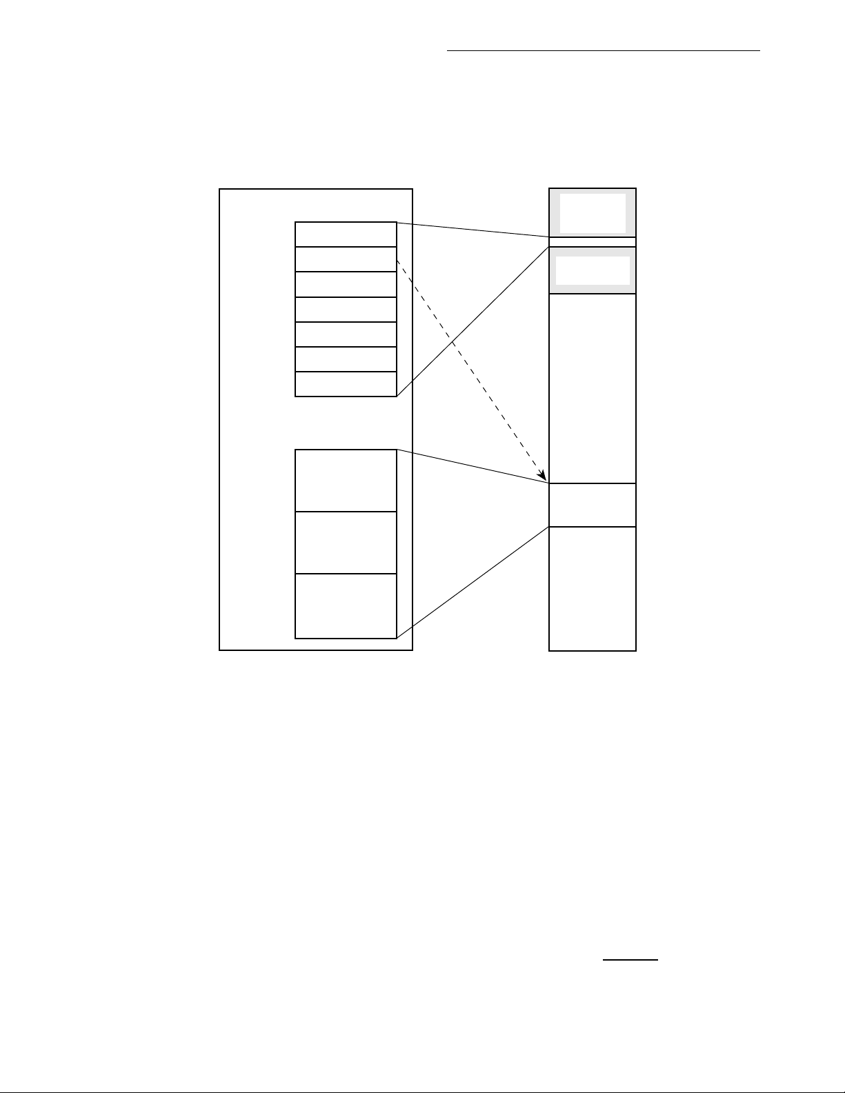
Figure 2-1 shows all the IMP on-chip addressable locations and how they are mapped into
system memory.
SYSTEM MEMORY MAP
$0
EXCEPTION
VECTOR
TABLE
$0F0
IMP
PITR
$0F2
$0F4
$0F7
$0F8
$0FA
$0FB
BASE + $0
BASE + $400
BASE + $800
BASE + $FFF
BAR ENTRY
SCR ENTRY
WAKE-UP
IMP PLL
IMP MODE CONTROL
IMP POWER DOWN
4K BLOCK
SYSTEM RAM
(DUAL-PORT)
PARAMETER RAM
(DUAL-PORT)
INTERNAL
REGISTERS
$3FF
BAR
POINTS
TO THE
BASE
$xxx000 = BASE
$FFFFFF
256 VECTOR
ENTRIES
4K BLOCK
Figure 2-1. IMP Configuration Control
The on-chip peripherals, including those peripherals in both the communications processor
(CP) and system integration block (SIB), require a 4K-byte block of address space. This 4Kbyte block location is determined by writing the intended base address to the BAR in supervisor data space (FC = 5). The FC2-0 pins are internally driven by the MC68LC302 to supervisor data space.
After a total system reset, the on-chip peripheral base address is undefined, and it is not
possible to access the on-chip peripherals at any address until BAR is written. The BAR and
the SCR can always be accessed at their fixed addresses.
NOTE
The BAR and SCR registers are internally reset only when a total system reset occurs by the simultaneous assertion of RESET
MOTOROLA
MC68LC302 REFERENCE MANUAL
2-3
Page 17

Configuration, Clocking, Low Power Modes, and Internal Memory Map
and
HALT. The chip-select (CS) lines are not asserted on ac-
cesses to these locations. Thus, it is very helpful to use CS
lines
to select external ROM/RAM that overlaps the BAR and SCR
register locations, since this prevents potential bus contention.
NOTE
In 8-bit system bus operation, IMP accesses are not possible until the low byte of the BAR is written. Since the MOVE.W instruction writes the high byte followed by the low byte, this instruction
guarantees the entire word is written.
Do not assign other devices on the system bus an address that falls within the address
range of the peripherals defined by the BAR. If this happens, an internal BERR
is generated
to the core (if the address decode conflict enable (ADCE) bit is set) and the address decode
conflict (ADC) bit in the SCR is set.
2.2.1 Base Address Register
The BAR is a 16-bit, memory-mapped, read-write register consisting of the high address
bits, the compare function code bit, and the function code bits. Upon a total system reset, its
value may be read as $BFFF, but its value is not valid until written by the user. The address
of this register is fixed at $0F2 in supervisor data space. BAR cannot be accessed in user
data space.
15 13 12 11 0
FC2–FC0 CFC
23 22 21 20 19 18 17 16 15 14 13 12
BASE ADDRESS
Bits 15–13—FC2–FC0
The FC2–FC0 field is contained in bits 15–13 of the BAR. These bits are used to set the
address space of 4K-byte block of on-chip peripherals. The address compare logic uses
these bits, dependent upon the CFC bit, to cause an address match within its address
space. When the core is enabled, the function code bits will be driven by the core to indicate the type of cycle in process. In disable CPU mode, the FC pins are not present and
are internally driven to 5. Since, the user does not have any control over how the FC signals are driven, it is recommended that the user write these bits to zero and write the CFC
bit to zero to disable the FC comparison.
NOTE
Do not assign this field to the M68000 core interrupt acknowledge space (FC2–FC0 = 7).
CFC—Compare Function Code
0 = The FC bits in the BAR are ignored. Accesses to the IMP 4K-byte block occur with-
out comparing the FC bits.
1 = The FC bits in the BAR are compared. The address space compare logic uses the
FC bits to detect address matches.
2-4
MC68LC302 REFERENCE MANUAL
MOTOROLA
Page 18
Configuration, Clocking, Low Power Modes, and Internal Memory Map
Bits 11–0—Base Address
The high address field is contained in bit 11–0 of the BAR. These bits are used to set the
starting address of the dual-port RAM. The address compare logic uses only the most significant bits to cause an address match within its block size. Even though A23-20 are signals are not available, they are driven internally by the core, or driven to zeroes in disable
CPU mode or when HALT
has been asserted by an external master.
2.3 SYSTEM CONFIGURATION REGISTERS
A number of entries in the M68000 exception vectors table (located in low RAM) are
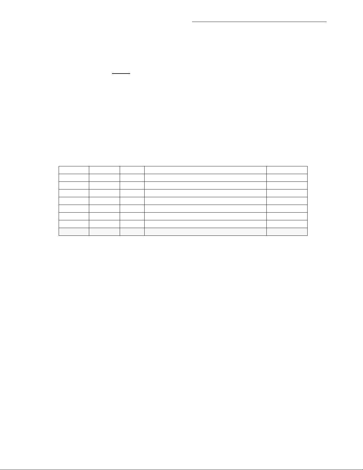
reserved for the addresses of system configuration registers (see Table 2-1). These registers have seven addresses within $0F0-$0FF. The MC68LC302 uses one of the IMP 32-bit
reserved spaces for 3 registers added for the MC68LC302. These registers are used to control the PLL, clock generation and low power modes. See 2.4 Clock Generation and Low
Power Control.
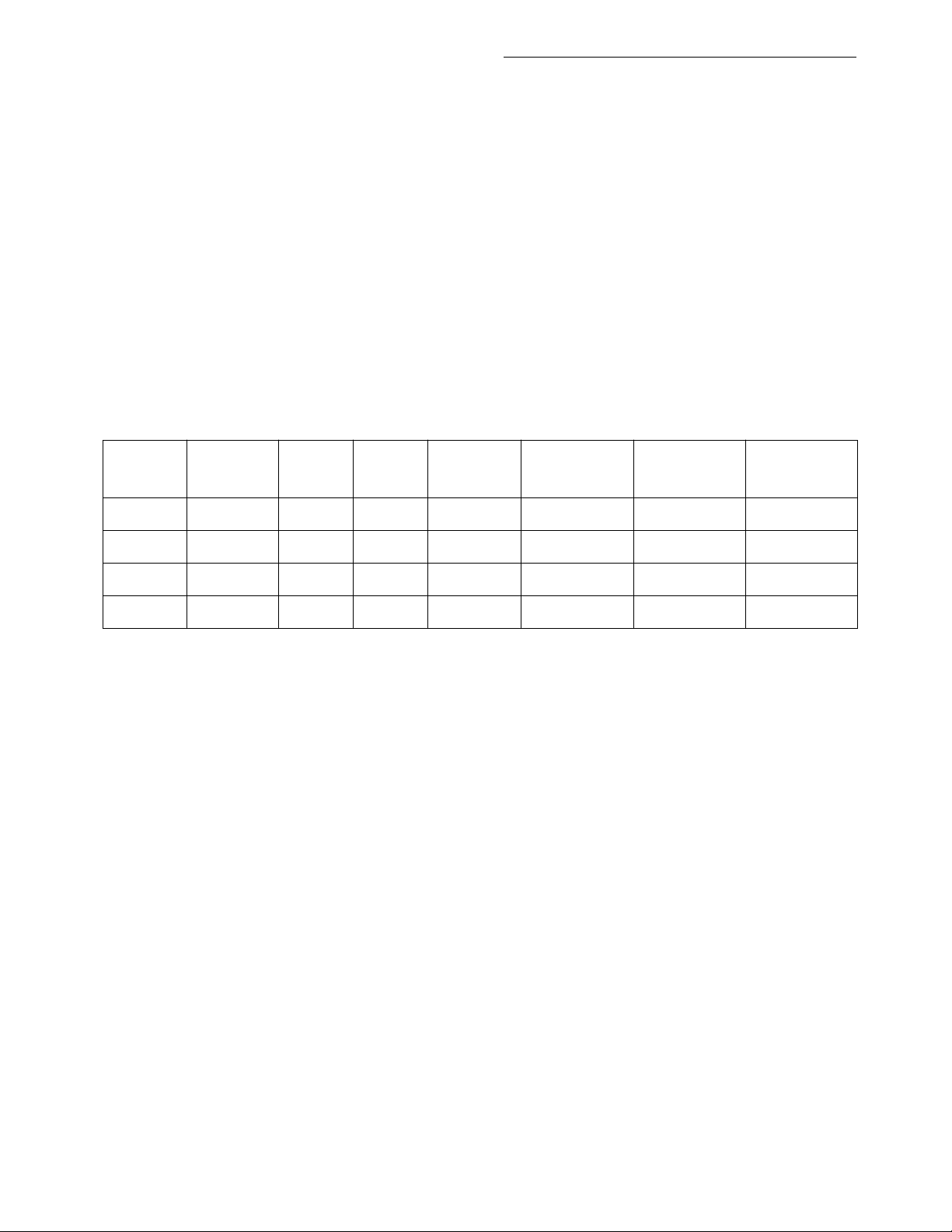
Table 2-1. System Configuration Registers
Address Name Width Description Reset Value
$0F0 PITR 16 Periodic Interrupt Timer Register 0000
$0F2 BAR 16 Base Address Register BFFF
$0F4 SCR 24 System Control Register 0000 0F
$0F7 IWUCR 8 IMP Wake-Up Control Register 00
$0F8 IPLCR 16 IMP PLL Control Register
$0FA IOMCR 8 IMP Operations Mode Control Register 00
$0FB IPDR 8 IMP Power Down Register 00
$0FC RES 32 Reserved
2.4 CLOCK GENERATION AND LOW POWER CONTROL
The MC68LC302 includes a clock circuit that consists of crystal oscillator drive circuit capable of driving either an external crystal or accepting an oscillator clock, a PLL clock synthesizer capable of multiplying a low frequency clock or crystal such as a 32-kHz watch crystal
up to the maximum clock rate of each processor, and a low power divider which allows
dynamic gear down and gear up of the system clock for each processor on the fly.
• On-Chip Clock Synthesizers (with output system clocks)
—Oscillator Drive Circuits and Pins
—PLL Clock Synthesizer Circuits with Low Power Output Clock Divider Block.
• Low Power Control Of IMP
—Slow-Go Modes using PLL Clock Divider Blocks
—Varied Low Power STOP Modes for Optimizing Wake-Up Time to Low Power
Mode Power Consumption: Stand-By, Doze and STOP.
2.4.1 PLL and Oscillator Changes to IMP
The oscillator that was on the MC68302 has been replaced by the new clock synthesizer
described in this section.The registers related to the oscillator have been either removed or
MOTOROLA
MC68LC302 REFERENCE MANUAL
2-5
Page 19

Configuration, Clocking, Low Power Modes, and Internal Memory Map
changed according to the description below. Several control bits are still available but have
new locations.
The low power modes on the MC68302 have changed completely and will be discussed
later in 2.4.4.1 IMP Low Power Modes.
2.4.1.1 CLOCK CONTROL REGISTER. The clock control register address $FA is not
implemented on the MC68LC302. This register location has been reassigned to the IOMCR
and ICKCR registers. The clock control register bits have been reassigned as follows:
CLKO Drive Options (CLKOMOD1–2)
These bits are now in the IMP clock control register (IPLCR) on the MC68LC302, see
2.4.3.4.2 IMP PLL and Clock Control Register (IPLCR).
Three-State TCLK1 (TSTCLK1)
This bit is now in the DISC register on the MC68LC302, see 4.3.2 Disable SCC1 Serial
Clocks Out (DISC).
Three-State RCLK1 (TSRCLK1)
This bit is now in the DISC register on the MC68LC302, see 4.3.2 Disable SCC1 Serial
Clocks Out (DISC).
Disable BRG1 (DISBRG1)
This bit has been removed since the BRG1 pin was removed.
2.4.2 MC68LC302 System Clock Generation
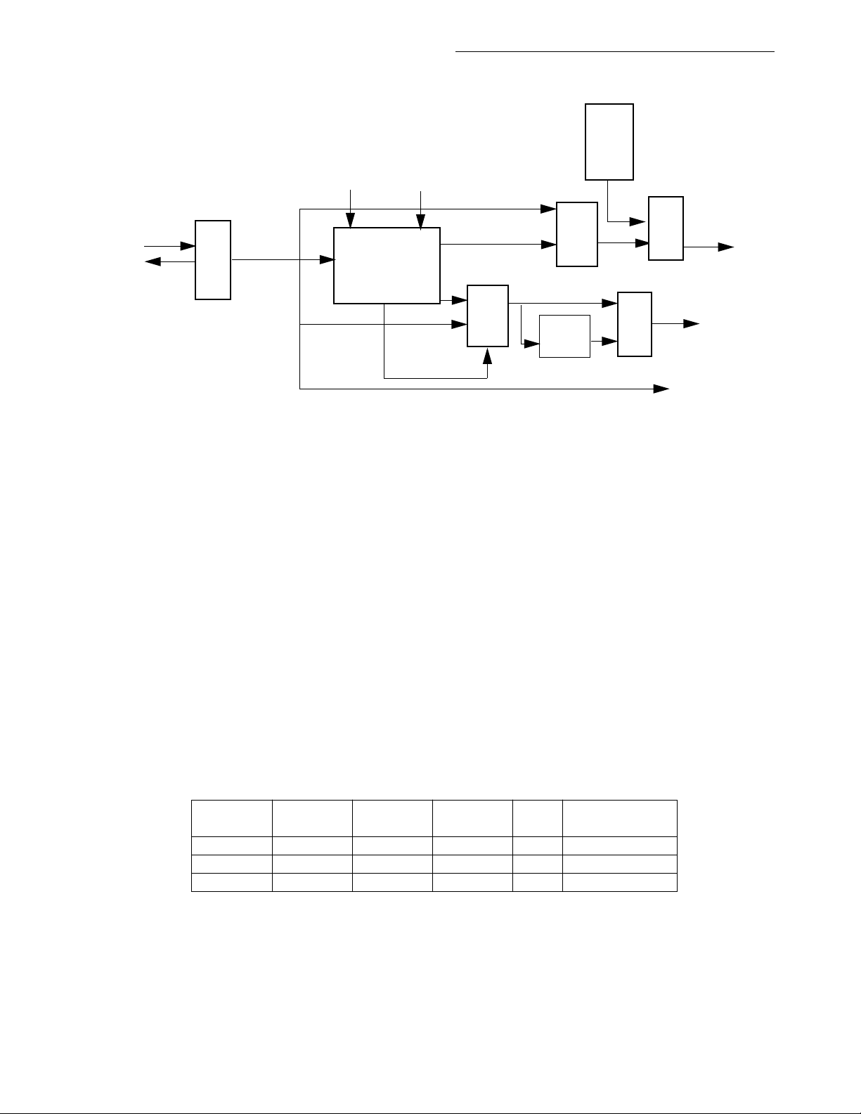
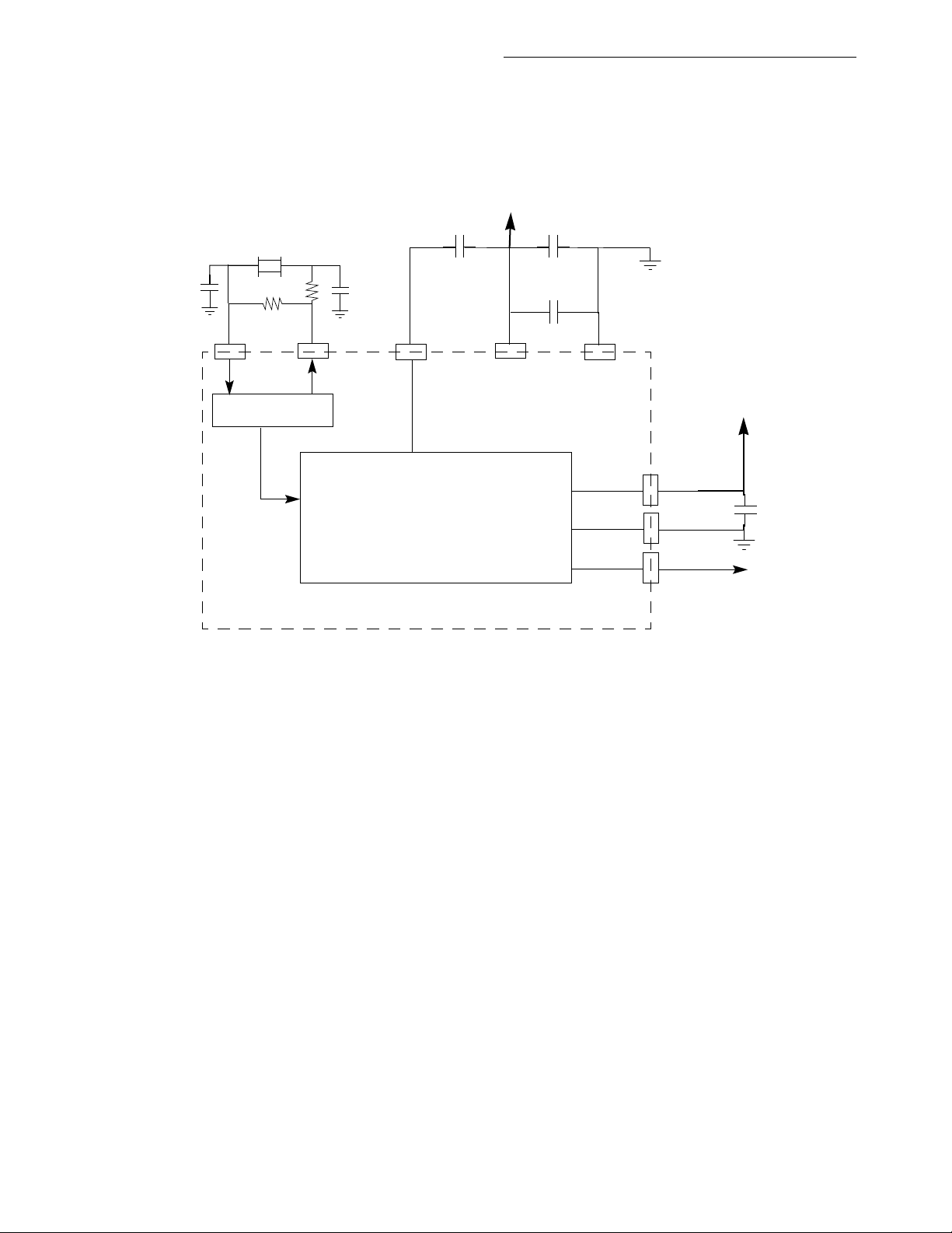
Figure 2-3, the MC68LC302 system clock schematic, shows the IMP clock synthesizer. The
block includes an on-chip oscillator, a clock synthesizer, and a low-power divider, which
allows a comprehensive set of options for generating the system clock. The choices offer
many opportunities to save power and system cost, without sacrificing flexibility and control.
In addition to performing frequency multiplication, the PLL block can also provide EXTAL to
CLKO skew elimination, and dynamic low power divides of the output PLL system clock.
Clock source and default settings are determined during the reset of the IMP. The
MC68LC302 decodes the MODCLK and VCCSYN pins and the value of these pins determines the initial clocking for the part. Further changes to the clocking scheme can be made
by software. After reset, the 68000 core can control the IMP clocking through the following
registers:
1. IMP Operation Mode Control Register, IOMCR (2.4.4.1.6 IMP Operation Mode Control
Register (IOMCR)).
2. IMP PLL and Clock Control Register, IPLCR (2.4.3.4 Frequency Multiplication).
3. IMP Interrupt Wake-Up Control Register, IWUCR (2.4.4.2.4 IMP Wake-Up Control
Register (IWUCR)).
4. Periodic Interrupt Timer Register, PITR (See Section 3 System Integration Block
).
(SIB)
2-6
MC68LC302 REFERENCE MANUAL
MOTOROLA
Page 20
Configuration, Clocking, Low Power Modes, and Internal Memory Map
MULTIPLICATION FACTOR
(MF11–MF0)
Fast
Wake
Up
DIVIDE FACTOR
(DF3–DF0)
RINGO
EXTAL
PIN
XTAL
PIN
IMP
OSC.
CLKIN
IMP PLL
En
CLK OUT
VCO OUT
MUX
MUX
DIVIDE
MUX
IMP SYSTEM
CLOCK
MUX
(0 – Max
Operating Freq)
BRG
CLOCK
BY 2
CLOCK
PIT
Figure 2-2. MC68LC302 PLL Clock Generation Schematic
2.4.2.1 DEFAULT SYSTEM CLOCK GENERATION. During the assertion of hardware
reset, the value of the MODCLK and VCCSYN input pins determine the initial PLL settings
according to Table 2-2. After the deassertion of reset, these pins are ignored.
The MODCLK and VCCSYN pins control the IMP clock selection at hardware reset. The IMP
PLL can be enabled or disabled at reset only and the multiplication factor preset to support
different industry standard crystals. After reset, the multiplication factor can be changed in
the IPLCR register, and the IMP PLL divide factor can be set in the IOMCR register.
MOTOROLA
NOTE
The IMP input frequency ranges are limited to between 25 kHz
and the maximum operating frequency, and the PLL output frequency range before the low power divider is limited to between
10 MHz and the maximum system clock frequency (25 MHz).
Table 2-2. Default System Clock Generation
CSelect
0 0X 25 MHz Disabled x IMP EXTAL
0 10 4.192 MHz Enabled 4 IMP EXTALx4
0 11 32.768 kHz Enabled 401 IMP EXTALx401
Note:
By loading the IPLCR register the user can change the multiplication factor of the PLL
after RESET.
By loading the IOMCR register, the user can change the power saving divide factor of
the IMP PLL.
VCCSYN
MODCLK
Example IMP
EXTAL Freq.
IMP PLL
IMP
MF+1
MC68LC302 REFERENCE MANUAL
IMP System Clock
2-7
Page 21
.
Configuration, Clocking, Low Power Modes, and Internal Memory Map
NOTE
It is not possible to start the system with PLL disabled and then
enable the PLL with software programming.
2.4.3 IMP System Clock Generation
2.4.3.1 SYSTEM CLOCK CONFIGURATION. The IMP has an on-chip oscillator and
phased locked loop (Figure 2-2). These features provide flexible ways to save power and
reduce system cost. The operation of the clock generation circuitry is determined by the following registers.
The IMP Operation Mode Control Register, IOMCR in 2.4.4.1.6 IMP Operation Mode Control Register (IOMCR).
The IMP PLL and Clock Control Register, IPLCR in A 32.768-kHz watch crystal provides
an inexpensive reference, but the EXTAL reference crystal frequency can be any frequency
from 25 kHz to 6.0 MHz. Additionally, the system clock frequency can be driven directly onto
the EXTAL pin. In this case, the EXTAL frequency should be the exact system frequency
desired (0 to Maximum Operating Frequency) and the XTAL pin should be left floating. Figure 2-4 shows all the external connections required for the on-chip oscillator (as well as the
PLL, VCC, and GND connection
PIT
CLOCK
EXTAL
PIN
XTAL
PIN
IMP
OSC.
CLKIN
DIVIDE
BY 2
* MOF is Maximum Operating Frequency
IMP SYSTEM CLOCK
(0 – MOF*)
BRG
CLOCK
MUX
Figure 2-3. IMP System Clocks Schematic - PLL Disabled
Figure 2-2 shows the IMP system clocks schematic with the IMP PLL enabled. Figure 2-3
shows the IMP system clocks schematic with the IMP PLL disabled.
The clock generation features of the IMP are discussed in the following paragraphs.
2.4.3.2 ON-CHIP OSCILLATOR. A 32.768-kHz watch crystal provides an inexpensive ref-
erence, but the EXTAL reference crystal frequency can be any frequency from 25 kHz to 6.0
2-8
MC68LC302 REFERENCE MANUAL
MOTOROLA
Page 22
Configuration, Clocking, Low Power Modes, and Internal Memory Map
MHz. Additionally, the system clock frequency can be driven directly onto the EXTAL pin. In
this case, the EXTAL frequency should be the exact system frequency desired (0 to Maximum Operating Frequency) and the XTAL pin should be left floating. Figure 2-4 shows all
the external connections required for the on-chip oscillator (as well as the PLL, VCC, and
GND connection
VCC
~390pf x MF
0.1µF
CRYSTAL
20pf
EXTAL
330K
20M
CRYSTAL
OSCILLATOR
20pf
XTAL
XFC
CLOCK GENERATION
VCCSYN
0.01µF
GNDSYN
ICLVCC
ICLGND
CLKO
VCC
0.1µF
Figure 2-4. PLL External Components
2.4.3.3 PHASE-LOCKED LOOP (PLL). The IMP PLL’s main function is frequency multipli-
cation. The phase-locked loop takes the CLKIN frequency and outputs a high-frequency
source used to derive the general system frequency of the IMP. The IMP PLL is comprised
of a phase detector, loop filter, voltage-controlled oscillator (VCO), and multiplication block.
2.4.3.4 FREQUENCY MULTIPLICATION. The IMP PLL can multiply the CLKIN input fre-
quency by any integer between 1 and 4096. The multiplication factor may be changed to the
desired value by writing the MF11–MF0 bits in the IPLCR. When the IMP PLL multiplier is
modified in software, the IMP PLL will lose lock, and the clocking of the IMP will stop until
lock is regained (worst case is 2500 EXTAL clocks). If an alteration in the system clock rate
is desired without losing IMP PLL lock, the value in the low-power clock divider can be to
modified to lower the system clock rate dynamically. The low power clock divider bits are
located in the IOMCR register.
NOTE
If IMP PLL is enabled, the multiplication value must be large
enough to result in the VCO clock being greater than 10 MHz.
MOTOROLA
MC68LC302 REFERENCE MANUAL
2-9
Page 23

Configuration, Clocking, Low Power Modes, and Internal Memory Map
2.4.3.4.1 Low Power PLL Clock Divider. The output of the IMP VCO is sent to a low
power divider block. The clock divider can divide the output frequency of the VCO before it
generates the system clock. The clock for the baud rate generators (BRGs) bypasses this
clock divider.
The purpose of the clock divider is to allow the user to reduce and restore the operating frequency of the IMP without losing the IMP’s PLL lock. Using the clock divider, the user can
still obtain full IMP operation, but at a slower frequency. The BRG is not affected by the low
power divider circuitry so previous BRG divider settings will not have to be changed when
the divide factors are changed.
When the PLL low power divider bits (DF0–3) are programmed to a non-zero value, the IMP
is in SLOW_GO mode. The selection and speed of the SLOW_GO mode may be changed
at any time, with changes occurring immediately.
NOTE
The IMP low power clock divider is active only if the IMP PLL is
active.
The low-power divider block is controlled in the IOMCR. The default state of the low-power
divider is to divide all clocks by 1.
If the low-power divider block is not used and the user is concerned that errant software
could accidentally write the IOMCR, the user may set a write protection bit in IOMCR to prevent further writes to the register.
2.4.3.4.2 IMP PLL and Clock Control Register (IPLCR). IPLCR is a 16-bit read/write reg-
ister used to control the IMP’s PLL, multiplication factor and CLKO drive strength. This register is mapped in the 68000 bus space at address $0F8. If the 68000 bus is set to 8 bits
(BUSW grounded at reset), during 8-bit accesses, changes to the IPLCR will take effect in
the IMP PLL after loading the high byte of IPLCR (the low byte is written first). The WP bit
in IPLCR is used as a protect mechanism to prevent erroneous writing. When this bit is set
further accesses to the IPLCR will be blocked.
IMP PLL and Clock Control Register (IPLCR) $0F8
15 14 13 12 11 10 9 8
IPLWP CLKOMOD0–1 PEN MF11 MF10 MF9 MF8
RESET
0 0 0 VCCSYN 0 0 0 VCCSYN/MODCLK
76543210
MF7 MF6 MF5 MF4 MF3 MF2 MF1 MF0
RESET
VCCSYN/MODCLK1
0 0 VCCSYN/MODCLK 0 0 MODCLK MODCLK
Read/Write
2-10
MC68LC302 REFERENCE MANUAL
MOTOROLA
Page 24

Configuration, Clocking, Low Power Modes, and Internal Memory Map
MF 11–0—Multiplication Factor
These bits define the multiplication factor that will be applied to the IMP PLL input frequency. The multiplication factor can be any integer from 1 to 4096. The system frequency is
((MF bits + 1) x EXTAL). The multiplication factor must be chosen to ensure that the resulting VCO output frequency will be in the range from 10 MHz to the maximum allowed
clock input frequency (e.g. 20 MHz for a 20 MHz IMP).
The value 000 results in a multiplier value of 1. The value $FFF results in a multiplier value
of 4096.
Any time a new value is written into the MF11–MF0 bits, the IMP PLL will lose the lock
condition, and after a delay of 2500 EXTAL clocks, will relock. When the IMP PLL loses
its lock condition, all the clocks that are generated by the IMP PLL are disabled. After
hardware reset, the MF11–MF0 bits default to either 0, 3 or 400 ($190 hex) depending on
the MODCLK and VCCSYN pins (giving a multiplication factor of 1, 4 or 401). If the multiplication factor is 401, then a standard 32.768 kHz crystal generates an initial general
system clock of 13.14 MHz. If the multiplication factor is 4, then a standard 4.192 MHz
crystal generates an initial general system clock of 16.768 MHz. The user would then write
the MF bits or adjust the output frequency to the desired frequency.
NOTE
Since the clock source for the periodic interrupt timer is CLKIN
(see Figure 2-2), the PIT timer is not disturbed when the IMP
PLL is in the process of acquiring lock.
PEN—PLL Enable Bit
The PEN bit indicates whether the IMP PLL is operating. This bit is written by the
MC68LC302 based on the value of VCCSYN during reset. When the IMP PLL is disabled,
the VCO is not operating in order to minimize power consumption. During hardware reset
this bit is set if the VCCSYN pin specifies that the IMP PLL is enabled. The only way to
clear PEN is to hold the VCCSYN pin low during a hardware reset.
0 = The IMP PLL is disabled. Clocks are derived directly from the EXTAL pin.
1 = The IMP PLL is enabled. Clocks are derived from the CLKOUT output of the PLL.
CLKODM0–1—CLKO Drive Mode 0–1
These bits control the output buffer strength of the CLKO pin. Those bits can be dynamically changed without generating spikes on the CLKO pin. Disabling CLKO will save power and reduce noise.
00 = Clock Out Enabled, Full-Strength Output Buffer.
01 = Clock Out Enabled, 2/3-Strength Output Buffer
10 = Clock Out Enabled, 1/3-Strength Output Buffer
11 = Clock Out Disabled (CLKO is driven high by internal pullup)
MOTOROLA
NOTE
These IMP bits are in a different address location than in the
MC68302, where they are located at address $FA (bits 15, 14).
MC68LC302 REFERENCE MANUAL
2-11
Page 25

µ
Configuration, Clocking, Low Power Modes, and Internal Memory Map
IPLWP—IMP PLL Control Write Protect Bit
This bit prevents accidental writing into the IPLCR. After reset, this bit defaults to zero to
enable writing. Setting this bit prevents further writing (excluding the first write that sets
this bit).
2.4.3.5 IMP INTERNAL CLOCK SIGNALS. The following paragraphs describe the IMP
internal clock signals.
2.4.3.5.1 IMP System Clock. The IMP system clock is supplied to all modules on the IMP
(with the exception of the BRG clocks which are connected directly to the VCO output with
the PLL enabled). The IMP can be programmed to operate with or without IMP PLL. If IMP
PLL is active, the system clock will be driven by PLL clock divider output. If IMP PLL is not
active, the system clock will be driven by the PLL input clock (CLKIN).
2.4.3.5.2 BRG Clock. The clock to the BRGs can be supplied from the IMP PLL input
(CLKIN) when the IMP PLL is disabled, or from the IMP PLL VCO output (when the PLL is
enabled). The BRG prescaler input clock may be optionally programmed to be divided by 2
to allow very low baud rates to be generated from the system clock by setting the BCD bit
in the IOMCR.
2.4.3.5.3 PIT Clock. CLKIN is supplied to the periodic interrupt timer (PIT) submodule
which allows the PIT clock to run independently of the system clock (refer to Figure 2-2 and
Section 3 System Integration Block (SIB)).
2.4.3.6 IMP PLL PINS. The following pins are dedicated to the IMP PLL operation.
2.4.3.6.1 VCCSYN. This pin is the V
dedicated to the analog IMP PLL circuits. The volt-
CC
age should be well regulated, and the pin should be provided with an extremely low-impedance path to the V
to GNDSYN by a 0.1-
power rail if the PLL is to be enabled. VCCSYN should be bypassed
CC
F capacitor located as close as possible to the chip package.
VCCSYN should be tied to ground if the PLL is to be disabled.
2.4.3.6.2 GNDSYN. This pin is the GND dedicated to the analog IMP PLL circuits. The pin
should be provided with an extremely low-impedance path to ground. GDNSYN should be
bypassed to VCCSYN by a 0.1
µF capacitor located as close as possible to the chip package. The user should also bypass GNDSYN to VCCSYN with a 0.01 µF capacitor as close
as possible to the chip package.
2.4.3.6.3 XFC. This pin connects to the off-chip capacitor for the PLL filter. One terminal of
the capacitor is connected to XFC; the other terminal is connected to IQVCC.
2.4.3.6.4 MODCLK. MODCLK specifies what the initial VCO frequency is after a hardware
reset if VCCSYN is tied high. During the assertion of RESET, the value of the VCCSYN and
MODCLK input pins causes the PEN bit and the MF11–0 bits of the IMP PLL and Clock Control Register (IPLCR) $0F8 to be appropriately written.VCCSYN and MODCLK also determines if the oscillator’s prescaler is used. After RESET is negated, the MODCLK pins is
ignored and becomes PA12. Table 2-2 shows the combinations of VCCSYN and MODCLK
pins with the corresponding default settings.
2-12
MC68LC302 REFERENCE MANUAL
MOTOROLA
Page 26
Configuration, Clocking, Low Power Modes, and Internal Memory Map
2.4.4 IMP Power Management
The IMP portion of the MC68LC302 has several low power modes from which to choose.
2.4.4.1 IMP LOW POWER MODES. The MC68LC302 provides a number of low power
modes for the IMP section. Each of the operation modes has different current consumption,
wake-up time, and functionality characteristics. The state of the IMP’s 68000 data and
address bus lines can be either driven high, low or high impedance during low power stop
mode by programming the low power drive control register (LPDCR).
NOTE
For lowest current consumption, the SCCs and BRGs should be
disabled before entering the low power modes. Current consumption for all operating modes is specified in Section 6 Electrical Characteristics.
Table 2-3. IMP Low Power Modes - IMP PLL Enabled
Operation
Mode
STOP Not Active Not active Not active
DOZE Active Not active Not active
STAND_BY Active
SLOW_GO/
NORMAL
Oscillator PLL IMP Clock
Active
Active (if
enabled
Active (if
enabled)
Not active
Wake_Up
(Osc. Clock
Cycles)
70000 osc.
clocks
2500 osc
clocks
2–5 system
clock cycles
Active
Current
Consumption
(Approximate)
<0.1mA
About 500uA
About 5mA
Low, depends on
CLK freq.
Method of Entry/
LPM bits
Stop instruction/
LPM1–0=11
Stop instruction/
LPM1–0=10
Stop instruction/
LPM1–0=01
Write to DF3–0 Full
Functionality
Partial (BRG
clock is active)
IMP
No
No
2.4.4.1.1 STOP Mode. In STOP mode, all parts of IMP are inactive and the current consumption is less than 0.1mA. Both the crystal oscillator and the IMP PLL are shut down.
Because both the oscillator and the PLL must start up, the wake-up time takes 70000
EXTAL clocks (for example, 70000 cycles of 32.768 kHz crystal will take about 2.2 seconds).
The STOP mode is entered by executing the STOP instruction with the LPM0–1 bits in the
IOMCR register set to 11. Refer to 2.4.4.2.2 Entering the STOP/ DOZE/ STAND_BY Mode
for an example instruction sequence for use with the STOP instruction.
2.4.4.1.2 DOZE Mode. In DOZE mode, the oscillator is active in the IMP but the IMP PLL is
shut down. The current consumption depends on the frequency of the external crystal but is
on the order of 500 µA. In DOZE mode, the IMP is shut down. The wake-up time is 2500
cycles of the external crystal (for example, 2500 cycles of 32.768 kHz crystal will take about
80 milliseconds.). Doze mode has faster wake-up time than the STOP mode, at the price of
higher current consumption.
The DOZE mode is entered by executing the STOP instruction with the LPM1–0 bits in the
IOMCR register set to 10. Refer to 2.4.4.2.2 Entering the STOP/ DOZE/ STAND_BY Mode
for an example instruction sequence for use with the STOP instruction.
2.4.4.1.3 STAND_BY Mode. In STAND_BY mode, the oscillator is active, and the IMP PLL,
if enabled, is active but the IMP clock is not active and the IMP is shut down. Current con-
MOTOROLA MC68LC302 REFERENCE MANUAL 2-13
Page 27

Configuration, Clocking, Low Power Modes, and Internal Memory Map
sumption in STAND-BY mode is less than less than 5mA. The wake up time is a few IMP
system clock cycles.
The STAND_BY mode is entered by executing the STOP instruction with the LPM1–0 bits
in the IOMCR register set to 01. Refer to 2.4.4.2.2 Entering the STOP/ DOZE/ STAND_BY
Mode for an example instruction sequence for use with the STOP instruction.
2.4.4.1.4 SLOW_GO Mode. In the SLOW-GO mode, the IMP is fully operational but the
IMP PLL divider has been programmed with a value that is dividing the IMP PLL VCO output
to the system clock in order to save power. The PLL output divider can only be used with
the IMP PLL enabled. The divider value is programmed in the DF3–0 bits in the IOMCR. The
0
clock may be divided by a power of 2 (2
– 215). No functionality is lost in SLOW-GO mode.
2.4.4.1.5 NORMAL Mode. In NORMAL mode the IMP part is fully operational and the system clock from the PLL is not being divided down.
2.4.4.1.6 IMP Operation Mode Control Register (IOMCR). IOMCR is a 8-bit read/ write
register used to control the operation modes of the IMP. The WP bit in IOMCR is used as a
protect mechanism to prevent erroneous writing of IOMCR.
IOMCR $0FA
76543210
IOMWP DF3 DF2 DF1 DF0 BCD LPM1 LPM0
RESET :
0
0000000
Read/Write
IOMWP—IMP Operation Mode Control Write Protect Bit
This bit prevents accidental writing into the IOMCR. After reset, this bit defaults to zero to
enable writing. Setting this bit prevents further writing (excluding the first write that sets
this bit).
DF 3–0—Divide Factor
The Divide Factor Bits define the divide factor of the low power divider of the PLL. These
0
bits specify a divide range between 2
and 215. Changing the value of these bits will not
cause a loss of lock condition to the IMP PLL.
BCD—BRG Clock Divide Control
This bit controls whether the divide-by-two block shown in Figure 2-2 is enabled.
0 = The BRG clock is divided by 1.
1 = The BRG clock is divided by 2.
2-14 MC68LC302 REFERENCE MANUAL MOTOROLA
Page 28

Configuration, Clocking, Low Power Modes, and Internal Memory Map
LPM—Low Power Modes
When the 68000 core executes the STOP instruction, the IMP will enter the specified
mode.
LPM1–0:
00 = Normal - the IMP PLL and clock oscillator will continue to operate normally.
01 = Stand_by Mode
10 = DOZE Mode
11 = Stop Mode
2.4.4.1.7 Low Power Drive Control Register (LPDCR). This register controls the state of
the IMP’s 68000 address and data buses during the Standby, Doze, and Stop modes. By
programming this register it is possible to minimize power consumption due to external pullups or pull downs, or floating inputs.
LPDCR BAR+$82A
76543210
LPAL LPDL LPDEN
RESET :
0
0000000
Read/Write
LPDEN—Low Power Drive Enable
0 - The IMP 68000 data and address buses will be high impedance.
1 - The IMP 68000 data and address buses to be driven according to the LPDL bit.
LPDL—Low Power Drive Data Low
0 - The data bus will be driven high when the LPDEN bit is set.
1 - The data bus will be driven low when the LPDEN bit is set.
LPAL-Low Power Drive Address Low
0 - The address bus will be driven high when the LPDEN bit is set.
1 - The address bus will be driven low when the LPDEN bit is set.
2.4.4.1.8 IMP Power Down Register (IPWRD). The IPWRD is a 8-bit read/ write register
located at $0FB that is used to control the low power operation of the IMP. This register must
be written with the same operand as the STOP instruction that follows. This tells the hardware what level of interrupt (and above) will stop the MC68LC302 from entering low power
if it occurs while the clocks are being stopped.
2.4.4.1.9 Default Operation Modes, See 2.4.2.1 Default System Clock Generation.
2.4.4.2 LOW POWER SUPPORT. The following sections describe how to enter the various
low power modes.
2.4.4.2.1 Enter the SLOW_GO mode. When the required IMP performance can be
achieved with a lower clock rate, the user can reduce power consumption by dividing IMP
MOTOROLA MC68LC302 REFERENCE MANUAL 2-15
Page 29

Configuration, Clocking, Low Power Modes, and Internal Memory Map
PLL output clock that provides the IMP system clock. Switching between the NORMAL and
SLOW_GO modes is achieved by changing the DF3–0 field in the IOMCR register to a nonzero value. The IMP PLL will not lose lock when the DF3–0 field in the IOMCR register is
changed.
2.4.4.2.2 Entering the STOP/ DOZE/ STAND_BY Mode. Entering the STOP/ DOZE/
STAND_BY mode is achieved by the 68000 core executing the following code:
nop
move.b *+6(PC),$000000FB ;copy STOP operand high byte to addr 000000fb
stop #$xxxx ;xxxx -> SR
nop
This code is position independent. The core must be in the supervisor state to execute the
STOP instruction, therefore the write to $000000FB must be done in the supervisor state
(function code 5, supervisor data). The core trace exception should be disabled, otherwise
the low power control will not enter the STOP mode.
To guarantee supervisor state and trace exceptions disabled, this code should be part of a
TRAP routine. Upon entering the trap routine, examine the stacked status register. If it indicates the supervisor state, then execute this code to enter STOP mode. If not supervisor,
do NOT execute this code (could perform some application-specific error):
TRAP_x btst.b #5,(SP) ; supervisor?
beq.s NO_STOP
nop ; flush execution, bus pipes
move.b *+6(PC),$000000FB ;copy STOP operand high byte to addr 000000fb
stop #$xxxx ; xxxx -> SR
nop
rte
NO_STOP ... ; error routine?
NOTE
The RI/PB9, DTE/PB10, and periodic interrupt timer timeout in-
terrupts conditions will generate level 4 interrupts. The user
should set the 68000 interrupt mask register to the appropriate
level before executing this code.
IMP’s low power control logic will:
1. Detect the write cycle.
2. Check if bit 5 = 1 (supervisor space) (if it is 0, the low power request will be ignored).
3. Sample the interrupt mask bits (bits 0–2). If during this process of stopping the clocks
2-16 MC68LC302 REFERENCE MANUAL MOTOROLA
Page 30

Configuration, Clocking, Low Power Modes, and Internal Memory Map
an interrupt of higher level than the mask is asserted to the core, this process will
abort.
4. Wait for 16 clocks to guarantee the execution of the STOP command by the core. BG
and BGACK
will reset the 16-clock counter and it will restart its count.
5. Assert bus request signal to the core.
6. Wait for Bus Grant from the core
7. Force the IMP to the selected power-down mode, as defined in Table 2-3.
2.4.4.2.3 IMP Wake-Up from Low Power STOP Modes. The IMP can wake up from
STOP/DOZE/STAND_BY mode to NORMAL/SLOW_GO mode in response to inputs from
the following sources:
1. Asserting both RESET
and HALT (hard reset) pins.
2. Asserting (high to low transition) either PB9 or PB10 pins (if these interrupts are enabled).
3. A timeout of the periodic interrupt timer (if the PIT interrupt is enabled).
When one of these events occur (and the corresponding event bit is set), the IMP low power
controller will asynchronously restart the IMP clocks. Then IMP low power control logic will
release the 68000 bus and the IMP will return to normal operation. If one of the above wakeup events occurs during the execution of the STOP command, the low power control logic
will abort the power down sequence and return to normal operation.
NOTE
The RI/PB9, DTE/PB10, and periodic interrupt timer timeout interrupts conditions will generate level 4 interrupts.The user
should also set the 68000 interrupt mask in the status register
(SR) to the appropriate level before executing the STOP command to ensure that the IMP will wake up to the desired events.
2.4.4.2.4 IMP Wake-Up Control Register (IWUCR). The IWUCR contains control for the
wake-up options. This register can be read and written by the 68000 core.
IWUCR $0F7
7 6 5 4 3 2 1 0
0 PITE PB10E PB9Ev 0 PITEn PB10En PB9En
RESET:
0
0 0 0 0 0 0 0
Read/Write
PB9Ev—PB9 Event
This bit will be set to one when there is a high to low transition on the PB9 pin. When
PB9En is set and PB9Ev is set, the IMP will wake-up from the selected power down state,
and a PB9 Interrupt will be generated. The IMP cannot enter the power-down mode if
MOTOROLA MC68LC302 REFERENCE MANUAL 2-17
Page 31

Configuration, Clocking, Low Power Modes, and Internal Memory Map
PB9Ev and PB9En are both set to one. PB9Ev is cleared by writing a one (writing a zero
has no effect).
In modem applications RI
should be connected to the PB9 pin.
PB10Ev—PB10 Event
This bit will be set to one when there is a high to low transition on the PB10 pin. When
PB10En is set and PB10Ev is set, the IMP will wake-up from the selected power down
state, and the PB10 Interrupt will be generated. The IMP cannot enter the power-down
mode when PB10Ev and PB10En are both set to one. PB10Ev is cleared by writing a one
(writing a zero has no effect).
In modem applications the DTE TxD line may be connected to the PB10 pin.
PITEv—PIT Event
This bit will be set to one when there is a time-out on the periodic interrupt timer (PIT).
When PITEn bit is set and a time-out occurs (PITEv is set), the IMP will wake-up from the
selected power down, and a PIT Interrupt will be generated. The IMP cannot enter the
power-down mode if PITEv and PITEn are both set to one. PITEv is cleared by writing a
one (writing a zero has no effect).
PB9En—PB9 Enable
This bit, when set, enables the IMP to wake up from power down mode and generate an
interrupt when the PB9 Event bit becomes set.
PB10En—PB10 Enable
This bit, when set, enables the IMP to wake up from power down mode and generate an
interrupt when the PB10 Event bit becomes set.
PITEn—PIT Enable
This bit, when set, enables the IMP to wake up from power down mode and generate an
interrupt when the PIT event bit becomes set, see 3.7.4 Periodic Interrupt Timer (PIT).
2.4.4.3 FAST WAKE-UP
In a system clocked with a 32-kHz oscillator, the wake-up recovery time from doze and stop
modes may be too long for some applications. In order to shorten this time, an internal ring
oscillator (called Ringo) can clock the chip (the term “real clock” in the following discussion
refers to the clock whose source is the external oscillator or crystal; the PLL can be either
enabled or disabled). One reason for using the fast wake-up is:
• To allow logic to operate in the time frame between the wake-up command and the actual real clock recovery (from the external crystal or oscillator).
NOTE
If the SCCs use the internal clock, or if they use external clock
and the Ringo/external frequency ratio does not comply with the
1 / 2.5 maximum ration specification, then they cannot be enabled until the real clock has resumed operation.
2-18 MC68LC302 REFERENCE MANUAL MOTOROLA
Page 32

Configuration, Clocking, Low Power Modes, and Internal Memory Map
The criteria for enabling Ringo and waking up the CPU (by giving it an interrupt) is: RINGOEN=1 and an unmasked PITEv, PB10Ev, or PB9Ev event occurs (please refer to the
IWUCR register)
The internal ring oscillator is not enabled if the PLL is disabled. A system with the PLL disabled has to have an external oscillator connected in order to shorten the wake-up time.
There are two possible interrupts to the CPU from the Ringo logic:
— Interrupt when Ringo is enabled; the CPU is always interrupted when Ringo starts
oscillating (RINGOEN bit enables both ring oscillator and enables the interrupt to the
CPU). Event bits for this interrupt are all wake-up events.
— Maskable interrupt when the system clock switches to the real clock. The event bit
for this interrupt is in the ring oscillator event register.
The Ringo interrupts can be either at level 1, 6, or 7 according to RICR bits. If the CPU determines that the system needs the real clock, it programs the RECLMODE bits which enables the oscillator and PLL and interrupts if necessary; if it decides that the system can go
back to sleep, it executes the normal power-down sequence which turns off Ringo. Upon
switching to the real clock, the CPU can be interrupted by programming the RICR bits. (Note
that Ringo is turned off either at the end of a power down sequence, or when the PLL has
gained lock). If the RECLMODE bits are programmed to enable the PLL and the oscillator,
after
the user is allowed to enter low power mode
the real clock has resumed. The chip will
not operate correctly if the CPU enters the low power sequence while the PLL is waking up.
Resetting of the RINGOEN bit is allowed only if the system is clocked by the real clock. The
CLKO signal can be disabled by software if the user cannot operate the system at the Ringo
frequency.
2.4.4.3.5 Ring Oscillator Control Register (RINGOCR)
RINGOCR BAR+$81A
76543210
RICR RECLMODE RINGOEN
RESET:
0
0000000
Read/Write
RINGOEN — Ring Oscillator Enable
0 = Ring oscillator is not used
1 = Ring oscillator is enabled
RECLMODE — Real Clock Mode
00 = Do not enable the real clock
01 = Enable the real clock and switch the system clock from Ringo to the real clock
once it is stable
10 = Enable the real clock and generate an interrupt to the CPU after the switch occurs
11 = Reserved
MOTOROLA MC68LC302 REFERENCE MANUAL 2-19
Page 33

Configuration, Clocking, Low Power Modes, and Internal Memory Map
RICR — Ring Oscillator Interrupt Control
00 = Connect Ringo Interrupts to 68k interrupt request level 1
01 = Connect Ringo Interrupts to 68k Interrupt request level 6
10 = Connect Ringo Interrupts to 68k interrupt request level 7
11 = Reserved
2.4.4.3.6 Ring Oscillator Event Register (RINGOEVR).
RINGOEVR BAR+$81B
76543210
RESERVED RECLSEV
RESET:
0
0000000
Read/Write
RECLSEV — Real Clock Switch Event
0 = Event has not occurred
1 = Real clock is now the system clock (This bit is reset by writing 1)
Bits 7-1 — Reserved
2.5 MC68LC302 DUAL PORT RAM
The internal 1152-byte dual-port RAM has 576 bytes of system RAM (see Table 2-4) and
576 bytes of parameter RAM (see Table 2-5).
Table 2-4. System RAM
Address Width Block Description
Base + 000
•
•
•
Base + 23F
Base +240
•
•
•
Base + 3FF
The parameter RAM contains the buffer descriptors for each of the two SCC channels, the
SCP, and the two SMC channels. The memory structures of the three SCC channels are
identical. When any SCC, SCP, or SMC channel buffer descriptors or parameters are not
used, their parameter RAM area can be used for additional memory. For detailed information about the use of the buffer descriptors and protocol parameters in a specific protocol,
see Section 4 Communications Processor (CP). CP. Base + 67E contains the MC68LC302
revision number.
576 Bytes RAM User Data Memory
Reserved
(Not Implemented)
2-20 MC68LC302 REFERENCE MANUAL MOTOROLA
Page 34

Configuration, Clocking, Low Power Modes, and Internal Memory Map
Table 2-5. Parameter RAM
Address Width Block Description
Base + 400
Base + 408
Base + 410
Base + 418
Base + 420
Base + 428
Base + 430
Base + 438
Base + 440
Base + 448
Base + 450
Base + 458
Base + 460
Base + 468
Base + 470
Base + 478
Base + 480
•
•
•
Base + 4BF
Base + 4C0
•
•
Base + 4FF
Base + 500
Base + 508
Base + 510
Base + 518
Base + 520
Base + 528
Base + 530
Base + 538
Base + 540
Base + 548
Base + 550
Base + 558
Base + 560
Base + 568
Base + 570
Base + 578
Base + 580
•
•
•
Base + 5BF
Base + 5C0
•
•
Base + 5FF
Base + 600
•
•
Base + 65F
Base + 660
Base + 666
Base + 668
Base + 66A
Base + 66C
Base + 66E #
Base + 67A
Base + 67C
Base + 67E #
Base + 680
•
•
•
Base + 6BF
Base + 6C0
•
•
Base + 7FF
# Modified by the CP after a CP or system reset.
4 Word
4 Word
4 Word
4 Word
4 Word
4 Word
4 Word
4 Word
4 Word
4 Word
4 Word
4 Word
4 Word
4 Word
4 Word
4 Word
4 Word
4 Word
4 Word
4 Word
4 Word
4 Word
4 Word
4 Word
4 Word
4 Word
4 Word
4 Word
4 Word
4 Word
4 Word
4 Word
48 Words
3 Word
Word
Word
Word
Word
6 Word
Word
Word
Word
SCC1
SCC1
SCC1
SCC1
SCC1
SCC1
SCC1
SCC1
SCC1
SCC1
SCC1
SCC1
SCC1
SCC1
SCC1
SCC1
SCC1
SCC1
SCC2
SCC2
SCC2
SCC2
SCC2
SCC2
SCC2
SCC2
SCC2
SCC2
SCC2
SCC2
SCC2
SCC2
SCC2
SCC2
SCC2
SCC2
SMC
SMC1
SMC1
SMC2
SMC2
SMC1–SMC2
SCP
SCC1–SCC3
CP
Specific Protocol Parameters
(Not Implemented)
Tx BD 6/DRAM Refresh
Tx BD 7/DRAM Refresh
Specific Protocol Parameters
(Not Implemented)
Not Used by CP
(Available to User)
BERR Channel Number
MC68PM302 Revision Number
(Not Implemented)
Rx BD 0
Rx BD 1
Rx BD 2
Rx BD 3
Rx BD 4
Rx BD 5
Rx BD 6
Rx BD 7
Tx BD 0
Tx BD 1
Tx BD 2
Tx BD 3
Tx BD 4
Tx BD 5
Tx BD 6
Tx BD 7
Reserved
Rx BD 0
Rx BD 1
Rx BD 2
Rx BD 3
Rx BD 4
Rx BD 5
Rx BD 6
Rx BD 7
Tx BD 0
Tx BD 1
Tx BD 2
Tx BD 3
Tx BD 4
Tx BD 5
Reserved
Reserved
Rx BD
Tx BD
Rx BD
Tx BD
Internal Use
Rx/Tx BD
Reserved
Reserved
MOTOROLA MC68LC302 REFERENCE MANUAL 2-21
Page 35

Configuration, Clocking, Low Power Modes, and Internal Memory Map
In addition to the internal dual-port RAM, a number of internal registers support the functions
of the various M68000 core peripherals. The internal registers (see Table 2-6) are memorymapped registers offset from the BAR pointer and are located on the internal M68000 bus.
NOTE
All undefined and reserved bits within registers and parameter
RAM values written by the user in a given application should be
written with zero to allow for future enhancements to the device.
2-22 MC68LC302 REFERENCE MANUAL MOTOROLA
Page 36

Configuration, Clocking, Low Power Modes, and Internal Memory Map
2.6 INTERNAL REGISTERS MAP
Table 2-6. Internal Registers Map
Address Name Width Block Description Reset Value
Base + 800 RES 16 IDMA Reserved
Base + 802 CMR 16 IDMA Channel Mode Register 0000 0000
Base + 804 SAPR 32 IDMA Source Address Pointer XXXX XXXX
Base + 808 DAPR 32 IDMA Destination Address Pointer XXXX
Base + 80C BCR 16 IDMA Byte Count Register 00
Base + 80E * CSR 8 IDMA Channel Status Register
Base + 80F RES 8 IDMA Reserved
Base + 810 FCR 8 IDMA Function Code Register XX
Base + 811 RES 8 IDMA Reserved
Base + 812
Base + 814 * IPR 16 Int Cont Interrupt Pending Register 0000
Base + 816 IMR 16 Int Cont Interrupt Mask Register 0000
Base + 818 * ISR 16 Int Cont In-Service Register 0000
Base + 81A RINGOCR 8 Int Cont Ring Oscillator Control Register 00
Base + 81B RINGOEVR 8 Int Cont Ring Oscillator Event Register 00
Base + 81C RES 16 Int Cont Reserved
Base + 81E # PACNT 16 PIO Port A Control Register 0000
Base + 820 # PADDR 16 PIO Port A Data Direction Register 0000
Base + 822 # PADAT 16 PIO Port A Data Register XXXX ##
Base + 824 # PBCNT 16 PIO Port B Control Register 0080
Base + 826 # PBDDR 16 PIO Port B Data Direction Register 0000
Base + 828 # PBDAT 16 PIO Port B Data Register XXXX ##
Base + 82A LPDCR 8 PIO Low Power Drive Control Register 00
Base + 82C BSR 8 CS Bus Switch register 0000
Base + 82E RES 16 CS Reserved
Base + 830 # BR0 16 CS0 Base Register 0 C001
Base + 832 # OR0 16 CS0 Option Register 0 DFFD
Base + 834 # BR1 16 CS1 Base Register 1 C000
Base + 836 # OR1 16 CS1 Option Register 1 DFFD
Base + 838 # BR2 16 CS2 Base Register 2 C000
Base + 83A # OR2 16 CS2 Option Register 2 DFFD
Base + 83C # BR3 16 CS3 Base Register 3 C000
Base + 83E # OR3 16 CS3 Option Register 3 DFFD
Base + 840 TMR1 16 Timer Timer Unit 1 Mode Register 0000
Base + 842 TRR1 16 Timer Timer Unit 1 Reference Register FFFF
Base + 844 TCR1 16 Timer Timer Unit 1 Capture Register 0000
Base + 846 TCN1 16 Timer Timer Unit 1 Counter 0000
Base + 848 RES 8 Timer Reserved
Base + 849 * TER1 8 Timer Timer Unit 1 Event Register 00
Base + 84A WRR 16 WD Watchdog Reference Register FFFF
Base + 84C WCN 16 WD Watchdog Counter 0000
Base + 84E RES 16 Timer Reserved
Base + 850 TMR2 16 Timer Timer Unit 2 Mode Register 0000
Base + 852 TRR2 16 Timer Timer Unit 2 Reference Register FFFF
Base + 854 TCR2 16 Timer Timer Unit 2 Capture Register 0000
Base + 856 TCN2 16 Timer Timer Unit 2 Counter 0000
Base + 858 RES 8 Timer Reserved
#
GIMR 16 Int Cont Global Interrupt Mode Register 0000
MOTOROLA MC68LC302 REFERENCE MANUAL 2-23
Page 37

Configuration, Clocking, Low Power Modes, and Internal Memory Map
Table 2-6. Internal Registers Map
Address Name Width Block Description Reset Value
Base + 859 * TER2 8 Timer Timer Unit 2 Event Register 00
Base + 85A RES 16 Timer Reserved
Base + 85C RES 16 Timer Reserved
Base + 85E RES 16 Timer Reserved
Base + 860 CR 8 CP Command Register 00
Base + 861 Reserved
Base + 87F
Base + 880 RES 16 SCC1 Reserved
Base + 882 SCON1 16 SCC1 SCC1 Configuration Register 0004
Base + 884 SCM1 16 SCC1 SCC1 Mode Register 0000
Base + 886 DSR1 16 SCC1 SCC1 Data Sync. Register 7E7E
Base + 888 * SCCE1 8 SCC1 SCC1 Event Register 00
Base + 889 RES 8 SCC1 Reserved
Base + 88A SCCM1 8 SCC1 SCC1 Mask Register 00
Base + 88B RES 8 SCC1 Reserved
Base + 88C SCCS1 8 SCC1 SCC1 Status Register 00
Base + 88D RES 8 SCC1 Reserved
Base + 88E RES 16 SCC1 Reserved
Base + 890 RES 16 SCC2 Reserved
Base + 892 SCON2 16 SCC2 SCC2 Configuration Register 0004
Base + 894 SCM2 16 SCC2 SCC2 Mode Register 0000
Base + 896 DSR2 16 SCC2 SCC2 Data Sync. Register 7E7E
Base + 898 * SCCE2 16 SCC2 SCC2 Event Register 0000
Base + 899 RES 8 SCC2 Reserved
Base + 89A SCCM2 8 SCC2 SCC2 Mask Register 00
Base + 89B RES 8 SCC2 Reserved
Base + 89C SCCS2 8 SCC2 SCC2 0000
Base + 89D RES 8 SCC2 Reserved
Base + 89E RES 16 SCC2 Reserved
Base + 8A0 Reserved
Base + 8AE
Base + 8B0 SPMODE 16 SCM
Base + 8B2 # SIMASK 16 SI Serial Interface Mask Register FFFF
Base + 8B4 # SIMODE 16 SI Serial Interface Mode Register 0000
Base + 8B6 Reserved
Base +8DA
Base + 8DC # PNDNR 8 PIO Pin IO Data Direction Register 0000
Base + 8DE # PNDAT 8 PIO Pin IO Data Register 0000
Base + 8E0 Reserved
Base +8EC
Base + 8EE # DISC 16 SIB Disable SCC1 Serial Clocks 0000
Base + 8F0 Reserved
Base + FFF
# Reset only upon total system reset. (RESET and HALT assert together), but not on the execution of an
M68000 RESET instruction. See the RESET pin description for details.
## The output latches are undefined at total system reset.
* Event register with special properties.
SCP, SMC Mode and Clock Control
Register
0000
2-24 MC68LC302 REFERENCE MANUAL MOTOROLA
Page 38

SECTION 3
SYSTEM INTEGRATION BLOCK (SIB)
The MC68LC302 contains an extensive SIB that simplifies the job of both the hardware and
software designer. Most of the features are taken from the MC68302 without change, features that have been added are highlighted in
This section will only present the register descriptions for each
block. For more information on the operation of each block,
please refer to the
or have changed will be described in detail.
MC68302 Users’ Manual
bold text.
NOTE
. Items that are new
The SIB includes the following functions:
• IDMA Controller
• Interrupt Controller with Two Modes of Operation
• Parallel Input/Output (I/O) Ports, Some with Interrupt Capability
• Parallel Input/Output Ports on D15-D8 in 8 bit mode
• On-Chip 1152-Byte Dual-Port RAM
• Four Timers Including a Watchdog Timer and
• Four Programmable Chip-Select Lines with Wait-State Generator Logic
•
Glueless Interface to SRAM, EPROM, Flash EPROM, and EEPROM
• System Control
—System Status and Control Logic
—Disable CPU Logic (M68000)
—Bus Arbitration Logic with Low-Interrupt Latency Support (for internal DMA)
—Hardware Watchdog for Monitoring Bus Activity
—DRAM Refresh Controller
—Programmable Bus Width
Periodic Interrupt Timer
• Boot from SCC
3.1 SYSTEM CONTROL
The IMP system functions are configured using the System Control Register (SCR). The following systems are configurated:
• System Status and Control Logic
MOTOROLA
MC68LC302 REFERENCE MANUAL
3-1
Page 39

System Integration Block (SIB)
•AS Control During Read-Modify-Write-Cycles
• Disable CPU (M68000) Logic
• Bus Arbitration Logic with Low-Interrupt Latency Support
(Disable CPU only)
• Hardware Watchdog
• Low-Power (Standby) Modes
• Freeze Control
(Only supported in the PGA package)
3.1.1 System Control Register (SCR)
The SCR is a 32-bit register that consists of system status, control bits, a bus arbiter control
bit, and hardware watchdog control bits. Refer to Figure 3-1 and to the following paragraphs
for a description of each bit in this register. The SCR is a memory-mapped read-write register. The address of this register is fixed at $0F4 in supervisor data space (FC = 5).
$F4
31
Res 0 0 0 I IPA HWT WPV ADC
$F5
23 22 21 20 19 18 17 16
RME ERRE VGE WPVE RMCST EMWS ADCE BCLM
$F6
15 14 13 12 11 10 9 8
FRZW FRZ2 FRZ1 SAM HWDEN HWDCN2–HWDCN0
30 29 28 27 26 25 24
Figure 3-1. System Control Register
Table 3-1. SCR Register Bits
Bit Name
IPA Interrupt Priority Active
HWT Hardware Watchdog Timeout
WPV Write Protect Violation
ADC Address Decode Conflict
RME Ram Microcode Enable
ERRE External RISC Request Enable
VGE Vector Generation Enable
WPVE Write Protect Violation Enable
RMCST Read-Modify-Write Cycle Special Treatment
EMWS External Master Wait State
ADCE Address Decode Conflict Enable
BCLM Bus Clear Mask
FRZW Freeze Watch Dog Timer Enable
FRZ1 Freeze Timer 1 Enable
FRZ2 Freeze Timer 2 Enable
SAM Synchronous Access Mode
HWDEN Hardware Watchdog Enable
HWDCN Hardware Watchdog Count
3-2
MC68LC302 REFERENCE MANUAL
MOTOROLA
Page 40

System Integration Block (SIB)
3.1.2 System Status Bits
Bits 27-24 of the SCR are used to report events recognized by the system control logic. On
recognition of an event, this logic sets the corresponding bit in the SCR. These bits may be
read at any time. A bit is reset by a one and is left unchanged by a zero. More than one bit
may be reset at a time. For more information on these bits, please refer to the
User’ s Manual
.
MC68302
After system reset (simultaneous assertion of RESET
and HALT), these bits are cleared.
IPA—Interrupt Priority Active
This bit is set when the M68000 core has an unmasked interrupt request.
NOTE
If BCLM is set, an interrupt handler will normally clear IPA at the
end of the interrupt routine to allow an alternate bus master to
regain the bus; however, if BCLM is cleared, no additional action
needs to be taken in the interrupt handler.
HWT—Hardware Watchdog Timeout
This bit is set when the hardware watchdog (see 3.1.5 Hardware Watchdog) reaches the
end of its time interval; an internal BERR
is generated following the watchdog timeout,
even if this bit is already set.
WPV—Write Protect Violation
This bit is set when a bus master attempts to write to a location that has RW set to zero
(read only) in its associated base register (BR3–BR0).
ADC—Address Decode Conflict
This bit is set when a conflict has occurred in the chip-select logic because two or more
chip-select lines attempt assertion in the same bus cycle.
3.1.3 System Control Bits
The system control logic uses six control bits in the SCR.
WPVE—Write Protect Violation Enable
0 = an internal BERR
1 = an internal BERR
After system reset, this bit defaults to zero.
WPV will be set regardless of the value of WPVE.
RMCST—RMC Cycle Special Treatment
0 = The locked read-modify-write cycles of the TAS instruction will be identical to the
M68000 (AS
is not asserted when a write protect violation occurs.
is asserted when a write protect violation occurs.
NOTE
and CS will be asserted during the entire cycle). The arbiter will issue
MOTOROLA
MC68LC302 REFERENCE MANUAL
3-3
Page 41

System Integration Block (SIB)
BG, regardless of the M68000 core RMC. If an IMP chip select is used then the
DTACK
generator will insert wait states on the read cycle only.
1 = The IMP uses the internal RMC
of the RMC cycle and reasserts AS
will not be asserted until the end of the write portion. If an IMP chip select is
BG
used, the DTACK
generator will insert wait states on both the read and write portion
of the cycles.
to negate AS and CS at the end of the read portion
and CS at the beginning of the write portion.
The assertion of the internal RMC
by the M68000 core is seen by the arbiter and will prevent the arbiter from issuing bus grants until the completion of M68000-initiated locked
read-modify-write activity. After system reset, this bit defaults to zero.
EMWS—External Master Wait State (EMWS)
(VALID only in Disable CPU Mode)
When EMWS is set and an external master is using the chip-select logic for DTACK generation or is synchronously reading from the internal peripherals (SAM = 1), one additional
wait state will be inserted in every memory cycle to external memory, peripherals, and also, in every cycle to internal memory and peripherals. When EMWS is cleared, all synchronous internal accesses will be with zero wait states and the chip-select logic will
generate DTACK
after the exact programmed number of wait states. The chip-select lines
are asserted slightly earlier for internal master memory cycles than for an external master.
EMWS should be set whenever these timing differences will necessitate an additional wait
state for external masters. After system reset, this bit defaults to zero.
ADCE—Address Decode Conflict Enable
0 = an internal BERR
is not asserted by a conflict in the chip-select logic when two or
more chip-select lines are programmed to overlap the same area.
1 = an internal BERR
is asserted by a conflict in the chip-select logic when two or more
chip-select lines are programmed to overlap the same area.
BCLM—Bus Clear Mask
0 = The arbiter does not use the M68000 core internal IPEND signal to assert the in-
ternal bus clear signals.
1 = The arbiter uses the M68000 core internal IPEND signal to assert the internal bus
clear signals.
SAM—Synchronous Access Mode
(Valid only in Disable CPU Mode)
This bit controls how external masters may access the IMP peripheral area. This bit is not
relevant for applications that do not have external bus masters that access the IMP. In applications such as disable CPU mode, in which the M68000 core is not operating, the user
should note that SAM may be changed by an external master on the first access of the
IMP, but that first write access must be asynchronous with three wait states. (If DTACK
used to terminate bus cycles, this change need not influence hardware.)
0 = Asynchronous accesses. All accesses to the IMP internal RAM and registers (in-
cluding BAR and SCR) by an external master are asynchronous to the IMP clock.
Read and write accesses are with three wait states, and DTACK
is asserted by the
IMP assuming three wait-state accesses. This is the default value.
is
3-4
MC68LC302 REFERENCE MANUAL
MOTOROLA
Page 42

System Integration Block (SIB)
1 = Synchronous accesses. All accesses to the IMP internal RAM and registers (in-
cluding BAR and SCR) must be synchronous to the IMP clock. Synchronous read
accesses may occur with one wait state if EMWS is also set to one.
RME—Ram Microcode Enable
This bit is used to initiate the execution of Communication Processor microcode that
has been loaded into the dual port RAM. See Appendix C in MC68302UM/AD.
VGE—Vector Generation Enable
(Not supported by the MC68LC302)
This bit must be written to zero. Since the MC68LC302 cannot decode an interrupt acknowledge cycle from an external processor without the FC pins, the user should provide
either an autovector signal or a vector back to the host processor during an interrupt acknowledge cycle for the MC68LC302. The user should then read the IPR to determine
which the interrupt source.
3.1.4 Freeze Control
Used to freeze the activity of selected peripherals, FRZ is useful for system debugging purposes (For more information on these bits, please refer to the
FRZ1 — Freeze Timer 1 Enable
0 = Freeze Timer 1 Logic is disabled
1= Freeze Timer 1 Logic is enabled
After system reset this bit defaults to zero.
FRZ2 — Freeze Timer 2 Enable
0 = Freeze Timer 2 Logic is disabled
1= Freeze Timer 2 Logic is enabled
After system reset this bit defaults to zero.
MC68302 Users’ Manual)
:
FRZW — Freeze Watchdog Timer Enable
0 = Freeze Watchdog Timer Logic is disabled
1= Freeze Watchdog Timer Logic is enabled
After system reset this bit defaults to zero.
3.1.5 Hardware Watchdog
The hardware watchdog logic is used to assert an internal BERR and set HWT when a bus
cycle is not terminated by DTACK
elapsed. The hardware watchdog logic uses four bits in the SCR.
HWDEN—Hardware Watchdog Enable
0 = The hardware watchdog is disabled.
1 = The hardware watchdog is enabled.
After system reset, this bit defaults to one to enable the hardware watchdog.
MOTOROLA
and after a programmable number of clock cycles has
MC68LC302 REFERENCE MANUAL
3-5
Page 43

System Integration Block (SIB)
HWDCN–HWDCN0—Hardware Watchdog Count 2–0
000 = an internal BERR
001 = an internal BERR
010 = an internal BERR
011 = an internal BERR
100 = an internal BERR
101 = an internal BERR
110 = an internal BERR
111 = an internal BERR
is asserted after 128 clock cycles (8 µ s, 16-MHz clock)
is asserted after 256 clock cycles (16 µ s, 16-MHz clock)
is asserted after 512 clock cycles (32 µ s, 16-MHz clock)
is asserted after 1K clock cycles (64 µ s, 16-MHz clock)
is asserted after 2K clock cycles (128 µ s, 16-MHz clock)
is asserted after 4K clock cycles (256 µ s, 16-MHz clock)
is asserted after 8K clock cycles (512 µ s, 16-MHz clock)
is asserted after 16K clock cycles (1 ms, 16-MHz clock)
3.2 PROGRAMMABLE DATA BUS SIZE SWITCH
The following procedure allows 68LC302 to be booted in an 8 or 16 bit bus width and then
switched to 16 or 8 bit bus width for future accesses. It does not implement true dynamic
bus sizing, but allows a software reconfiguration of the BUSW pin.
3.2.1 Bus Switch Register (BSR)
BSR Base +$82C
7
0 BSW BSWEN 0 0
0 0 0 0 0
6 5 4 3-0
BWSEN - Bus Width Switch Enable
When this bit is toggled from a zero to a one, the bus width switch mechanism is enabled.
From the point this bit is toggled, the bus width is determined by the BSW bit of this register. If another bus width switch is necessary, this bit must be toggled back to zero and
then one again.
Setting this bit implements a hardware state machine that arbitrates the internal bus away
from the 302 core, changes the BUSW pin internally, and then gives the bus back to the
302 core.
BUSW - Bus Width
This bit determines the bus width after the bus width switch is performed.
0 - Data bus width is 8 bits
1 - Data bus width is 16 bits.
3.2.2 Basic Procedure:
The MC68LC302 is booted in its 8-bit mode by externally connecting the BUSW pin to GND.
It is expected that the MC68LC302 will be executing out of EPROM or flash at this time, and
that no external data memory is available in 8-bit mode.
The MC68LC302 initializes the BAR register to place the 4K block of dual-port RAM and
peripherals in an area that does not overlap the EPROM region. Note that this is part of a
normal 302 initialization sequence. Also note that the CFC bit of the BAR register should
NOT be set -- it must be cleared.
3-6
MC68LC302 REFERENCE MANUAL
MOTOROLA
Page 44

System Integration Block (SIB)
At this time other desired initialization should be completed on the MC68LC302. No bus
masters (IDMA, SDMA, or external) should be enabled.
While in 8-bit mode, the MC68LC302 should initialize the external memory registers that
control the16-bit external memory space. External memory refresh is not enabled at this
time, but all other desired external memory control features should be enabled. Note that
the MC68LC302 does not access the external memory itself yet, only the external memory
control registers.
The 302-based device now copies a special boot code to the user area of the internal dualport RAM of the 302, and then jumps to the start of that code. This code is copied as “data”
to the dual-port RAM.
To summarize, the procedure is then:
• Boot up 302-derivative
• Perform required 8 bit operations
• Write code to the dual port RAM for the bus width change
• Jump to code in the dual port RAM
• When ready to use 16-bit bus width, set the BUSW bit to 1
• Toggle the BWSEN bit from zero to one.
• Allow time for bus arbitration and the instruction pipeline to clear
• Initialize external memory
• Copy boot code from EPROM to external memory space
• Execute code from external memory space
NOTE
The stack which is shared by both codes should be placed in the
dual ported RAM. Copy the stack to dual port RAM after switching to the second RAM and change the stack pointer.
3.3 LOAD BOOT CODE FROM AN SCC
The MC68LC302 provides the capability of downloading program code into SCC1 and
beginning program execution in the dual port RAM. The boot function has two clocking
options: external and internal.
In the first mode, the user provides the chip with an external clock 16* the desired baud rate.
In the second mode, the RISC processor programs the SCC into UART mode running at
approximately 9600 baud (assuming the frequency of the clock to the chip has one of two
nominal values 32.768 Khz or 4.192 Mhz).
The first 576 bytes that are received into SCC1 are stored in the dual-port RAM. No error
checking is performed on the incoming serial bit stream. The 68000 processor then begins
MOTOROLA
MC68LC302 REFERENCE MANUAL
3-7
Page 45

System Integration Block (SIB)
executing from the first location of the dual-port RAM to complete the boot process. This
function is not supported for SCC2.
Three pins are sampled to determine the mode of operation and clock of the boot function:
PA7–Sampled during Hard Reset (RESET
and HALT asserted)
0 Boot from SCC is enabled
1 Boot from SCC is disabled
PA5–Sampled within 100 clocks from the negation of RESET
0 Internal Clock
1 External Clock 16* the bit rate on TCLK1 and RCLK1
PA12 (MODCLK0) Sampled during Hard Reset (RESET
and HALT asserted)
0 Nominal input frequency on EXTAL is 4.192 Mhz
1 Nominal input frequency on EXTAL is 32.768 Khz
To enable the boot function, the PA7 pin must be pulled low during system reset. (System
reset is defined by the RESET
and HALT pins being asserted.) The PA7 pin must be pulled
high during system reset, if boot mode is not to be enabled. Once the MC68LC302 detects
that the PA7 pin is asserted, it internally keeps the HALT
signal to the 68K core asserted
after system reset is complete. This action prevents the 68000 from fetching the reset vector.
NOTE
PA7 needs to be either pulled UP or pulled DOWN. Do not leave
this pin floating during reset.
Once system reset is complete, the RISC processor programs the BAR register to $0000 to
place the dual-port RAM at the low end of system memory. It then samples the PA5 pin to
determine the clock source for the UART.
NOTE
PA5 is expected to be valid for 100 clocks after the negation of
RESET
.
If PA5 is pulled high, SCC1 is programmed for external clocks. In this mode, the user has to
connect an external clock 16* the bit rate to TCLK1 and RCLK1.
If PA5 is pulled low, the SCC is programmed for internal clocks and the TCLK1 and RCLK1
pins are programmed to three-state to avoid contention with user clocks. The RISC processor then programs the SCON register of the SCC based on PA12. The PA12 value sampled
during reset (MODCLK0) is decoded in order to provide ~9600 bps with two input frequencies (4.192 Mhz and 32.768 Khz).
• If MODCLK0 = GND, SCON1 is programmed to 0x00D8.
3-8
MC68LC302 REFERENCE MANUAL
MOTOROLA
Page 46

System Integration Block (SIB)
• If MODCLK0 = VCC, SCON1 is programmed to 0x00A8.
The following baud rates are achieved as a function of VCCSYN, MODCLK, and input clock:
VCCSYN-MODCLK
00 20 Mhz 11467 bps (SCON1=0x00D8)
10 4.192 Mhz 9614 bps (SCON1=0x00D8)
10 4.8 Mhz 11009 bps (SCON1=0x00D8)
11 32.768 Khz 9662 bps (SCON1=0x00A8)
The following paragraphs explain the boot process for the 32.768 Khz case in detail. If the
clock provided to the MC68LC302 is 32.768 KHz, the system frequency is multiplied by 401
to get 13.139968 MHz. The CD10-CD0 bits of the SCON are programmed to 84 decimal giving a UART frequency of 9662. In summary, 13.139968 MHz / (84 + 1) / 16 = 9662. If the
starting frequency is exactly 32.000 KHz, the UART frequency is 9435.
NOTE
The autobaud function cannot be used in the boot download process.
Values in bit CD10:0 in SCON are not relevant if PA5=1
The RISC processor then programs the SCM register to $013D to program the SCC to
UART mode with both the receiver and the transmitter enabled, software operation mode
and CTS are don't cares), 8-bit data characters, and no parity. The RISC processor then
(CD
begins receiving data into the dual-port RAM beginning with location $0 of the dual-port
RAM. Every character that is received is “echoed” back out of the TXD1 pin. The
MC68LC302 UART must be sent 576 bytes of data from the external UART since the LC302
will not leave the boot mode until 576 bytes are received. If the boot program is less than
576 bytes, the user is suggested to write $00 into the remaining locations.
After 576 bytes are received, the RISC programs the SCM register to $0, which clears the
ENR and ENT bits to disable the UART (returns to its reset value).
The RISC processor next negates the HALT
signal to the core internally. The 68000 then
reads the reset vector from the first location of the dual-port RAM. In most cases, the code
that is downloaded will enable the chip selects of the MC68LC302, initialize the MC68LC302
receive buffer descriptors of SCC1 to continue receiving additional boot code into external
system RAM, and re-initialize the UART receiver.
MOTOROLA
NOTE
The first 576 bytes also overlays the exception vector table,
meaning that exception vectors will not work unless the user
carefully maps the code around certain desired vectors and
points those vectors into the 576 byte code space. In addition
MC68LC302 REFERENCE MANUAL
3-9
Page 47

System Integration Block (SIB)
the stack pointer must point into the 576 bytes if any exceptions
are to be taken within the boot code.
All 68000 accesses to the dual port RAM are visible externally
on the address and data pins so program execution in the 576
byte code space can be monitored.
After the boot process is completed by the user, it is suggested that the user issue the CP
Reset command to the CP command register (CR) before reinitializing the SCCs. This will
return the CP to its original state and eliminate any possible inconsistencies in the initialization process. The RISC cannot return to boot mode unless a system reset is executed with
the PA7 pin asserted low. Toggling of the PA7 pin when the device is not in system reset is
allowed, and in this mode the PA7 pin can be used in its alternate functions.
NOTE
The user may wish to disable the software watchdog timer (Timer 3) in the initial boot code if a long delay (i.e. more than 10 seconds) can occur between the initial boot download and the rest
of the download process.
At the end of the Boot from SCC function, the following registers contain values that differ
from their default reset values:
ICR = 0xc000
BAR = 0x0000
SCON1 = depends on mode.
The SCM1 register is reprogrammed to its reset value of 0x0
NOTE
During the Boot from SCC procedure no external master should
acquire the bus.
3.4 DMA CONTROL
The IMP includes seven on-chip DMA channels, six serial DMA (SDMA) channels for the
three serial communications controllers (SCCs) and one IDMA. The SDMA channels are
discussed in the
MC68302 User’s Manual
. The IDMA is discussed in the following para-
graphs.
3.4.1 MC68LC302 Differences
The DREQ, DACK, and DONE pins have been removed. The user must not program the
IDMA for external request generation.
The External Bus Exceptions, BERR
ternal BERR
3-10
generated by the Hardware Watchdog Timer is supported.
MC68LC302 REFERENCE MANUAL
and Retry, have been removed. Only HALT or an in-
MOTOROLA
Page 48

System Integration Block (SIB)
The rest of the functionality remains the same as for the MC68302. For details on the bus
operation, please refer to the MC68302 User’s Manual.
3.4.2 IDMA Registers (Independent DMA Controller)
The IDMA has six registers that define its specific operation. These registers include a 32bit source address pointer register (SAPR), a 32-bit destination address pointer register
(DAPR), an 8-bit function code register (FCR), a 16-bit byte count register (BCR), a 16-bit
channel mode register (CMR), and an 8-bit channel status register (CSR).
3.4.2.1 Channel Mode Register (CMR)
The CMR, a 16-bit register, is reset to $0000.
15
14 13 12 11 10 9 8 7 6 5 4 3 2 1 0
— ECO INTN INTE REQG SAPI DAPI SSIZE DSIZE BT RST STR
Bit 15—Reserved for future use.
ECO—External Control Option
(NOT USED)
0 = If the request generation is programmed to be external in the REQG bits, the con-
trol signals (DACK
and DONE) are used in the source (read) portion of the transfer
since the peripheral is the source.
1 = If the request generation is programmed to be external in the REQG bits, the con-
trol signals (DACK
and DONE) are used in the destination (write) portion of the
transfer since the peripheral is the destination.
INTN—Interrupt Normal
0 = When the channel has completed an operand transfer without error conditions, the
channel does not generate an interrupt request to the IMP interrupt controller. The
DONE bit remains set in the CSR.
1 = When the channel has completed an operand transfer without error conditions, the
channel generates an interrupt request to the IMP interrupt controller and sets
DONE in the CSR.
INTE—Interrupt Error
(Only the internal BERR signal will be used.)
0 = If a bus error occurs during an operand transfer either on the source read (BES) or
the destination write (BED), the channel does not generate an interrupt to the IMP
interrupt controller. The appropriate bit remains set in the CSR.
1 = If a bus error occurs during an operand transfer either on BES or BED, the channel
generates an interrupt to the IMP interrupt controller and sets the appropriate bit
(BES or BED) in the CSR.
REQG—Request Generation
(External request is not supported)
00 = Internal request at limited rate (limited burst bandwidth) set by burst transfer (BT)
bits
01 = Internal request at maximum rate (one burst)
10 = External request burst transfer mode (DREQ
11 = External request cycle steal (DREQ
MOTOROLA
MC68LC302 REFERENCE MANUAL
edge sensitive)
level sensitive)
3-11
Page 49

System Integration Block (SIB)
NOTE
The settings 10 and 11 will not work since the DREQ pin is not
present.
SAPI—Source Address Pointer (SAP) Increment
0 = SAP is not incremented after each transfer.
1 = SAP is incremented by one or two after each transfer, according to the source size
(SSIZE) bits and the starting address.
DAPI—Destination Address Pointer (DAP) Increment
0 = DAP is not incremented after each transfer.
1 = DAP is incremented by one or two after each transfer, according to the destination
size (DSIZE) bits and the starting address.
SSIZE—Source Size
00 = Reserved
01 = Byte
10 = Word
11 = Reserved
DSIZE—Destination Size
00 = Reserved
01 = Byte
10 = Word
11 = Reserved
BT—Burst Transfer
00 = IDMA gets up to 75% of the bus bandwidth.
01 = IDMA gets up to 50% of the bus bandwidth.
10 = IDMA gets up to 25% of the bus bandwidth.
11 = IDMA gets up to 12.5% of the bus bandwidth.
RST—Software Reset
0 = Normal operation
1 = The channel aborts any external pending or running bus cycles and terminates
channel operation. Setting RST clears all bits in the CSR and CMR.
STR—Start Operation
0 = Stop channel; clearing this bit will cause the IDMA to stop transferring data at
the end of the current operand transfer. The IDMA internal state is not altered.
1 = Start channel; setting this bit will allow the IDMA to start (or continue if previously
stopped) transferring data.
3-12
NOTE
STR is cleared automatically when the transfer is complete.
MC68LC302 REFERENCE MANUAL
MOTOROLA
Page 50

System Integration Block (SIB)
3.4.2.2 Source Address Pointer Register (SAPR)
31
RESERVED SOURCE ADDRESS POINTER
24 23 0
The SAPR is a 32-bit register.
Note that A23-A20 must be initialized by the user. They are driven internally by the IDMA
and can be used by the chip selects for address comparison.
3.4.2.3 Destination Address Pointer Register (DAPR)
The DAPR is a 32-bit register.
31 24 23 0
RESERVED DESTINATION ADDRESS POINTER
Note that A23-A20 must be initialized by the user. They are driven internally by the IDMA
and can be used by the chip selects for address comparison.
3.4.2.4 Function Code Register (FCR)
The FCR is an 8-bit register.
7 6 4 3 2 0
1 DFC 1 SFC
The function codes must e initialized by the user. The function code value programmed into
the FCR is driven on the internal FC2-0 signals during a bus cycle to further qualify the address bus value. These values may be used by the chip selects for address matching.
NOTE
This register is undefined following power-on reset. The user
should always initialize it and should not use the function code
value “111” in this register.
3.4.2.5 Byte Count Register (BCR)
This 16-bit register specifies the amount of data to be transferred by the IDMA; up to 64K
bytes (BCR = 0) is permitted.
3.4.2.6 Channel Status Register (CSR)
The CSR is an 8-bit register used to report events recognized by the IDMA controller. On
recognition of an event, the IDMA sets its corresponding bit in the CSR (regardless of the
INTE and INTN bits in the CMR).
7 4 3 2 1 0
RESERVED DNS BES BED DONE
Bits 7–4—These bits are reserved for future use.
MOTOROLA
MC68LC302 REFERENCE MANUAL
3-13
Page 51

System Integration Block (SIB)
DNS—Done Not Synchronized (NOT USED)
BES—Bus Error Source
This bit indicates that the IDMA channel terminated with an error during the read cycle.
BED—Bus Error Destination
This bit indicates that the IDMA channel terminated with an error during the write cycle.
DONE—Normal Channel Transfer Done
This bit indicates that the IDMA channel has terminated normally.
3.5 INTERRUPT CONTROLLER
The IMP interrupt controller accepts and prioritizes both internal and external interrupt requests and generates a vector number during the CPU interrupt acknowledge cycle.
3.5.1 Interrupt Controller Key Differences
Since the function code pins are not connected externally, the MC68LC302 (with the core
enabled) should be programmed to Dedicated Mode and to internally generate the vectors
for Levels 1, 6, and 7. An external device will not be able to decode an IACK cycle and provide an vector back to the MC68LC302.
In Disable CPU mode, the IRQ1
, IRQ6, and IRQ7 become the BR, BGACK, and BG signals.
With the core disabled, the MC68LC302 will not be able to decode an external CPU’s interrupt acknowledge cycle. The user must poll the Interrupt Pending Register (IPR) during interrupt handling to determine which peripheral caused the interrupt.
3.5.2 Interrupt Controller Programming Model
The user communicates with the interrupt controller using four registers. The global interrupt
mode register (GIMR) defines the interrupt controller's operational mode. The interrupt
pending register (IPR) indicates which INRQ interrupt sources require interrupt service. The
interrupt mask register (IMR) allows the user to prevent any of the INRQ interrupt sources
from generating an interrupt request. The interrupt in-service register (ISR) provides a capability for nesting INRQ interrupt requests.
3.5.2.1 Global Interrupt Mode Register (GIMR)
The user normally writes the GIMR soon after a total system reset. The GIMR is initially
$0000 and is reset only upon a total system reset.
15 14 13 12 11 10 9 8 7 5 4 0
MOD IV7 IV6 IV1 — ET7 ET6 ET1 V7–V5 RESERVED
MOD—Mode (The Mode Should be set to Dedicated)
0 = Normal operational mode. Interrupt request lines are configured as IPL2
1 = Dedicated operational mode. Interrupt request lines are configured as IRQ7
and IRQ1
.
–IPL0.
, IRQ6,
3-14
MC68LC302 REFERENCE MANUAL
MOTOROLA
Page 52

System Integration Block (SIB)
IV7—Level 7 Interrupt Vector (Internal Vector Generation Should Be Used)
0 = Internal vector.
1 = External vector.
IV6—Level 6 Interrupt Vector (Internal Vector Generation Should Be Used)
0 = Internal vector.
1 = External vector.
IV1—Level 1 Interrupt Vector (Internal Vector Generation Should Be Used)
0 = Internal vector.
1 = External vector.
ET7—IRQ7
0 = Level-triggered. An interrupt is made pending when IRQ7
Edge-/Level-Triggered
is low.
NOTE
The M68000 always treats level 7 as an edge-sensitive interrupt.
1 = Edge-triggered. An interrupt is made pending when IRQ7
changes from one to
zero (falling edge).
ET6—IRQ6 Edge-/Level-Triggered
0 = Level-triggered. An interrupt is made pending when IRQ6
1 = Edge-triggered. An interrupt is made pending when IRQ6
is low.
changes from one to
zero (falling edge).
ET1—IRQ1
0 = Level-triggered. An interrupt is made pending when IRQ1
1 = Edge-triggered. An interrupt is made pending when IRQ1
Edge-/Level-Triggered
is low.
changes from one to
zero (falling edge).
V7–V5—Interrupt Vector Bits 7–5
These three bits are concatenated with five bits provided by the interrupt controller, which
indicate the specific interrupt source, to form an 8-bit interrupt vector number. If these bits
are not written, the vector $0F is provided.
NOTE:
These three bits should be greater than or equal to ‘010’ in order
to put the interrupt vector in the area of the exception vector table for user vectors.
Bits 11 and 4–0—Reserved for future use.
3.5.2.2 Interrupt Pending Register (IPR)
Each bit in the 16-bit IPR corresponds to an INRQ interrupt source. When an INRQ interrupt
is received, the interrupt controller sets the corresponding bit in the IPR.
MOTOROLA MC68LC302 REFERENCE MANUAL 3-15
Page 53

System Integration Block (SIB)
NOTE
The ERR bit is set if the user drives the IPL2
–IPL0 lines to inter-
rupt level 4 and no INRQ interrupt is pending.
15 14 13 12 11 10 9 8
PB11 PB10 SCC1 SDMA IDMA SCC2 TIMER1 —
7 6 5 4 3 2 1 0
PB9 TIMER2 SCP TIMER3 SMC1 SMC2 PB8 ERR
3.5.2.3 Interrupt Mask Register (IMR)
Each bit in the 16-bit IMR corresponds to an INRQ interrupt source. The user masks an interrupt source by clearing the corresponding bit in the IMR.
15 14 13 12 11 10 9 8
PB11 PB10 SCC1 SDMA IDMA SCC2 TIMER1 —
7 6 5 4 3 2 1 0
PB9 TIMER2 SCP TIMER3 SMC1 SMC2 PB8 —
3.5.2.4 Interrupt In-Service Register (ISR)
Each bit in the 16-bit ISR corresponds to an INRQ interrupt source. In a vectored interrupt
environment, the interrupt controller sets the ISR bit when the vector number corresponding
to the INRQ interrupt source is passed to the core during an interrupt acknowledge cycle.
The user's interrupt service routine should clear this bit during the servicing of the interrupt.
3-16 MC68LC302 REFERENCE MANUAL MOTOROLA
Page 54

System Integration Block (SIB)
15 14 13 12 11 10 9 8
PB11 PB10 SCC1 SDMA IDMA SCC2 TIMER1 0
7 6 5 4 3 2 1 0
PB9 TIMER2 SCP TIMER3 SMC1 SMC2 PB8 0
3.6 PARALLEL I/O PORTS
The IMP supports three general-purpose I/O ports, port A, port B, and port N, whose pins
can be general-purpose I/O pins or dedicated peripheral interface pins. Some port B pins
are always maintained as four general-purpose I/O pins, each with interrupt capability.
3.6.1 PARALLEL I/O PORT DIFFERENCES
The following port pins were removed: PA11, PA13, PA14, PA15, PB0, PB1, PB2, and PB4.
If these signals are programmed to be inputs, the corresponding values in the data registers
will be indeterminate. If these pins are programmed to be output, then the output value will
be read back in the data register.
The SCP pins are now multiplexed onto PA8, PA9, and PA10.
The MODCLK pin is multiplexed with the PA12 port pin. After reset, this pin becomes a gen-
eral purpose I/O pin.
An 8-bit port, Port N, has been added. Port N is only available when the MC68LC302 is in
8-bit mode (internal BUSW=0).
3.6.2 Port A
Each of the port A pins are independently configured as a general-purpose I/O pin if the corresponding port A control register (PACNT) bit is cleared. Port A pins are configured as dedicated on-chip peripheral pins if the corresponding PACNT bit is set.When acting as a
general-purpose I/O pin, the signal direction for that pin is determined by the corresponding
control bit in the port A data direction register (PADDR). The port I/O pin is configured as an
input if the corresponding PADDR bit is cleared; it is configured as an output if the corresponding PADDR bit is set. The PADAT register is used to read and write values for the Port
A pins. All PACNT bits and PADDR bits are cleared on total system reset, configuring all
port A pins as general-purpose input pins.
MOTOROLA MC68LC302 REFERENCE MANUAL 3-17
Page 55

System Integration Block (SIB)
Table 3-2. Port A Pin Functions
PACNT Bit = 1
Pin Function
RXD2 PA0 GND
TXD2 PA1 —
RCLK2 PA2 GND
TCLK2 PA3 RCLK2 #
CTS2
RTS2
CD2
SDS2/BRG2 PA7 —
SPRXD PA8 GND
SPTXD PA9 —
SPCLK PA10 GND
NA PA12 —
# Allows a single external clock source on the RCLK pin to clock both
the SCC receiver and transmitter.
PACNT Bit = 0
Pin Function
PA4 GND
PA5 —
PA6 GND
Input to
SCC2/SCC3/IDMA
3.6.3 Port B
Port B has 12 pins; however only eight are connected externally.
3.6.3.1 PB7–PB3
Each port B pin may be configured as a general-purpose I/O pin or as a dedicated peripheral
interface pin. PB7–PB3 is controlled by the port B control register (PBCNT), the port B data
direction register (PBDDR), and the port B data register (PBDAT), and PB7 is configured as
an open-drain output (WDOG
) upon total system reset.
Table 3-3 shows the dedicated function of each pin. The third column shows the input to the
peripheral when the pin is used as a general-purpose I/O pin.
Table 3-3. Port B Pin Functions
PBCNT Bit = 1
Pin Function
TIN1 PB3 GND
TIN2 PB5 GND
TOUT2 PB6 —
WDOG PB7 —
PBCNT Bit = 0
Pin Function
Input to Interrupt
Control and Timers
3.6.3.2 PB11–PB8
PB11–PB8 are four general-purpose I/O pins continuously available as general-purpose I/
O pins and, therefore, are not referenced in the PBCNT. PB8 operates like PB11–PB9 except that it can also be used as the DRAM refresh controller request pin, as selected in the
system control register (SCR).
3-18 MC68LC302 REFERENCE MANUAL MOTOROLA
Page 56

System Integration Block (SIB)
NOTE
If the PIT is enabled, then the PB8 pin will not generate an interrupt, since the PIT uses the PB8 interrupt in the IPR, IMR, and
ISR.
The direction of each pin is determined by the corresponding bit in the PBDDR. The port pin
is configured as an input if the corresponding PBDDR bit is cleared; it is configured as an
output if the corresponding PBDDR bit is set. PBDDR11–PBDDR8 are cleared on total system reset, configuring all PB11–PB8 pins as general-purpose input pins.When a PB11–PB8
pin is configured as an input, a high-to-low change will cause an interrupt request signal to
be sent to the IMP interrupt controller.
3.6.4 Port N
When the LC302 is in 8-bit mode (internal BUSW=0), 8 more general purpose I/O pins are
available. The signal direction for each pin is determined by the corresponding control bit in
the port N data direction register (PNDDR). The port I/O pin is configured as an input if the
corresponding PNDDR bit is cleared; it is configured as an output if the corresponding PNDDR bit is set. The PNDAT register is used to read and write values for the Port N pins.
3.6.5 Port Registers
The I/O port consists of three memory-mapped read-write 16-bit registers for port A and
three memory-mapped read-write 16-bit registers for port B. Refer to Figure 3-2. Parallel I/
O Port Registers for the I/O port registers. The reserved bits are read as zeros.
Port A Control Register(PACNT)
15 14 13 12 11 10 9 8 7 6 5 4 3 2 1 0
- - - CA - CA CA CA CA CA CA CA CA CA CA CA
0 = I/O 1 = Peripheral
Port A Data Direction Register(PADDR)
15 14 13 12 11 10 9 8 7 6 5 4 3 2 1 0
- - - DA - DA DA DA DA DA DA DA DA DA DA DA
0 = Input 1 = Output
Port A Data Register(PADAT)
15 14 13 12 11 10 9 8 7 6 5 4 3 2 1 0
- - - PA - PA PA PA PA PA PA PA PA PA PA PA
Port B Control Register(PBCNT)
15 8 7 6 5 4 3 2 1 0
RESERVED CB CB CB - CB - - -
0 = I/O 1 = Peripheral
MOTOROLA MC68LC302 REFERENCE MANUAL 3-19
Page 57

System Integration Block (SIB)
Port B Data Direction Register(PBDDR)
15 12 11 10 9 8 7 6 5 4 3 2 1 0
RESERVED DB DB DB DB DB DB DB - DB - - -
0 = Input 1 = Output
Port B Data Register(PBDAT)
15 12 11 10 9 8 7 6 5 4 3 2 1 0
RESERVED PB PB PB PB PB PB PB - PB - - -
Port N Data Direction Register(PNDDR)
15 14 13 12 11 10 9 8 7 6 5 4 3 2 1 0
DN DN DN DN DN DN DN DN RESERVED
0 = Input 1 = Output
Port N Data Register (PNDAT)
15 14 13 12 11 10 9 8 7 6 5 4 3 2 1 0
PN PN PN PN PN PN PN PN RESERVED
Figure 3-2. Parallel I/O Port Registers
3.7 TIMERS
The IMP includes four timer units: two identical general-purpose timers, a software watchdog timer, and a periodic interrupt timer (PIT).
Each general-purpose timer consists of a timer mode register (TMR), a timer capture register (TCR), a timer counter (TCN), a timer reference register (TRR), and a timer event register
(TER). The TMR contains the prescaler value programmed by the user. The software watchdog timer, which has a watchdog reference register (WRR) and a watchdog counter (WCN),
uses a fixed prescaler value.
3.7.1 MC68LC302 General Purpose Timer Difference
The only difference between the MC68LC302 and the MC68302 general purpose timers is
that Timer 1 output signal is not connected to the externally.
3.7.2 General Purpose Timers Programming Mode
3.7.2.1 Timer Mode Register (TMR1, TMR2)
TMR1 and TMR2 are identical 16-bit registers. TMR1 and TMR2, which are memorymapped read-write registers to the user, are cleared by reset.
15 8 7 6 5 4 3 2 1 0
PRESCALER VALUE (PS) CE OM ORI FRR ICLK RST
RST—Reset Timer
0 = Reset timer (software reset), includes clearing the TMR, TRR, and TCN.
1 = Enable timer
3-20 MC68LC302 REFERENCE MANUAL MOTOROLA
Page 58

System Integration Block (SIB)
ICLK—Input Clock Source for the Timer
00 = Stop count
01 = Master clock
10 = Master clock divided by 16
11 = Corresponding TIN pin, TIN1 or TIN2 (falling edge)
FRR—Free Run/Restart
0 = Free run—timer count continues to increment after the reference value is reached.
1 = Restart—timer count is reset immediately after the reference value is reached.
ORI—Output Reference Interrupt Enable
0 = Disable interrupt for reference reached
1 = Enable interrupt upon reaching the reference value
OM—Output Mode (Only available for Timer 1)
0 = Active-low pulse for one CLKO clock cycle (60 ns at 16.67 MHz)
1 = Toggle output
CE—Capture Edge and Enable Interrupt
00 = Capture function is disabled
01 = Capture on rising edge only and enable interrupt on capture event
10 = Capture on falling edge only and enable interrupt on capture event
11 = Capture on any edge and enable interrupt on capture event
PS—Prescaler Value
The prescaler is programmed to divide the clock input by values from 1 to 256. The value
00000000 divides the clock by 1; the value 11111111 divides the clock by 256.
3.7.2.2 Timer Reference Registers (TRR1, TRR2)
Each TRR is a 16-bit register containing the reference value for the timeout. TRR1 and
TRR2 are memory-mapped read-write registers.
3.7.2.3 Timer Capture Registers (TCR1, TCR2)
Each TCR is a 16-bit register used to latch the value of the counter during a capture operation when an edge occurs on the respective TIN1 or TIN2 pin. TCR1 and TCR2 appear as
memory-mapped read-only registers to the user.
3.7.2.4 Timer Counter (TCN1, TCN2)
TCN1 and TCN2 are 16-bit up-counters. Each is memory-mapped and can be read and written by the user. A read cycle to TCN1 and TCN2 yields the current value of the timer and
does not affect the counting operation.
3.7.2.5 Timer Event Registers (TER1, TER2)
Each TER is an 8-bit register used to report events recognized by any of the timers. On recognition of an event, the timer will set the appropriate bit in the TER, regardless of the corresponding interrupt enable bits (ORI and CE) in the TMR. TER1 and TER2, which appear
MOTOROLA MC68LC302 REFERENCE MANUAL 3-21
Page 59

System Integration Block (SIB)
to the user as memory-mapped registers, may be read at any time. A bit is cleared by writing
a one to that bit (writing a zero does not affect a bit's value).
7 2 1 0
RESERVED REF CAP
CAP—Capture Event
The counter value has been latched into the TCR. The CE bits in the TMR are used to
enable the interrupt request caused by this event.
REF—Output Reference Event
The counter has reached the TRR value. The ORI bit in the TMR is used to enable the
interrupt request caused by this event.
Bits 7–2—Reserved for future use.
3.7.3 Timer 3 - Software Watchdog Timer
A watchdog timer is used to protect against system failures by providing a means to escape
from unexpected input conditions, external events, or programming errors. Timer 3 may be
used for this purpose. Once started, the watchdog timer must be cleared by software on a
regular basis so that it never reaches its timeout value. Upon reaching the timeout value, the
assumption may be made that a system failure has occurred, and steps can be taken to recover or reset the system. No changes have been made to the Software Watchdog Timer.
Please refer to the
MC68302 Users’ Manual
for more information.
3.7.3.1 Software Watchdog Reference Register (WRR)
WRR is a 16-bit register containing the reference value for the timeout. The EN bit of the
register enables the timer. WRR appears as a memory-mapped read-write register to the
user.
15 1 0
REFERENCE VALUE EN
3.7.3.2 Software Watchdog Counter (WCN)
WCN, a 16-bit up-counter, appears as a memory-mapped register and may be read at any
time. Clearing EN in WRR causes the counter to be reset and disables the count operation.
A read cycle to WCN causes the current value of the timer to be read. A write cycle to WCN
causes the counter and prescaler to be reset. A write cycle should be executed on a regular
basis so that the watchdog timer is never allowed to reach the reference value during normal
program operation.
3.7.4 Periodic Interrupt Timer (PIT)
The MC68LC302 IMP provides a timer to generate periodic interrupts for use with a realtime operating system or the application software. The periodic interrupt time period can
vary from 122 µs to 128 s (assuming a 32.768-kHz crystal is used to generate the general
system clock). This function can be disabled.
3-22 MC68LC302 REFERENCE MANUAL MOTOROLA
Page 60

System Integration Block (SIB)
3.7.4.1 Overview
The periodic interrupt timer consists of an 11-bit modulus counter that is loaded with the value contained in the PITR. The modulus counter is clocked by the CLKIN signal derived from
the IMP EXTAL pin. See Figure 2-2.
The clock source is divided by four before driving the modulus counter (PITCLK). When the
modulus counter value reaches zero, an interrupt request signal is generated to the IMP interrupt controller.
The value of bits 11–1 in the PITR is then loaded again into the modulus counter, and the
counting process starts over. A new value can be written to the PITR only when the PIT is
disabled.
The PIT interrupt replaces the IMP PB8 interrupt and is mapped to the PB8 interrupt priority
level 4. The PIT Interrupt is maskable by setting bit1 (PB8) in the IMR register.
NOTE
When the PIT is enabled, PB8 can still be used as parallel I/O
pin or as DRAM refresh controller request pin, but PB8 will not
be capable of generating interrupts.
3.7.4.2 Periodic Timer Period Calculation
The period of the periodic timer can be calculated using the following equation:
periodic interrupt timer period
PITR count value+1
------------------------------------------------------ -=
EXTAL()1or512⁄()
-------------------------------------------------------
4()
Solving the equation using a crystal frequency of 32.768 kHz with the prescaler disabled
gives:
PITR count value+1
periodic interrupt timer period
------------------------------------------------ -=
32768 1⁄
----------------------
2
2
periodic interrupt timer period
PITR count value
-------------------------------------------=
8192
This gives a range from 122 µs, with a PITR value of $0, to 250 ms, with a PITR value of
$7FF (assuming 32.768 khz at the EXTAL pin.
MOTOROLA MC68LC302 REFERENCE MANUAL 3-23
Page 61

System Integration Block (SIB)
Solving the equation with the prescaler enabled (PTP=1) gives the following values:
PITR count value
periodic interrupt timer period
-------------------------------------------=
32768 512⁄
----------------------------
2
2
periodic interrupt timer period
PITR count value
-------------------------------------------=
16
This gives a range from 62.5 ms, with a PITR value of $0 to 128 s, with a PITR value of $7FF.
For a fast calculation of periodic timer period using a 32.768-kHz crystal, the following equa-
tions can be used:
With prescaler disabled:
programmable interrupt timer period = PITR (122
µs)
With prescaler enabled:
programmable interrupt timer period = PITR (62.5 ms)
3.7.4.3 Using the Periodic Timer As a Real-Time Clock
The periodic interrupt timer can be used as a real-time clock interrupt by setting it up to generate an interrupt with a one-second period. When using a 32.768-kHz crystal, the PITR
should be loaded with a value of $0F with the prescaler enabled to generate interrupts at a
one-second rate. The interrupt is generated, in this case, at a precise 1 second rate, even if
the interrupt is not serviced immediately. A true real time clock is obtained if the current interrupt is serviced completely before the next one occurs.
3.7.4.4 Periodic Interrupt Timer Register (PITR)
The PITR contains control for prescaling the periodic timer as well as the count value for the
periodic timer. This register can be read or written only during normal operational mode. Bits
14–13 are not implemented and always return a zero when read. A write does not affect
these bits.
PITR $0F0
15 14 13 12 11 10 9 8
PTEN
RESET
0 0 0 00000
76543210
PITR6 PITR5 PITR4 PITR3 PITR2 PITR1 PITR0 RES
RESET
0 0 0 0 0 0 0 0
0 0 PTP PITR10 PITR9 PITR8 PITR7
Read/Write
3-24 MC68LC302 REFERENCE MANUAL MOTOROLA
Page 62

System Integration Block (SIB)
PTEN—Periodic Timer Enable
This bit contains the enable control for the periodic timer.
0 = Periodic timer is disabled
1 = Periodic timer is enabled
PTP—Periodic Timer Prescaler Control
This bit contains the prescaler control for the periodic timer.
0 = Periodic timer clock is not prescaled
1 = Periodic timer clock is prescaled by a value of 512
PITR10–0—Periodic Interrupt Timer Register Bits
These bits of the PITR contain the remaining bits of the PITR count value for the periodic
timer. These bits may be written only when the PIT is disabled (PTEN=0) to modify
the PIT count value.
NOTE
If the PIT is enabled with the PTP bit is set, the first interrupt can
be up to 512 clocks early, depending on the prescaler counter
value when the PIT is enabled.
3.8 EXTERNAL CHIP-SELECT SIGNALS AND WAIT-STATE LOGIC
The IMP provides a set of four programmable chip-select signals. Each chip-select signal
has an identical internal structure. For each memory area, the user may also define an internally generated cycle termination signal (DTACK
that would be necessary for cycle termination logic.
The chip-select logic is active for memory cycles generated by internal bus masters
(M68000 core, IDMA, SDMA, DRAM refresh) or external bus masters (A23-A20 are driven
to zero internally and FC2-0 are driven to 5). These signals are driven externally on the
falling edge of AS
and are valid shortly after AS goes low.
NOTE
For more information on the operation of the Chip Selects,
please refer to Section 3 of the
MC68302 Users’ Manual
NOTE
Internal Masters (CPU, IDMA and SDMA) drive A23:A20 and
FC2-FC0 internally. The CS logic compares the signals to the
values programmed in the registers.
). This feature eliminates board space
.
In Disable CPU mode or for External Bus Masters, the A23-A20
signals are internally driven to zero, so the user must program
MOTOROLA MC68LC302 REFERENCE MANUAL 3-25
Page 63

System Integration Block (SIB)
the corresponding bits in the Chip Select registers to zero, or
mask off those address bits.
Also FC2-0 are driven to 5, so we suggest that the function code
comparison be turned off.
3.8.1 Chip-Select Registers
Each of the four chip-select units has two registers that define its specific operation. These
registers are a 16-bit base register (BR) and a 16-bit option register (OR) (e.g., BR0 and
OR0). The BR should normally be programmed after the OR since the BR contains the chipselect enable bit.
3.8.1.1 Base Register (BR3–BR0)
These 16-bit registers consist of a base address field, a read-write bit, and a function code
field.
15 13 12 2 1 0
FC2 –FC0 BASE ADDRESS (A23–A13) RW EN
FC2–FC0 —Function Code Field
This field is contained in bits 15–13 of each BR. These bits are used to set the address
space function code. Because of the priority mechanism and the EN bit, only the CS0
line
is active after a system reset.
Bits 12–2—Base Address
These bits are used to set the starting address of a particular address space.
RW—Read/Write
0 = The chip-select line is asserted for read operations only.
1 = The chip-select line is asserted for write operations only.
EN—Enable
0 = The chip-select line is disabled.
1 = The chip-select line is enabled.
After system reset, only CS0
–CS0 are disabled at system reset. The chip select does not require disabling before
CS3
is enabled; CS3–CS1 are disabled. In disable CPU mode,
changing its parameters.
3.8.1.2 Option Registers (OR3–OR0)
These four 16-bit registers consist of a base address mask field, a read/write mask bit, a
compare function code bit, and a DTACK
generation field.
15 13 12 2 1 0
DTACK BASE ADDRESS MASK (M23–M13) MRW CFC
3-26 MC68LC302 REFERENCE MANUAL MOTOROLA
Page 64

Bits 15–12—DTACK Field
These bits are used to determine whether DTACK
is generated internally with a program-
mable number of wait states or externally by the peripheral.
Table 3-4. DTACK Field Encoding
System Integration Block (SIB)
Bits
15 14 13
0 0 0 No Wait State
0 0 1 1 Wait State
0 1 0 2 Wait States
0 1 1 3 Wait States
1 0 0 4 Wait States
1 0 1 5 Wait States
1 1 0 6 Wait States
1 1 1 External DTACK
Description
Bits 12–2—Base Address Mask
These bits are used to set the block size of a particular chip-select line. The address compare logic uses only the address bits that are not masked (i.e., mask bit set to one) to detect an address match.
0 = The address bit in the corresponding BR is masked.
1 = The address bit in the corresponding BR is not masked.
MRW—Mask Read/Write
0 = The RW bit in the BR is masked.
1 = The RW bit in the BR is not masked.
NOTE
For correct operation of the CS logic, MRW bit cannot be set in
Slave Mode or in systems where an External Master can take
ownership of the Bus.
CFC—Compare Function Code
0 = The FC bits in the BR are ignored.
1 = The FC bits on the BR are compared.
NOTE
Compare Function Code may be useful in systems where only
Internal Masters (CPU or DMA) take ownership of the Bus because those masters drive the FC2-0 signals internally. In Slave
Mode or in systems where External Masters take ownership of
the bus, CFC should be programmed to 0.
MOTOROLA MC68LC302 REFERENCE MANUAL 3-27
Page 65

System Integration Block (SIB)
3.8.2 Disable CPU Logic (M68000)
The IMP can be configured to operate solely as a peripheral to an external processor. In this
mode, the on-chip M68000 CPU should be disabled by strapping DISCPU high during system reset (RESET
peripherals and memory may be asynchronous or synchronous. During synchronous reads,
one wait state may be used if required (EMWS bit set). The following pins change their functionality in this mode:
and HALT asserted simultaneously). The internal accesses to the IMP
1. THE IPL0
M68000 bus.
2. The IPL2 pin becomes BG and is an input to the IDMA and SDMA from the external
M68000 bus. When BG is sampled as low by the IMP, it waits for AS
BGACK
cles.
3. The IPL1 pin becomes BGACK and is an output from the IDMA and SDMA to indicate
bus ownership.
4. The IPL2-0 lines are no longer encoded interrupt lines.The interrupt controller will output the MC68LC302’s interrupt request on IOUT2
IOUT2
5. The WEH
6. The OE
DISCPU should remain continuously high during disable CPU mode operation. Although the
CS0 pin is not available as an output from the device in disable CPU mode, it may be enabled to provide DTACK
In disable CPU mode, accesses by an external master to the IMP RAM and registers may
be asynchronous or synchronous to the IMP clock. See the SAM and EMWS bits in the SCR
for details.
pin becomes BR and is an output from the IDMA and SDMA to the external
, HALT, and
to be negated, and then asserts BGACK and performs one or more bus cy-
. CS0, which is multiplexed with
is not available in this mode.
and WEL signals become UDS and LDS respectively.
becomes R/W.
generation. In disable CPU mode, BR0 is initially $C000.
3.8.3 Bus Arbitration Logic
Both internal and external bus arbitration are discussed in the following paragraphs.
3.8.3.1 Internal Bus Arbitration
The IMP bus arbiter supports three bus request sources in the following standard priority:
1. External bus master (BR
2. SDMA for the SCCs (six channels)
3. IDMA (one channel)
3.8.3.2 External Bus Arbitration
When the CPU is enabled, an external bus master may gain ownership of the M68000 bus
by asserting the HALT
or IDMA) to stop at the completion of the current bus cycle After asserting the HALT
the external bus master must wait until AS
accessing the bus (to allow the LC302 to threestate all of the bus signals).After gaining own-
3-28 MC68LC302 REFERENCE MANUAL MOTOROLA
signal. This will cause the LC302 bus master (M68000 core, SDMA,
pin) (only in Disable CPU mode)
signal,
is negated plus 2 additional system clocks before
Page 66

System Integration Block (SIB)
ership, the external master can not access the internal IMP registers or RAM. Chip selects
and system control functions, such as the hardware watchdog, continue to operate.
When an external master desires to gain ownership, the following bus arbitration protocol
should be used:
1. Assert HALT
.
2. Wait two system clocks.
3. If AS is negated go to step 5.
4. Wait for AS negation. Then wait two additional system clocks.
5. Execute Access (now the bus is guaranteed to be threestated)
6. When done, threestate bus and negate HALT
.
NOTE
The RMCST bit in the SCR should be zero for this arbitration
procedure to work correctly.
Also, the external master cannot access the internal address
space of the MC68LC302.
Bus Arbitration is not supported when the MC68LC302 is in one
of the low power modes. The chip does not release the address
and data lines.
3.9 DYNAMIC RAM REFRESH CONTROLLER
The communications processor (CP) main (RISC) controller may be configured to handle
the dynamic RAM (DRAM) refresh task without any intervention from the M68000 core. Use
of this feature requires a timer or SCC baud rate generator (either from the IMP or externally), the I/O pin PB8, and two transmit buffer descriptors from SCC2 (Tx BD6 and Tx BD7).
No changes have been made to the DRAM controller. For more information, please refer to
MC68302 Users’ Manual
the
MOTOROLA MC68LC302 REFERENCE MANUAL 3-29
.
Page 67

System Integration Block (SIB)
3-30 MC68LC302 REFERENCE MANUAL MOTOROLA
Page 68

SECTION 4
COMMUNICATIONS PROCESSOR (CP)
The CP includes the following modules:
• Main Controller (RISC Processor)
• Four Serial Direct Memory Access (SDMA) Channels
• A Command Set Register
• Serial Channels Physical Interface Including:
—Motorola Interchip Digital Link (IDL)
—General Circuit Interface (GCI), Also Known as IOM-2
—Pulse Code Modulation (PCM) Highway Interface
—Nonmultiplexed Serial Interface (NMSI) Implementing Standard Modem Signals
• Two Independent Full Duplex Serial Communication Controllers (SCCs) Supporting the
Following Protocols:
—High-Level/Synchronous Data Link Control (HDLC/SDLC)
—Universal Asynchronous Receiver Transmitter (UART)
—Autobaud Function to Detect Baud Rate of the Incoming Asynchronous Bit Stream
—Binary Synchronous Communication (BISYNC)
—Transparent Modes
• Serial Communication Port (SCP) for Synchronous Communication
• Two Serial Management Controllers (SMCs) to Support the IDL and GCI Management
Channels
4.1 MC68LC302 KEY DIFFERENCES FROM THE MC68302
• SCC3 Was Removed.
• The SCP Is Now Multiplexed with the PA8, PA9, and PA10 Pins.
• The DDCMP and V.110 Protocols Were Removed.
• The Autobaud Function Was Added for Detecting the Baud Rate of the Incoming Asynchronous Bit Stream.
This section only presents a description of features and registers that have changed or been
added. Features that have not changed such as UART, HDLC, BIYSYNC transparent, the
SMCs, and the SCP will not be discussed. For more information on any function not discussed in this section, please refer to the
MC68302 User’s Manual
.
This section assumes that the user is familiar with the different protocols. For more information on a specific protocol implementation, please refer to the
MOTOROLA
MC68LC302 REFERENCE MANUAL
MC68302 User’s Manua
l
4-1
Page 69

Communications Processor (CP)
4.2 SERIAL CHANNELS PHYSICAL INTERFACE
The serial channels physical interface joins the physical layer serial lines to the two SCCs
and the two SMCs. (The separate three-wire SCP interface is described in Serial Communication Port (SCP) on page 25.)
The IMP supports five different external physical interfaces from the SCCs:
1. NMSI—Nonmultiplexed Serial Interface
2. PCM—Pulse Code Modulation Highway
3. IDL—Interchip Digital Link
4. GCI—General Circuit Interface
4.2.1 Serial Interface Registers
There are two serial interface registers: SIMODE and SIMASK. The SIMODE register is a
16-bit register used to define the serial interface operation modes. The SIMASK register is
a 16-bit register used to determine which bits are active in the B1 and B2 channels of ISDN.
4.2.1.1 SERIAL INTERFACE MODE REGISTER (SIMODE) . If the IDL or GCI mode is
used, this register allows the user to support any or all of the ISDN channels independently.
Any extra SCC channel can then be used for other purposes in NMSI mode. The SIMODE
register is a memory-mapped read-write register cleared by reset. The changes to this register are marked in
15 14 13 12 11 10 9 8
SETZ SYNC/SCIT SDIAG1 SDIAG0 SDC2 SDC1 B2RB B2RA
76543210
B1RB B1RA DRB DRA MSC3 MSC2 MS1 MS0
BOLD .
SETZ—Set L1TXD to Zero (valid only for the GCI interface)
0 = Normal operation
1 = L1TXD output set to a logic zero (used in GCI activation
SYNC/SCIT—SYNC Mode/SCIT Select Support (valid only in PCM mode)
0 = One pulse wide prior to the 8-bit data
1 = N pulses wide and envelopes the N-bit data
The SCIT (Special Circuit Interface T) interface mode is valid only in GCI mode.
0 = SCIT support disabled
1 = SCIT D-channel collision enabled. Bit 4 of channel 2 C/I used by the IMP for receiv-
ing indication on the availability of the S interface D channel.
4-2
MC68LC302 REFERENCE MANUAL
MOTOROLA
Page 70

Communications Processor (CP)
SDIAG1–SDIAG0—Serial Interface Diagnostic Mode (NMSI1 Pins Only)
00 = Normal operation
01 = Automatic echo
10 = Internal loopback
11 = Loopback control
SDC2—Serial Data Strobe Control 2
0 = SDS2 signal is asserted during the B2 channel
1 = SDS1 signal is asserted during the B2 channel
SDC1—Serial Data Strobe Control 1
0 = SDS1 signal is asserted during the B1 channel
1 = SDS2 signal is asserted during the B1 channel
B2RB, B2RA—B2 Channel Route in IDL/GCI Mode or CH-3 Route in PCM Mode
00 = Channel not supported
01 = Route channel to SCC1
10 = Route channel to SCC2 (if MSC2 is cleared)
11 = Route channel to SCC3
(Not Supported in the MCMC68LC302)
B1RB, B1RA—B1 Channel Route in IDL/GCI Mode or CH-2 Route in PCM Mode
00 = Channel not supported
01 = Route channel to SCC1
10 = Route channel to SCC2 (if MSC2 is cleared)
11 = Route channel to SCC3
(Not Supported in the MCMC68LC302)
DRB, DRA—D-Channel Route in IDL/GCI Mode or CH-1 Route in PCM Mode
00 = Channel not supported
01 = Route channel to SCC1
10 = Route channel to SCC2 (if MSC2 is cleared)
11 = Route channel to SCC3
(Not Supported in the MC68LC302)
MSC3—SCC3 Connection ( Not Supported in the MC68LC302)
MSC2—SCC2 Connection
0 = SCC2 is connected to the multiplexed serial interface (PCM, IDL, or GCI) chosen
in MS1–MS0. NMSI2 pins are all available for other purposes.
1 = SCC2 is not connected to a multiplexed serial interface but is either connected di-
rectly to the NMSI2 pins or not used. The choice of general-purpose I/O port pins
versus SCC2 functions is made in the port A control register.
MS1—MS0—Mode Supported
00 = NMSI Mode
01 = PCM Mode
10 = IDL Mode
11 = GCI Interface
MOTOROLA
MC68LC302 REFERENCE MANUAL
4-3
Page 71

Communications Processor (CP)
4.2.1.2 SERIAL INTERFACE MASK REGISTER (SIMASK) . The SIMASK register, a
memory-mapped read-write register, is set to all ones by reset. SIMASK is used in IDL and
GCI to determine which bits are active in the B1 and B2 channels. Any combination of bits
may be chosen. A bit set to zero is not used by the IMP. A bit set to one signifies that the
corresponding B channel bit is used for transmission and reception on the B channel. Note
that the serial data strobes, SD1 and SD2, are asserted for the entire 8-bit time slot independent of the setting of the bits in the SIMASK register.
15 8 7 0
B2
NOTE
Bit 0 of this register is the first bit transmitted or received on the
IDL/GCI B1 channel.
4.3 SERIAL COMMUNICATION CONTROLLERS (SCCS)
The IMP contains two independent SCCs, each of which can implement different protocols.
This configuration provides the user with options for controlling up to two independent fullduplex lines implementing bridges or gateway functions or multiplexing both SCCs onto the
same physical layer interface to implement a two channels on a time-division multiplexed
(TDM) bus. Each protocol-type implementation uses identical buffer structures to simplify
programming.
4.3.1 SCC Configuration Register (SCON)
Each SCC controller has a configuration register that controls its operation and selects its
clock source and baud rate. This register has not been changed from the MC68302.
1514131211109876543210
WOMS EXTC TCS RCS CD10 CD9 CD8 CD7 CD6 CD5 CD4 CD3 CD2 CD1 CD0 DIV4
4.3.1.1 DIVIDE BY 2 INPUT BLOCKS (NEW FEATURE). The SCC Baud Rate Generators
have 2 divide by 2 blocks added to them. With the divide by 2 blocks enabled, the VCO Output from the PLL and the TIN1 input clock can be divided by 2 before they are used by the
BRG to generate the serial clocks. The divide by two blocks can be enabled by setting the
BCD bit in the IOMCR register if the BRG clock source is derived from the IMP system clock,
or by setting the BRGDIV bit in the DISC register if the BRG clock source is derived from the
TIN pin.
4.3.2 Disable SCC1 Serial Clocks Out (DISC)
The Disable SCC1 Serial Clocks Out (DISC) is an 16-bit read/write register. The upper 8 bits
control: (1) enabling the divide by 2 prescaler for the baud rate generator from the TIN1 pin,
and (2) options for three stating theTCLK1, and RCLK1 pins.
4-4
MC68LC302 REFERENCE MANUAL
MOTOROLA
Page 72

Communications Processor (CP)
DISC Base+$8EE
15 14 13 12 11 10 9 8
TSTCLK1 TSRCLK1 BRGDIV
RESET:
0
76543210
0000000
RESET:
0
0000000
4.3.2.1 RCLK1 AND TCLK1 PIN OPTIONS.
TSRCLK1
0 = RCLK1 is driven on its pin when SCC1 RCLK is the baud rate generator output.
1 = RCLK1 is three-state.
TSTCLK1
0 = TCLK1 is driven on its pin when SCC1 RCLK is the baud rate generator output.
1 = TCLK1 is three-state.
BRGDIV
Enables and disables the divide by two block between the TIN1 pin and the BRG1 prescaler input.
0 = The divide by two block is disabled.
1 = The divide by two block is enabled.
4.3.3 SCC Mode Register (SCM)
Each SCC has a mode register. The functions of bits 5–0 are common to each protocol. The
function of the specific mode bits varies according to the protocol selected by the MODE1–
MODE0 bits. They are described in the relevant sections for each protocol type. Each SCM
is a 16-bit, memory-mapped, read-write register. The SCMs are cleared by reset.
Only the Mode bits have changed functionality. For more information on the other bits,
please refer to the
15 6543210
MC68302 Users’ Manual
SPECIFIC MODE BITS DIAG1 DIAG0 ENR ENT MODE1 MODE0
.
DIAG1–DIAG0—Diagnostic Mode
00 = Normal operation (CTS, CD lines under automatic control)
01 = Loopback mode
10 = Automatic echo
11 = Software operation
ENR— Enable Receiver
When ENR is set, the receiver is enabled. When it is cleared, the receiver is disabled, and
any data in the receive FIFO is lost. If ENR is cleared during data reception, the receiver
aborts the current character. ENR may be set or cleared regardless of whether serial
MOTOROLA
MC68LC302 REFERENCE MANUAL
4-5
Page 73

Communications Processor (CP)
clocks are present. To restart reception, the ENTER HUNT MODE command should be
issued before ENR is set again.
ENT—Enable Transmitter
When ENT is set, the transmitter is enabled; when ENT is cleared, the transmitter is disabled. If ENT is cleared, the transmitter will abort any data transmission, clear the transmit
data FIFO and shift register, and force the TXD line high (idle). Data already in the transmit shift register will not be transmitted. ENT may be set or cleared regardless of whether
serial clocks are present.
MODE1–MODE0—Channel Mode
00 = HDLC
01 = Asynchronous (UART)
Reserved
10 =
11 = BISYNC, Promiscuous Transparent, and Autobaud
4.3.4 SCC Data Synchronization Register (DSR)
Each DSR is a 16-bit, memory-mapped, read-write register. DSR specifies the pattern used
in the frame synchronization procedure of the SCC in the synchronous protocols. In the
UART protocol it is used to configure fractional stop bit transmission. After reset, the DSR
defaults to $7E7E (two FLAGs); thus, no additional programming is necessary for the HDLC
protocol. For BISYNC the contents of the DSR should be written before the channel is
enabled.
15 8 7 0
SYN2 SYN1
4.3.5 Buffer Descriptors Table
Data associated with each SCC channel is stored in buffers. Each buffer is referenced by a
buffer descriptor (BD). BDs are located in each channel's BD table (located in dual-port
RAM). There are two such tables for each SCC channel: one is used for data received from
the serial line; the other is used to transmit data.The format of the BDs is the same for each
SCC mode of operation (HDLC, UART, BISYNC, and transparent) and for both transmit or
receive. Only the first field (containing status and control bits) differs for each protocol. The
BD format is shown in Figure 4-1.
15 0
OFFSET + 0 STATUS AND CONTROL
OFFSET + 2 DATA LENGTH
OFFSET + 4 HIGH-ORDER DATA BUFFER POINTER (only lower 8 bits use, upper 8 bits must be 0)
OFFSET + 6 LOW-ORDER DATA BUFFER POINTER
4-6
Figure 4-1. SCC Buffer Descriptor Format
NOTE
Even though the address bus is only 20 bits, the full 32-bit pointer must be Bits 24-32 must be zero, and bits 20-23 are used in
MC68LC302 REFERENCE MANUAL
MOTOROLA
Page 74

.
Communications Processor (CP)
the Chip Select address comparison, so they should be programmed to a value which will assert the desired chip select.
4.3.6 SCC Parameter RAM Memory Map
Each SCC maintains a section in the dual-port RAM called the parameter RAM. Each SCC
parameter RAM area begins at an offset $80 from each SCC base area ($400 or $500) and
continues through offset $BF. Part of each SCC parameter RAM (offset $80–$9A), which is
identical for each protocol chosen, is shown in Table 4-1. Offsets $9C–$BF comprise the
protocol-specific portion of the SCC parameter RAM. The SCC parameters have not
changed functionality from the MC68302.
Table 4-1. SCC Parameter RAM Memory Map
Address Name Width Description
SCC Base + 80 #
SCC Base + 81 #
SCC Base + 82 #
SCC Base + 84 ##
SCC Base + 86 ##
SCC Base + 87 ##
SCC Base + 88
SCC Base + 8C
SCC Base + 8E
SCC Base + 90 ##
SCC Base + 92 ##
SCC Base + 93 ##
SCC Base + 94
SCC Base + 98
SCC Base + 9A
SCC Base + 9C
SCC Base + BF
RFCR
TFCR
MRBLR
RBD#
TBD#
Byte
Byte
Word
Word
Byte
Byte
2 Words
Word
Word
Word
Byte
Byte
2 Words
Word
Word
Rx Function Code
Tx Function Code
Maximum Rx Buffer Length
Rx Internal State
Reserved
Rx Internal Buffer Number
Rx Internal Data Pointer
Rx Internal Byte Count
Rx Temp
Tx Internal State
Reserved
Tx Internal Buffer Number
Tx Internal Data Pointer
Tx Internal Byte Count
Tx Temp
First Word of Protocol-Specific Area
Last Word of Protocol-Specific Area
# Should be initialized by the user (M68000 core).
##
Modified by the CP following a CP or system reset.
4.3.7 Interrupt Mechanism
The interrupt mechanism for each SCC is the same as the MC68302.
4.3.8 UART Controller
The functionality of the UART controller has not changed. The new Autobaud feature is discussed in 4.3.9 Autobaud Controller (New). For any additional information on parameters,
registers, and functionality, please refer to the
4.3.8.1 UART MEMORY MAP. When configured to operate in UART mode, the IMP over-
lays the structure (see Table 4-2) onto the protocol-specific area of that SCC's parameter
RAM. Refer to System Configuration Registers on page 5 for the placement of the three
SCC parameter RAM areas and to Table 4-1 for the other parameter RAM values
MC68302 Users’ Manual
MOTOROLA
MC68LC302 REFERENCE MANUAL
4-7
Page 75

Communications Processor (CP)
Table 4-2. UART Specific Parameter RAM
Address Name Width Description
SCC Base + 9C #
SCC Base + 9E
SCC Base + A0 #
SCC Base + A2 #
SCC Base + A4 #
SCC Base + A6 #
SCC Base + A8 #
SCC Base + AA #
SCC Base + AC #
SCC Base + AE
SCC Base + B0 #
SCC Base + B2 #
SCC Base + B4 #
SCC Base + B6 #
SCC Base + B8 #
SCC Base + BA #
SCC Base + BC #
SCC Base + BE #
# Initialized by the user (M68000 core).
MAX_IDL
IDLC
BRKCR
PAREC
FRMEC
NOSEC
BRKEC
UADDR1
UADDR2
CHARACTER1
CHARACTER2
CHARACTER3
CHARACTER4
CHARACTER5
CHARACTER6
CHARACTER7
CHARACTER8
RCCR
Word
Word
Word
Word
Word
Word
Word
Word
Word
Word
Word
Word
Word
Word
Word
Word
Word
Word
Maximum IDLE Characters (Receive)
Temporary Receive IDLE Counter
Break Count Register (Transmit)
Receive Parity Error Counter
Receive Framing Error Counter
Receive Noise Counter
Receive Break Condition Counter
UART ADDRESS Character 1
UART ADDRESS Character 2
Receive Control Character Register
CONTROL Character 1
CONTROL Character 2
CONTROL Character 3
CONTROL Character 4
CONTROL Character 5
CONTROL Character 6
CONTROL Character 7
CONTROL Character 8
4.3.8.2 UART MODE REGISTER. Each SCC mode register is a 16-bit, memory- mapped,
read-write register that controls the SCC operation. The read-write UART mode register is
cleared by reset.
15 14 13 12 11 10 9 8 7 6 5 0
TPM1 TPM0 RPM PEN UM1 UM0 FRZ CL RTSM SL COMMON SCC MODE BITS
4.3.8.3 UART RECEIVE BUFFER DESCRIPTOR (RX BD). The CP reports information
about each buffer of received data by its BDs. The Rx BD is shown in Figure 4-2.
1514131211109876543210
OFFSET + 0 E X W I C A M ID — — BR FR PR — OV CD
OFFSET + 2 DATA LENGTH
OFFSET + 4
OFFSET +6
RX BUFFER POINTER (24-bits used, upper 8 bits must be 0)
Figure 4-2. UART Receive Buffer Descriptor
4.3.8.4 UART TRANSMIT BUFFER DESCRIPTOR (TX BD). Data is presented to the CP
for transmission on an SCC channel by arranging it in buffers referenced by the channel's
Tx BD table. The Tx BD shown in Figure 4-3.
1514131211109876543210
OFFSET + 0 R X W I CR A P ————————CT
OFFSET + 2 DATA LENGTH
OFFSET + 4
OFFSET +6
TX BUFFER POINTER (24-bits used, upper 8 bits must be 0)
4-8
Figure 4-3. UART Transmit Buffer Descriptor
MC68LC302 REFERENCE MANUAL
MOTOROLA
Page 76

Communications Processor (CP)
4.3.8.5 UART EVENT REGISTER. The SCC event register (SCCE) is called the UART
event register when the SCC is operating as a UART.
76543210
CTS CD IDL BRK CCR BSY TX RX
4.3.8.6 UART MASK REGISTER. The SCC mask register (SCCM) is referred to as the
UART mask register when the SCC is operating as a UART. If a bit in the UART mask register is a one, the corresponding interrupt in the event register will be enabled. If the bit is
zero, the corresponding interrupt in the event register will be masked. This register is cleared
upon reset.
4.3.9 Autobaud Controller (New)
The autobaud function determines the baud rate and format of an asynchronous data
stream starting with a known character. This controller may be used to implement the standard AT command set or other characters.
In order to use the autobaud mode, the serial communication controller (SCC) is initially programmed to BISYNC mode. The SCC receiver then synchronizes on the falling edge of the
START bit. Once a START bit is detected, each bit received is processed by the autobaud
controller. The autobaud controller measures the length of the START bit to determine the
receive baud rate and compares the length to values in a user supplied lookup table. After
the baud rate is determined, the autobaud controller assembles the character and compares
it against two user-defined characters. If a match is detected, the autobaud controller interrupts the host and returns the determined nominal start value from the lookup table. The
autobaud controller continues to assemble the characters and interrupt the host until the
host stops the reception process. The incoming message should contain a mixture of even
and odd characters so that the user has enough information to decide on the proper character format (length and parity). The host then uses the returned nominal start value from
the lookup table, modifies the SCC configuration register (SCON) to generate the correct
baud rate, and reprograms the SCC to UART mode.
Many rates are supported including: 150, 300, 600, 1200, 2400, 4800, 9600, 14.4K, 19.2K,
38.4K, 57.6K, 64K, 96K, 115.2K and 230K. To estimate the performance of the autobaud
mode, the performance table in Appendix
A can be used. The maximum full-duplex rate for
a BISYNC channel is one-tenth of the system clock rate. So a 25 MHz IMP can support 230K
autobaud rate with another low-speed channel (<50 kbps) and a 20 MHz IMP can support
115.2K autobaud rate with 2 low-speed channels. The performance can vary depending on
system loading, configuration, and echoing mode.
It is important that the highest priority SCC be used for the autobaud function, since it is running at a very high rate. Any SCC that is guaranteed to be idle during the search operation
of the autobaud process will not impact the performance of autobaud in an application. Idle
is defined as not having any transmit or receive requests to/from the SCC FIFOs.
4.3.9.1 AUTOBAUD CHANNEL RECEPTION PROCESS. The interface between the auto-
baud controller and the host processor is implemented with shared data structures in the
MOTOROLA
MC68LC302 REFERENCE MANUAL
4-9
Page 77

Communications Processor (CP)
SCC parameter RAM and in external memory and through the use of a special command to
the SCC.
The autobaud controller uses receive buffer descriptor number 7 (Rx BD7) for the autobaud
command descriptor. This Rx BD is initialized by the host to contain a pointer to a lookup
table residing in the external RAM (contains the maximum and nominal START bit length for
each baud rate). The host also prepares two characters against which the autobaud controller will compare the received character (usually these characters are ‘a’ and ‘A’) and the host
initializes a pointer to a buffer in external memory where the assembled characters will be
stored until the host stops the autobaud process. Finally, the host initializes the SCC data
synchronization register (DSR) to $7FFF in order to synchronize on the falling edge of the
START bit.
Once the data structures are initialized, the host programs the SCON register to provide a
sampling clock that is 16X the maximum supported baud rate. The host then issues the
Enter_Baud_Hunt command and enables the SCC in the BISYNC mode.
The autobaud controller reception process begins when the START bit arrives. The autobaud controller then begins to measure the START bit length. With each byte received from
the SCC that “belongs” to the START bit, the autobaud controller increments the start length
counter and compares it to the current lookup table entry. If the start length counter passed
the maximum bit length defined by the current table entry, the autobaud controller switches
to the next lookup table entry (the next slower baud rate). This process goes on until the
autobaud controller recognizes the end of the START bit. Then, the autobaud controller
starts the character assembly process.
The character assembly process uses the nominal bit length, taken from the current lookup
table entry, to sample each incoming bit in it’s center. Each bit received is stored to form an
8-bit character. When the assembly process is completed (a STOP bit is received), the character is compared against two user-defined characters.
If the received character does not match any of the two user defined characters, the autobaud controller re-enters the Enter_Baud_Hunt process. The host is not notified until a
match is encountered.
If a match is found, the character is written to the received control character register (RCCR)
with the corresponding status bit set in Rx BD7. The channel will generate the control character received (CCR) interrupt (bit 3 in the SCCE), if enabled. If the character matched, but
a framing error was detected on the STOP bit, the autobaud controller will also set the framing error status bit in Rx BD7.
The autobaud controller then continues to assemble the incoming characters and to store
them in the external data buffer. The host receives a CCR interrupt after each character is
received.The host is responsible for determining the end of the incoming message (for
example, a carriage return), stopping the autobaud process, and reprogramming the SCC
to UART mode. The autobaud controller returns the nominal START bit length value for the
detected baud rate from the lookup table and a pointer to the last character received that
was written to the external data buffer. The host must be able to handle each character inter-
4-10
MC68LC302 REFERENCE MANUAL
MOTOROLA
Page 78

Communications Processor (CP)
rupt in order to determine parity and character length (this information may be overwritten
when the next character interrupt is presented to the host). The host uses the two received
characters to determine 1) whether a properly formed “at” or “AT” was received, and 2) the
proper character format (character length, parity).
Once this is decided, three possible actions can result. First, the host may decide that the
data received was not a proper “at” or “AT”, and issue the Enter_Baud_Hunt command to
cause the autobaud controller to resume the search process. Second, the host may decide
the “at” or “AT” is proper and simply continue to receive characters in BISYNC mode. Third,
the M68000 core may decide that the “at” or “AT” is proper, but a change in character length
or parity is required.
4.3.9.2 AUTOBAUD CHANNEL TRANSMIT PROCESS. The autobaud microcode pack-
age supports two methods for transmission. The first method is automatic echo which is supported directly in the SCC hardware, and the second method is a smart echo or software
transmit which is supported with an additional clock and software.
Automatic echo is enabled by setting the DIAG bits in the SCC mode register (SCM) to ‘10’
and asserting the CD
pin (externally on SCC1 and on SCC2 and SCC3, either externally or
by leaving the pin as a general purpose input). The ENT bit of the SCC should remain
cleared. The transmitter is not used, so this echoing method does not impact performance.
The smart echo or software transmit requires use of an additional clock and the transmitter,
so the overall performance could be affected if other SCCs are running. This method
requires an additional clock for sampling the incoming bit stream since the baud rate generator (BRG) must be used to provide the correct frequency for transmission. The user needs
to provide the sampling clock that will be used for the autobaud function on the RCLK pin
(for example, a 1.8432 MHz clock for 115.2K). The clock that will be used for the SCC transmission can be provided to the BRG from the system clock or on TIN1.The TIN1 and RCLK1
pins can be tied together externally. After the first two characters have been received and
character length and parity determined, the host programs the DSR to $FFFF, enables the
transmitter (by setting ENT), and programs the transmit character descriptor (overlays CONTROL Character 8). The host is interrupted after each character is transmitted.
For modem applications with the MC68LC302, SCC2 will be used as the DTE interface and
autobauding to the DTE baud rate will often be required. If use of the smart echo feature is
desired, the receive clock can be provided by the baud rate generator 2 (BRG2) internally
by resetting the RCS bit in the SCON2 register to zero. The separate transmit clock can be
provided externally to the TCLK2 pin through a hardwire connection. The TCS bit in the
SCON2 register should be set to one to enable the external clock source. After autobauding
is complete, both the transmit and receive clock sources can be derived internally from
BRG2 and the external pin connected to TCLK2 should be three stated to assure that it does
not contend with the TCLK2 pin.
4.3.9.3 AUTOBAUD PARAMETER RAM. When configured to operate in the autobaud
mode, the IMP overlays some entries of the UART-specific parameter RAM as illustrated in
Table 4-3.
MOTOROLA
MC68LC302 REFERENCE MANUAL
4-11
Page 79

Communications Processor (CP)
Table 4-3. Autobaud Specific Parameter
Address Name Width Description
SCC Base + 9C * MAX_IDL Word Maximum IDLE Characters
SCC Base + 9E MAX_BIT Word Current Maximum START Bit Length
SCC Base + A0 NOM_START Word Current Nom. START Bit (used to determine baud rate)
SCC Base + A2 * PAREC Word Receive Parity Error Counter
SCC Base + A4 * FRMEC Word Receive Framing Error Counter
SCC Base + A6 * NOSEC Word Receive Noise Counter
SCC Base + A8 * BRKEC Word Receive Break Error Counter
SCC Base + AA * ABCHR1 Word User Defined Character1
SCC Base + AC * ABCHR2 Word User Defined Character2
SCC Base + AE RCCR Word Receive Control Character Register
SCC Base + B0 * CHARACTER1 Word CONTROL Character1
SCC Base + B2 * CHARACTER2 Word CONTROL Character2
SCC Base + B4 * CHARACTER3 Word CONTROL Character3
SCC Base + B6 * CHARACTER4 Word CONTROL Character4
SCC Base + B8 * CHARACTER5 Word CONTROL Character5
SCC Base + BA * CHR6/RxPTR Word CONTRChar6/MSW of pointer to external Rx Buffer
SCC Base + BC * CHR7RxPTR Word CONTRChar7/LSW of pointer to external Rx Buffer
SCC Base + BE * CHR8/TxBD Word CONTROL Character8/Transmit BD
* These values should be initialized by the user (M68000 core).
Note the new parameters that have been added to the table. They are MAX_BIT,
NOM_START, ABCHR1, ABCHR2, RxPTR (2 words), and TxBD. These parameters are
of special importance to the autobaud controller. They must be written prior to issuing the
Enter_Baud_Hunt command.
When the channel is operating in the autobaud hunt mode, the MAX_BIT parameter is used
to hold the current maximum START bit length. The NOM_START location contains the current nominal start from the lookup table. After the autobaud is successful and the first character is matched, the user should use the NOM_START value from the autobaud specific
parameter RAM to determine which baud rate from the lookup table was detected. Also the
Tx internal data pointer (at offset SCC Base + 94) will point to the last character received
into external data buffer.
NOTE
When the channel is operating in the UART mode, the
NOM_START_/BRKCR is used as the break count register and
must be initialized before a STOP_TRANSMIT command is issued.
The characters ABCHR1 and ABCHR2 are the autobaud characters that should be
searched for by the autobaud controller. Typically these are ‘a’ and ‘A’ (i.e. $0061 and
$0041) if using the Hayes command set. These characters must be odd in order for the autobaud controller to correctly determine the length of the START bit. Characters are transmitted and received least significant bit first, so the autobaud controller detects the end of the
START bit by the least significant bit of the character being a ‘1’.
4-12
MC68LC302 REFERENCE MANUAL
MOTOROLA
Page 80

Communications Processor (CP)
The RxPTR is a 2 word location that contains a 32-bit pointer to a buffer in external memory
used for assembling the received characters and must be initialized before the
Enter_Baud_Hunt command is issued.
NOTE
Since a length for this external buffer is not given, the user must
provide enough space in memory for characters to be assembled and written until the autobaud process is to avoid overwriting other data in memory. This location is not used as the
CHARACTER7 value in the control character table until the
channel operates in normal UART mode. After reception begins
in normal UART mode (i.e. the “a” or “A” is found), this entry is
available again as a control character table entry.
The TxBD entry is used as the transmit character descriptor for smart echo or software
transmit. This location is not used as the CHARACTER8 value in the control character table
until the channel operates in normal UART mode. After reception begins in normal UART
mode (i.e. the “a” or “A” is found), this entry is available again as a control character table
entry.
4.3.9.4 AUTOBAUD PROGRAMMING MODEL. The following sections describe the details
of initializing the autobaud microcode, preparing for the autobaud process, and the memory
structures used.
4.3.9.4.1 Preparing for the Autobaud Process. The host begins preparation for the auto-
baud process with the following steps. Steps 1 and 2 are required if the SCC has been used
after reset or after UART mode in order to re-enable the process.
1. Disable the SCC by clearing the ENR and ENT bits. (The host may wish to precede
this action with the STOP_TRANSMIT commands to abort transmission in an orderly
way).
2. Issue the ENTER_HUNT_MODE command to the SCC (This ensures that an open
buffer descriptor is closed).
3. Set up all the autobaud parameters in the autobaud specific parameter RAM shown in
Table 4-3, the autobaud command descriptor shown in Table 4-4, and the lookup table
shown in Table 4-4. Of these three areas, the autobaud controller only modifies the
autobaud specific parameter RAM and the first word of the autobaud command descriptor during its operation.
4. Write the SCON to configure the SCC to use the baud rate generator clock of 16x the
maximum supported baud rate. A typical value is $4000 assuming a 1.8432 MHz clock
rate on TIN1 and a maximum baud rate of 115.2K, but this can change depending on
the maximum baud rate and the EXTAL frequency.
5. Write the DSR of the SCC with the value $7FFF in order to detect the START bit.
6. The host initiates the autobaud search process by issuing the Enter_Baud_Hunt command
7. Write the SCM of the SCC with $1133 to configure it for BISYNC mode, with the REVD
MOTOROLA
MC68LC302 REFERENCE MANUAL
4-13
Page 81

Communications Processor (CP)
and RBCS bits set, software operation mode, and the transmitter disabled. After a few
characters have been received, the transmitter can be enabled, and the software echo
function may be performed after issuing the RESTART TRANSMIT command.
In general, the autobaud controller uses the same data structure as that of the UART controller. The first character (if matched) is stored in the receiver control character register and
the external data buffer, and the status of that character is reported in the autobaud command descriptor. After the first character, each incoming character is then stored in the
buffer pointed to by RxPTR, and the status is updated in the autobaud command autobaud
descriptor. The Tx internal data pointer (at offset SCC Base + 94) is updated to point to the
last character stored in the external data buffer.
4.3.9.4.2 Enter_Baud_Hunt Command. This command instructs the autobaud controller
to begin searching for the baud rate of a user predefined character. Prior to issuing the command the M68000 prepares the autobaud command descriptor to contain the lookup table
size and pointer.
The Enter_Baud_Hunt uses the GCI command with opcode = 10, and the channel number
set for the corresponding SCC. For example, with SCC1, the value written to the command
register would be $61.
4.3.9.4.3 Autobaud Command Descriptor. The autobaud controller uses the receive
buffer descriptor number 7 (Rx BD7) as an autobaud command descriptor. The autobaud
command descriptor is used by the M68000 core to transfer command parameters to the
autobaud controller, and by the autobaud controller to report information concerning the
received character.
The structure of the autobaud command descriptor for the autobaud process is shown in
Table 4-4. The first word of the descriptor or the status word is updated after every character
is received.
Table 4-4. Autobaud Command Descriptor
Offset 15 14 13 12 11 10 9 8 7654 3 21 0
0 FE M2 M1 EOT OV CD
2 Lookup Table Size
4 Function Code
8 Lookup Table Pointer
FE – Framing Error (Bit 10)
If this bit is set, a character with a framing error was received. A framing error is detected
by the autobaud controller when no STOP bit is detected in the received data. FE will be
set for a 9-bit character (8 bits + parity) if the parity bit is ‘0’.
4-14
NOTE
The user must clear this bit when it is set.
MC68LC302 REFERENCE MANUAL
MOTOROLA
Page 82

Communications Processor (CP)
M2 – Match Character2 (Bit 9)
When this bit is set, the character received matched the User Defined Character 2. The
received character is written into the receive control character register (RCCR).
M1 – Match Character1 (Bit 8)
When this bit is set, the character received matched the User Defined Character 1. The
received character is written into the receive control character register (RCCR).
EOT – End Of Table (bit 3)
When this bit is set, the autobaud controller measured start length exceeded the maximum start length of the last entry in the lookup table (lowest baud rate).
NOTE
The user must clear this bit when it is set.
OV – Overrun (bit 1)
If this bit is set, a receiver overrun occurred during autobaud reception.
NOTE
The user must clear this bit when it is set.
CD – Carrier Detect Lost (bit 0)
If this bit is set, the carrier detect signal was negated during autobaud reception.
NOTE
The user must clear this bit when it is set.
Lookup Table Size - Lookup table size is the number of baud rate entries in the external
lookup table.
Lookup Table Pointer - The lookup table pointer is the address in the external RAM where
the lookup table begins.
NOTE
The lookup table cannot cross a 64k memory block boundary.
4.3.9.4.4 Autobaud Lookup Table. The autobaud controller uses an external lookup table
to determine the baud rate while in the process of receiving a character. The lookup table
contains two entries for each supported baud rate. The first entry is the maximum start
length for the particular baud rate, and the second entry is the nominal length for a 1/2
START bit.
To determine the two values for each table entry, first calculate the autobaud sampling rate
(EQ 2). To do this EQ 1 must be used until EQ 2 is satisfied. The sampling rate is the lowest
speed baud rate that can be generated by the SCC baud rate generator that is over a threshold defined in EQ 2.
BRG Clk Rate = System Clock or TIN1 / ((Clock Divider bits in SCON) + 1) (EQ 1)
MOTOROLA
MC68LC302 REFERENCE MANUAL
4-15
Page 83

Communications Processor (CP)
assuming that the DIV bit in SCON is set to 0, (otherwise an additional “divide-by-4” must
be included).
Sampling Rate = BRG Clk Rate, where BRG Clk rate >= (Max Desired UART Baud Rate) x 16 (EQ 2)
For instance, if a 115.2K baud rate is desired, with a 16.67 MHz system clock, the minimum
sampling rate possible is 1.843 MHz = 115.2K x 16. This exact frequency can be input to
RCLK1 or TIN1 as the sample clock. If the system clock is to be used, a 16.67 MHz system
clock cannot produce an exact baud rate clock of 1.843 MHz. The lowest one that can be
used is Baud Rate = 16.67 MHz / (7+1) = 2.083 MHz. Thus, 2.083 MHz is the sampling rate,
and the SCON should be set to $000E to produce this.
Once the sampling rate is known, the other two equations follow easily. The maximum
START bit length is calculated by the following equation:
Maximum start length = (Sampling Rate/Recognized baud rate) x 1.05 (EQ 3)
Thus, for the first entry in the table, the maximum start length is 1.8432 Mhz/115200 x 1.05
= 17 for an external sample clock. The value 1.05 is a suggested margin that allows characters 5% larger than the nominal character rate to be accepted. In effect, the margin determines the “split point” between what is considered to be a 56.7K character rate and what is
a 38.4K character rate. The margin should not normally be less than 1.03 due to clocking
differences between UARTs.
The nominal START bit length is calculated by:
Nominal start length = (Sampling Rate/Recognized baud rate) / 2 (EQ 4)
For the 115.2K example in the first table entry, this would be 1.8432 MHz/115.2K/2 = 8.
The structure of the lookup table is shown in Table 4-5. The table starts with the maximum
UART baud rate supported and ends with the minimum UART baud rate supported.
Table 4-5. Autobaud Lookup Table Format
OFFSET from Lookup Table Pointer Description
0 Maximum Start Length
2 Nominal Start Length
4 Maximum Start Length
6 Nominal Start Length
• Maximum Start Length
• Nominal Start Length
(Lookup Table Size - 1) * 4 Maximum Start Length
[(Lookup Table Size - 1) * 4] + 2 Nominal Start Length
NOTE
If less margin is used in the calculation of the maximum start
length above, it is possible to distinguish between close UART
rates such as 64K and 57.6K. However variations in RS232 drivers of up to 4%, plus nominal clocking rate variations of 3%, plus
4-16 MC68LC302 REFERENCE MANUAL MOTOROLA
Page 84

Communications Processor (CP)
the fact that the sampling rate may not perfectly divide into the
desired UART rate, can make this distinction difficult to achieve
in some scenarios.
4.3.9.5 LOOKUP TABLE EXAMPLE.
Table 4-6 is an example autobaud lookup table. The maximum start and nominal start values are derived assuming a 1.8432 MHz sampling clock on TIN1 or RCLK and a shift factor
of 5%.
Table 4-6. Lookup Table Example
Desired
Baud Rate
115200
57600
38400
28800
19200
14400 134 64
12000 161 77
9600 202 96
7200 269 128
4800 403 192
2400 806 384
1200 1613 768
600 3226 1536
300 6451 3072
110 17594 8378
Maximum
Start
17 8
34 16
50 24
67 32
101 48
Nominal
Start
4.3.9.6 DETERMINING CHARACTER LENGTH AND PARITY. Table 4-7 shows the dif-
ferent possible character lengths and parity that will be discussed. The following paragraphs
will discuss for each case how to determine the parity.
Table 4-7. Character Lengths and Parity Cases
Case #
1 7-bit No parity, 1 STOP bit Not Supported
2 7-bit
3 8-bit No parity Same as 7-bit, parity=0
4 8-bit
5 8-bit Parity=1 Not Supported
Character
Length
Even parity
Odd parity
Parity=1
Parity=0
Even parity
Odd parity
Parity=0
Parity Notes
Parity is indicated by the most significant bit of the byte
Parity is indicated by which characters generate a FE interrupt
• Case 1– This case cannot be supported because the autobaud can not separate the
first character from the second character.
MOTOROLA MC68LC302 REFERENCE MANUAL 4-17
Page 85

Communications Processor (CP)
• Case 2– As each character is assembled, it is stored into a complete byte. Assuming
that the characters are ASCII characters with 7-bit codes, the 8th bit of the byte will contain the parity bit. If the parity is either even or odd, then after receiving an odd character
and an even character, the 8th bit should be different for the odd and even characters.
The parity can be determined by the setting of the parity bit for one of the two characters. If the 8th bit is always a 1, this is the same as a 7-bit character, no parity and at
least 2 STOP bits or a 7-bit character with force 1 parity. If the 8th bit is always a zero,
then either the character is a 7-bit character with force 0 parity, or the character is a 8bit character with no parity.
• Case 3– This case is the same as 7-bit character with force 0 parity. The 8th bit of the
byte will always be zero.
• Case 4–This case assumes a 8-bit character with the 8th bit of the character equal to a
0 (ASCII character codes define the 8th bit as zero). If the parity is either even or odd,
then after receiving an odd and an even character, a framing error (FE) interrupt should
have been generated for one of them (the interrupt is generated when the parity bit is
zero). The user can determine the parity by which character generated a FE interrupt
(if the odd character did, then the parity is odd). If a framing error occurs on every character, then the character is 8-bits with force 0 parity. If no framing error occurs, than this
is the same as Case 5.
• Case 5– This case is not supported, because it can not be differentiated from 7-bit force
0 parity and 8-bit no parity. If the 9th bit is a 1, then it will be interpreted as a STOP bit.
4.3.9.7 AUTOBAUD RECEPTION ERROR HANDLING PROCEDURE. The autobaud
controller reports reception error conditions using the autobaud command descriptor. Three
types of errors are supported:
• Carrier Detect Lost during reception
When this error occurs and the channel is not programmed to control this line with software,
the channel terminates reception, sets the carrier detect lost (CD) bit in the command
descriptor, and generates the CCR interrupt, if enabled. CCR is bit 3 of the SCCE register.
• Overrun Error
When this error occurs, the channel terminates reception, sets the overrun (OV) bit in the
command descriptor, and generates the CCR interrupt, if enabled.
• End Of Table Error
When this error occurs, the channel terminates reception, sets the end of table (EOT) bit in
the command descriptor, and generates the CCR interrupt, if enabled.
Any of these errors will cause the channel to abort reception. In order to resume autobaud
operation after an error condition, the M68000 should clear the status bits and issue the
Enter_Baud_Hunt command again.
4.3.9.8 AUTOBAUD TRANSMISSION. The autobaud package supports two methods for
echoing characters or transmitting characters. The two methods are automatic echo and
smart echo.
4-18 MC68LC302 REFERENCE MANUAL MOTOROLA
Page 86

Communications Processor (CP)
4.3.9.8.1 Automatic Echo. This method uses the SCC hardware to automatically echo the
characters back on the TxD pin. The automatic echo is enabled by setting the DIAG bits in
the SCM to ‘10’. The transmitter should not be enabled. The hardware echo is done automatically. The CD
back. On SCC1, the external CD
nal CD
pin must be tied low or the CD pins should be left configured as general purpose
input pins (the CD
pin needs to be asserted in order for the characters to be transmitted
pin must be tied low. On SCC2 and SCC3, either the exter-
signal to the SCC is then connected to ground internally).
Using the automatic echo, the receiver still autobauds correctly and performance is not
affected. The SCC echoes the received data with a few nanoseconds delay.
4.3.9.8.2 Smart Echo. This method requires addition hardware and software to implement.
The user must provide two clock sources. One clock source is the sample clock which is
input on RCLK and cannot be divided down. The BRG is used to divide the second clock
down to provide the clock used for transmit. The second clock can be either the system clock
or a clock connected to TIN1. The TIN1 and RCLK pins can be connected to each other
externally.
After the first character is received, the user must take the following steps:
1. Determine the baud rate from the returned NOM_START value and program SCON
to (input frequency/baud rate)-1, where the input frequency is either the system clock
or the clock on TIN1.
2. Program the DSR to $FFFF. The DSR will need to be programmed back to $7FFF before the Enter_Baud_Hunt command is issued again.
3. Set the ENT bit in the mode register.
4. Program the transmit character BD as show in Table 4-8.
15 14 13 12 11 10 9 8 7 6 5 4 3 2 1 0
R CL PE PM CHAR
Table 4-8. Transmit Character BD
R (ready bit)
0 = Character is not ready
1 = Character is ready to transmit
CL (character len)
0 = 7 bits + parity or 8 bits with no parity
1 = 8 bits + parity
PE (parity enable)
0 = No parity
1 = Parity
MOTOROLA MC68LC302 REFERENCE MANUAL 4-19
Page 87

Communications Processor (CP)
PM (parity mode)
0 = Even parity
1 = Odd parity
The autobaud controller issues a Tx interrupt after each character is transmitted.
4.3.9.9 REPROGRAMMING TO UART MODE OR ANOTHER PROTOCOL. The following
steps should be followed in order to switch the SCC from autobaud to UART mode or to
another protocol.
• Disable the SCC by clearing ENR and ENT.
• Issue the Enter_Hunt_Mode command.
• Initialize the SCC parameter RAM (specifically, the Rx and Tx internal states and the
words containing the Rx and Tx BD#s) to the state immediately after reset and initialize
the protocol specific parameter area for the new protocol.
• Re-enable the SCC with the new mode.
4.3.10 HDLC Controller
The functionality of the HDLC controller has not changed. For any additional information on
parameters, registers, and functionality, please refer to the
MC68302 Users’ Manual
.
4.3.10.1 HDLC MEMORY MAP . When configured to operate in HDLC mode, the IMP overlays the structure shown in Table 4-8 onto the protocol-specific area of that SCC parameter
RAM. Refer to Parameter RAM on page 21 for the placement of the three SCC parameter
RAM areas and to Table 4-1 for the other parameter RAM values.
Table 4-9. HDLC-Specific Parameter RAM
Address Name Width Description
SCC Base + 9C
SCC Base + 9E
SCC Base + A0 #
SCC Base + A2 #
SCC Base + A4
SCC Base + A6
SCC Base + A8 #
SCC Base + AA #
SCC Base + AC #
SCC Base + AE #
SCC Base + B0 #
SCC Base + B2 #
SCC Base + B4
SCC Base + B6 #
SCC Base + B8 #
SCC Base + BA #
SCC Base + BC #
SCC Base + BE #
RCRC_L
RCRC_H
C_MASK_L
C_MASK_H
TCRC_L
TCRC_H
DISFC
CRCEC
ABTSC
NMARC
RETRC
MFLR
MAX_cnt
HMASK
HADDR1
HADDR2
HADDR3
HADDR4
Word
Word
Word
Word
Word
Word
Word
Word
Word
Word
Word
Word
Word
Word
Word
Word
Word
Word
Temp Receive CRC Low
Temp Receive CRC High
Constant ($F0B8 16-Bit CRC, $DEBB 32-Bit CRC)
Constant ($XXXX 16-Bit CRC, $20E3 32-Bit CRC)
Temp Transmit CRC Low
Temp Transmit CRC High
Discard Frame Counter
CRC Error Counter
Abort Sequence Counter
Nonmatching Address Received Counter
Frame Retransmission Counter
Max Frame Length Register
Max_Length Counter
User-Defined Frame Address Mask
User-Defined Frame Address
User-Defined Frame Address
User-Defined Frame Address
User-Defined Frame Address
# Should be initialized by the user (M68000 core).
4.3.10.2 HDLC MODE REGISTER . Each SCC mode register is a 16-bit, memory-mapped,
read-write register that controls the SCC operation. The read-write HDLC mode register is
cleared by reset.
4-20 MC68LC302 REFERENCE MANUAL MOTOROLA
Page 88

Communications Processor (CP)
15 14 13 12 11 10 9 8 7 6 5 0
NOF3 NOF2 NOF1 NOF0 C32 FSE — RTE FLG ENC COMMON SCC MODE BITS
4.3.10.3 HDLC RECEIVE BUFFER DESCRIPTOR (RX BD) . The HDLC controller uses
the Rx BD to report information about the received data for each buffer. The Rx BD is shown
in Figure 4-4.
1514131211109876543210
OFFSET + 0 E X W I L F ————LGNOABCROVCD
OFFSET + 2 DATA LENGTH
OFFSET + 4
OFFSET +6
RX BUFFER POINTER (24-bits used, upper 8 bits must be 0)
Figure 4-4. HDLC Receive Buffer Descriptor
4.3.10.4 HDLC TRANSMIT BUFFER DESCRIPTOR (TX BD) . Data is presented to the
HDLC controller for transmission on an SCC channel by arranging it in buffers referenced
by the channel's Tx BD table. The Tx BD is shown in Figure 4-5.
151413121110987654321 0
OFFSET + 0 R X W I L TC — — — —————UNCT
OFFSET + 2 DATA LENGTH
OFFSET + 4 TX BUFFER POINTER (24-bits used, upper 8 bits must be 0)
OFFSET + 6
Figure 4-5. HDLC Transmit Buffer Descriptor
4.3.10.5 HDLC EVENT REGISTER . The SCC event register (SCCE) is called the HDLC
event register when the SCC is operating as an HDLC controller. It is an 8-bit register used
to report events recognized by the HDLC channel and to generate interrupts. Upon recognition of an event, the HDLC controller sets its corresponding bit in the HDLC event register.
Interrupts generated by this register may be masked in the HDLC mask register. A bit is
cleared by writing a one; writing a zero does not affect a bit's value. All unmasked bits must
be cleared before the CP will clear the internal interrupt request. This register is cleared at
reset.
76543210
CTS CD IDL TXE RXF BSY TXB RXB
4.3.10.6 HDLC MASK REGISTER. The SCC mask register (SCCM) is referred to as the
HDLC mask register when the SCC is operating as an HDLC controller. It is an 8-bit readwrite register that has the same bit formats as the HDLC event register. If a bit in the HDLC
mask register is a one, the corresponding interrupt in the event register will be enabled. If
the bit is zero, the corresponding interrupt in the event register will be masked. This register
is cleared upon reset.
MOTOROLA MC68LC302 REFERENCE MANUAL 4-21
Page 89

Communications Processor (CP)
4.3.11 BISYNC Controller
The functionality of the BISYNC controller has not changed. For any additional information
on parameters, registers, and functionality, please refer to the
MC68302 Users’ Manual
4.3.11.1 BISYNC MEMORY MAP. When configured to operate in BISYNC mode, the IMP
overlays the structure listed in Table 4-10 onto the protocol-specific area of that SCC parameter RAM. Refer to System Configuration Registers on page 5 for the placement of the three
SCC parameter RAM areas and Table 4-1 for the other parameter RAM values.
Table 4-10. BISYNC Specific Parameter RAM
Address Name Width Description
SCC Base + 9C
SCC Base + 9E
SCC Base + A0 #
SCC Base + A2
SCC Base + A4 #
SCC Base + A6
SCC Base + A8
SCC Base + AA #
SCC Base + AC #
SCC Base + AE #
SCC Base + B0 #
SCC Base + B2 #
SCC Base + B4 #
SCC Base + B6 #
SCC Base + B8 #
SCC Base + BA #
SCC Base + BC #
SCC Base + BE #
RCRC
CRCC
PRCRC
TCRC
PTCRC
RES
RES
PAREC
BSYNC
BDLE
CHARACTER1
CHARACTER2
CHARACTER3
CHARACTER4
CHARACTER5
CHARACTER6
CHARACTER7
CHARACTER8
Word
Word
Word
Word
Word
Word
Word
Word
Word
Word
Word
Word
Word
Word
Word
Word
Word
Word
Temp Receive CRC
CRC Constant
Preset Receiver CRC 16/LRC
Temp Transmit CRC
Preset Transmitter CRC 16/LRC
Reserved
Reserved
Receive Parity Error Counter
BISYNC SYNC Character
BISYNC DLE Character
CONTROL Character 1
CONTROL Character 2
CONTROL Character 3
CONTROL Character 4
CONTROL Character 5
CONTROL Character 6
CONTROL Character 7
CONTROL Character 8
.
# Initialized by the user (M68000 core).
4.3.11.2 BISYNC MODE REGISTER. Each SCC mode register is a 16-bit, memorymapped, read-write register that controls the SCC operation. The term BISYNC mode register refers to the protocol-specific bits (15–6) of the SCC mode register when that SCC is
configured for BISYNC. The read-write BISYNC mode register is cleared by reset.
15 14 13 12 11 10 9 8 7 6 5 0
PM EXSYN NTSYN REVD BCS — RTR RBCS SYNF ENC COMMON SCC MODE BITS
4.3.11.3 BISYNC RECEIVE BUFFER DESCRIPTOR (RX BD). The CP reports information
about the received data for each buffer using BD. The Rx BD is shown in Figure 4-6
15 14 13 12 11 10 9 8 7 6 5 4 3 2 1 0
OFFSET + 0 E X W I C B — — — — — DL PR CR OV CD
OFFSET +2 DATA LENGTH
OFFSET +4 RX BUFFER POINTER (24-bits used, upper 8 bits must be 0)
OFFSET + 6
Figure 4-6. BISYNC Receive Buffer Descriptor
4.3.11.4 BISYNC TRANSMIT BUFFER DESCRIPTOR (TX BD). Data is presented to the
CP for transmission on an SCC channel by arranging it in buffers referenced by the channel's Tx BD table. The Tx BD is shown in Figure 4-7.
4-22 MC68LC302 REFERENCE MANUAL MOTOROLA
Page 90

Communications Processor (CP)
1514131211109876543210
OFFSET + 0 R X W I L TB B BR TD TR ————UNCT
OFFSET + 2 DATA LENGTH
OFFSET + 4
OFFSET +6
TX BUFFER POINTER (24-bits used, upper 8 bits must be 0)
Figure 4-7. BISYNC Transmit Buffer Descriptor
4.3.11.5 BISYNC EVENT REGISTER. The SCC event register (SCCE) is referred to as the
BISYNC event register when the SCC is programmed as a BISYNC controller. It is an 8-bit
register used to report events recognized by the BISYNC channel and to generate interrupts. On recognition of an event, the BISYNC controller sets the corresponding bit in the
BISYNC event register. Interrupts generated by this register may be masked in the BISYNC
mask register. A bit is cleared by writing a one. More than one bit may be cleared at a time.
All unmasked bits must be cleared before the CP will negate the internal interrupt request
signal. This register is cleared at reset.
76543210
CTS CD — TXE RCH BSY TX RX
4.3.11.6 BISYNC MASK REGISTER. The SCC mask register (SCCM) is referred to as the
BISYNC mask register when the SCC is operating as a BISYNC controller. It is an 8-bit readwrite register that has the same bit format as the BISYNC event register. If a bit in the
BISYNC mask register is a one, the corresponding interrupt in the event register will be
enabled. If the bit is zero, the corresponding interrupt in the event register will be masked.
This register is cleared upon reset.
4.3.12 Transparent Controller
The functionality of the BISYNC controller has not changed. For any additional information
on parameters, registers, and functionality, please refer to the
MC68302 Users’ Manual
4.3.12.1 TRANSPARENT MEMORY MAP. When configured to operate in transparent
mode, the IMP overlays the structure illustrated in Table 4-11 onto the protocol specific area
of that SCC parameter RAM. Refer to Table 2-6 for the placement of the three SCC parameter RAM areas and Table 4-1 for the other parameter RAM values.
.
MOTOROLA MC68LC302 REFERENCE MANUAL 4-23
Page 91

Communications Processor (CP)
Table 4-11. Transparent-Specific Parameter RAM
Address Name Width Description
SCC BASE + 9C RES WORD Reserved
SCC BASE + 9E RES WORD Reserved
SCC BASE + A0 RES WORD Reserved
SCC BASE + A2 RES WORD Reserved
SCC BASE + A4 RES WORD Reserved
SCC BASE + A6 RES WORD Reserved
SCC BASE + A8 RES WORD Reserved
SCC BASE + AA RES WORD Reserved
SCC BASE + AC RES WORD Reserved
SCC BASE + AE RES WORD Reserved
SCC BASE + B0 RES WORD Reserved
SCC BASE + B2 RES WORD Reserved
SCC BASE + B4 RES WORD Reserved
SCC BASE + B6 RES WORD Reserved
SCC BASE + B8 RES WORD Reserved
SCC BASE + BA RES WORD Reserved
SCC BASE + BC RES WORD Reserved
SCC BASE + BE RES WORD Reserved
4.3.12.2 TRANSPARENT MODE REGISTER. Each SCC mode register is a 16-bit, memory-mapped, read-write register that controls the SCC operation. The term transparent
mode register refers to the protocol-specific bits (15–6) of the SCC mode register when that
SCC is configured for transparent mode. The transparent mode register is cleared by reset.
All undefined bits should be written with zero.
15 14 13 12 11 10 9 8 7 6 5 0
— EXSYN NTSYN REVD — — — — — — COMMON SCC MODE BITS
4.3.12.3 TRANSPARENT RECEIVE BUFFER DESCRIPTOR (RXBD) . The CP reports
information about the received data for each buffer using BD. The RxBD is shown in Figure
4-8.
1514131211109876543210
OFFSET + 0 E X W I ——————————OVCD
OFFSET + 2 DATA LENGTH
OFFSET + 4
OFFSET +6
RX BUFFER POINTER (24-bits used, upper 8 bits must be 0)
Figure 4-8. Transparent Receive Buffer Descriptor
4-24 MC68LC302 REFERENCE MANUAL MOTOROLA
Page 92

Communications Processor (CP)
4.3.12.4 TRANSPARENT TRANSMIT BUFFER DESCRIPTOR (TX BD) . Data is pre-
sented to the CP for transmission on an SCC channel by arranging it in buffers referenced
by the channel's Tx BD table. The Tx BD is shown in Figure 4-9.
1514131211109876543210
OFFSET + 0 R X W I L —————————UNCT
OFFSET + 2 DATA LENGTH
OFFSET + 4
OFFSET +6
TX BUFFER POINTER (24-bits used, upper 8 bits must be 0)
Figure 4-9. Transparent Transmit Buffer Descriptor
4.3.12.5 TRANSPARENT EVENT REGISTER . The SCC event register (SCCE) is referred
to as the transparent event register when the SCC is programmed as a transparent controller. It is an 8-bit register used to report events recognized by the transparent channel and to
generate interrupts. On recognition of an event, the transparent controller sets the corresponding bit in the transparent event register. A bit is cleared by writing a one (writing a zero
does not affect a bit's value). This register is cleared at reset.
76543210
CTS CD — TXE RCH BSY TX RX
4.3.12.6 TRANSPARENT MASK REGISTER . The SCC mask register (SCCM) is referred
to as the transparent mask register when the SCC is operating as a transparent controller.
It is an 8-bit read-write register that has the same bit format as the transparent event register. If a bit in the transparent mask register is a one, the corresponding interrupt in the event
register will be enabled. If the bit is zero, the corresponding interrupt in the event register will
be masked. This register is cleared at reset.
4.4 SERIAL COMMUNICATION PORT (SCP)
The functionality of the SCP has not changed. For any additional information on parameters,
registers, and functionality, please refer to the
MC68302 Users’ Manual
.
4.4.1 SCP Programming Model
The SCP mode register consists of the upper eight bits of SPMODE. The SCP mode register, an internal read-write register that controls both the SCP operation mode and clock
source, is cleared by reset.
15 14 13 12 11 10 9 8
STR ?LOOP CI PM3 PM2 PM1 PM0 EN
MOTOROLA MC68LC302 REFERENCE MANUAL 4-25
Page 93

Communications Processor (CP)
4.4.2 SCP Transmit/Receive Buffer Descriptor
The transmit/receive BD contains the data to be transmitted (written by the M68000 core)
and the received data (written by the SCP). The done (D) bit indicates that the received data
is valid and is cleared by the SCP.
15 14 8 7 0
D RESERVED DATA
4.5 SERIAL MANAGEMENT CONTROLLERS (SMCS)
The functionality of the SMCs has not changed. For any additional information on parameters, registers, and functionality, please refer to the
MC68302 Users’ Manual
.
4.5.1 SMC Programming Model
The operating mode of both SMC ports is defined by SMC mode, which consists of the lower
eight bits of SPMODE. As previously mentioned, the upper eight bits program the SCP.
76543210
— SMD3 SMD2 SMD1 SMD0 LOOP EN2 EN1
4.5.2 SMC Memory Structure and Buffers Descriptors
The CP uses several memory structures and memory-mapped registers to communicate
with the M68000 core. All the structures detailed in the following paragraphs reside in the
dual-port RAM of the IMP. The SMC buffer descriptors allow the user to define one data byte
at a time for each transmit channel and receive one data byte at a time for each receive
channel.
4.5.2.1 SMC1 RECEIVE BUFFER DESCRIPTOR. The CP reports information about the
received byte using this (BD).
15 14 13 12 11 10 9 8 7 0
E L ER MS — AB EB DATA
4.5.2.2 SMC1 TRANSMIT BUFFER DESCRIPTOR. The CP reports information about this
transmit byte through the BD.
4-26 MC68LC302 REFERENCE MANUAL MOTOROLA
Page 94

Communications Processor (CP)
15 14 13 12 10 9 8 7 0
R L AR — AB EB DATA
4.5.2.3 SMC2 RECEIVE BUFFER DESCRIPTOR. In the IDL mode, this BD is identical to
the SMC1 receive BD. In the GCI mode, SMC2 is used to control the C/I channel.
15 14 6 5 2 1 0
E RESERVED C/I 0 0
4.5.2.4 SMC2 TRANSMIT BUFFER DESCRIPTOR. In the IDL mode, this BD is identical to
the SMC1 transmit BD. In the GCI mode, SMC2 is used to control the C/I channel.
15 14 6 5 2 1 0
R RESERVED C/I 0 0
MOTOROLA MC68LC302 REFERENCE MANUAL 4-27
Page 95

Communications Processor (CP)
4-28 MC68LC302 REFERENCE MANUAL MOTOROLA
Page 96

SECTION 5
SIGNAL DESCRIPTION
This section defines the MC68LC302 pinout. The input and output signals of the
MC68LC302 are organized into functional groups and are described in the following sections. The MC68LC302 is offered in a 100-lead thin quad flat package (TQFP) and a 132pin (13 x 13) pin grid array (PGA) for emulator applications.
The MC68LC302 uses a M68000 like bus for communication between both on-chip and external peripherals. This bus is a single, continuous bus existing both on-chip and off-chip the
MC68LC302. Any access made internal to the device is visible externally. Any access made
external is visible internally. Thus, when the M68000 core accesses the dual-port RAM, the
bus signals are driven externally. Likewise, in disable CPU mode, when an external device
accesses an area of external system memory, the chip-select logic can be used to generate
the chip-select signal and DTACK
.
5.1 FUNCTIONAL GROUPS
The input and output signals of the MC68LC302 are organized into functional groups as
shown in Table 5-1 and Figure 5-1.
Table 5-1. Signal Definitions (TQFP)
Functional Group
Clocks
System Control RESET, HALT, BUSW, DISCPU 4
Address Bus A19–A1 19
Data Bus/PNIO PN15-PN8/D15-D8 8
Data Bus D7-D0 8
Bus Control AS,OE(R/W),WEH(UDS/A0),WEL(LDS/DS), DTACK 5
Interrupt Control (Bus Arbitration) IPL2–IPL0(BR, BG, BGACK) 3
NMSI1/ISDN I/F RXD1, TXD1, RCLK1, TCLK1, CD1, CTS1, RTS1 7
NMSI2/PAIO RXD2, TXD2, RCLK2, TCLK2, CD2, CTS2, RTS2, BRG2 8
PAIO/SCP SPRXD, SPTXD,SPCLK, MODCLK/PA12 4
Timer/PBIO TIN1, TIN2, TOUT2, WDOG 4
PBIO PB11–PB8 4
Chip Select CS3–CS0 4
V
DD
XTAL, EXTAL, XFC, CLKO,VCCSYN 5
Signals Number
6
GND 11
MOTOROLA
MC68LC302 REFERENCE MANUAL
5-1
Page 97

Signal Description
All pins except EXTAL, CLKO, and the layer 1 interface pins in IDL mode support TTL levels.
EXTAL, when used as an input clock, needs a CMOS level. CLKO supplies a CMOS level
output. The IDL interface is specified as a CMOS electrical interface.
All outputs (except CLKO and the GCI pins) drive 100 pF. CLKO is designed to drive 50 pF.
The GCI output pins drive 100 pF.
5.2 POWER PINS
The LC302 (TQFP) has 17 power supply pins. Careful attention has been paid to reducing
LC302 noise, potential crosstalk, and RF radiation from the output drivers. Inputs may be +5
V when V
•V
DD
• GND (11)—There are 11 ground pins.
is 0 V without damaging the device.
DD
(6)—There are 6 power pins.
5-2
MC68LC302 REFERENCE MANUAL
MOTOROLA
Page 98

Signal Description
NMSI1/ ISDN I/F
RCLK1/L1CLK
TCLK1/L1SY0/SDS1
RTS1/L1RQ/GCIDCL
NMSI2/ PAIO
BOOT/BRG2/SDS2/PA7
PAIO/ SCP
MODCLKPA12
TIMER/PBIO
RXD1/L1RXD
TXD1/L1TXD
CD1/L1SY1
CTS1/L1GR
RXD2/PA0
TXD2/PA1
RCLK2/PA2
TCLK2/PA3
CTS2/PA4
RTS2/PA5
CD2/PA6
SPRXD/PA8
SPTXD/PA9
SPCLK/PA10
TIN1/PB3
TIN2/PB5
TOUT2/PB6
WDOG/PB7
LC302
Signals
Address Bus
A1-A19
Chip Select
CS0/IOUT2
CS3-CS1
Data Bus/Port N
D0-D7
D15-D8/PN15-8
Bus Control
AS
WEH
/A0 (UDS/A0)
WEL/WE (LDS/DS)
DTACK
OE (R/W)
System Control
RESET
HALT
BUSW
DISCPU
Interrupt Control
IPL0
/IRQ1 (BR)
IPL1/IRQ6 (BGACK)
IPL2/IRQ7 (BG)
PB8
PB9
PB10
PB11
FC2-0
FRZ
IAC
Pins available in PGA Package
Clock
CLKO
EXTAL
XTAL
XFC
AVEC
Note: Pins in parenthesis () are available in slave mode only.
Figure 5-1. LC 302 Functional Signal Groups
MOTOROLA
MC68LC302 REFERENCE MANUAL
5-3
Page 99

Signal Description
5.3 CLOCK PINS
The clock pins are shown in Figure 5-2.
Figure 5-2. Clock Pins
EXTAL
XTAL
CLKO
XFC
MODCLK/PA12
VCCSYN
GNDSYN
EXTAL—External Clock/Crystal Input
This input provides two clock generation options (crystal and external clock). EXTAL may
be used (with XTAL) to connect an external crystal to the on-chip oscillator and clock generator. If an external clock is used, the clock source should be connected to EXTAL, and
XTAL should be left unconnected. The oscillator uses an internal frequency equal to the
external crystal frequency. The frequency of EXTAL may range from 0 MHz to the Maximum Operating Frequency (25Mhz at the time this manual was written). When an external
clock is used, it must provide a CMOS level at this input frequency.
The frequency range of the original MC68LC302 is 0 MHz to the Maximum Operating Frequency. In this manual, many references to the frequency “16.67 MHz” are made when
the maximum operating frequency of the MC68LC302 is discussed. When using faster
versions of the MC68LC302, such as 20 MHz, all references to 16.67 MHz may be replaced with 20. Note, however, that resulting parameters such as baud rates and timer
periods change accordingly.
XTAL—Crystal Output
This output connects the on-chip oscillator output to an external crystal. If an external
clock is used, XTAL should be left unconnected.
CLKO—Clock Out
This output clock signal is derived from the on-chip clock oscillator. This clock signal is
internally connected to the clock input of the M68000 core, the communication processor,
and system integration block. All M68000 bus timings are referenced to the CLKO signal.
CLKO supports both CMOS and TTL output levels. The output drive capability of the
CLKO signal is programmable to one-third, two-thirds, or full strength, or this output can
be disabled.
5-4
MC68LC302 REFERENCE MANUAL
MOTOROLA
Page 100

Signal Description
XFC—IMP External Filter Capacitor
This pin is a connection for an external capacitor to filter the PLL.
MODCLK/PA12—Clock Mode Select
The state of this input signal along with VCCSYN during reset selects whether the PLL is
enabled and the type of external clock that is used by the phase locked loop (PLL) in the
clock synthesizer to generate the system clocks. Table 5-2 shows the default values of the
PLL. When the PLL is disabled (VCCSYN=0), this pin functions as PA12. When the PLL is
enabled (VCCSYN1), this pin is sampled as MODCLK at reset.This pin must be valid as long
as RESET
and HALT are asserted, and have a hold time of 5ns after RESET and HALT are
negated. After reset, MODCLK/PA12 is a general purpose I/O pin.
Table 5-2. Default Operation Mode of the PLL
VCCSYN MODCLK
0 X Disabled x - =EXTAL =EXTAL
1 0 Enabled 4 4.192MHz 4.192MHz 16.768 MHz
1 1 Enabled 401 32.768KHz 32.768KHz 13.14 MHz
PLL
Multi. Factor
(MF+1)
EXTAL Freq.
(examples)
CLKIN to the
PLL
LC302 System
Clock
VCCSYN—Analog PLL Circuit Power
This pin is dedicated to the LC302 analog PLL circuits and determines whether the PLL is
enabled or not. When this pin is connected to Vcc, the PLL is enabled, and when this pin is
connected to ground, the PLL is disabled. The voltage should be well regulated and the pin
should be provided with an extremely low impedance path to the V
should be bypassed to GND by a 0.1
µ
F capacitor located as close as possible to the chip
power rail. V
CC
CCSYN
package.
GNDSYN—Analog PLL Circuits’ Ground
This pin is dedicated to the IMP analog PLL circuits. The pin should be provided with an
extremely low impedance path to ground. GNDSYN should be bypassed to VCCSYN by
µ
a 0.1
F capacitor located as close as possible to the chip package.
5.4 SYSTEM CONTROL PINS
The system control pins are shown in Figure 5-3.
MOTOROLA
MC68LC302 REFERENCE MANUAL
5-5
 Loading...