

Motorola MC14LC5447DW, MC14LC5447P Datasheet
SEMICONDUCTOR TECHNICAL DATA
Product Preview
Order this document
by MC14LC5447/D
The MC14LC5447 is a silicon gate HCMOS IC designed to demodulate Bell
202 and V.23 1200–baud FSK asynchronous data. The primary application for
this device is in products that will be used to receive and display the calling
number, or message waiting indicator sent to subscribers from participating
central office facilities of the public switched network. The device also contains
a carrier detect circuit and ring detector which may be used to power up the
device.
Applications for this device include adjunct boxes, answering machines,
feature phones, fax machines, and computer interface products.
The MC14LC5447 offers the following performance features.
• Ring Detector On–Chip
• Ring Detect Output for MCU Interrupt
• Power–Down Mode, Less than 1 µA
• Single Supply: + 3.5 to + 6.0 V
• Pin Selectable Clock Frequencies: 3.68 MHz, 3.58 MHz, or 455 kHz
• Two Stage Power–Up for Power Management Control
• Demodulates Bell 202 and V.23
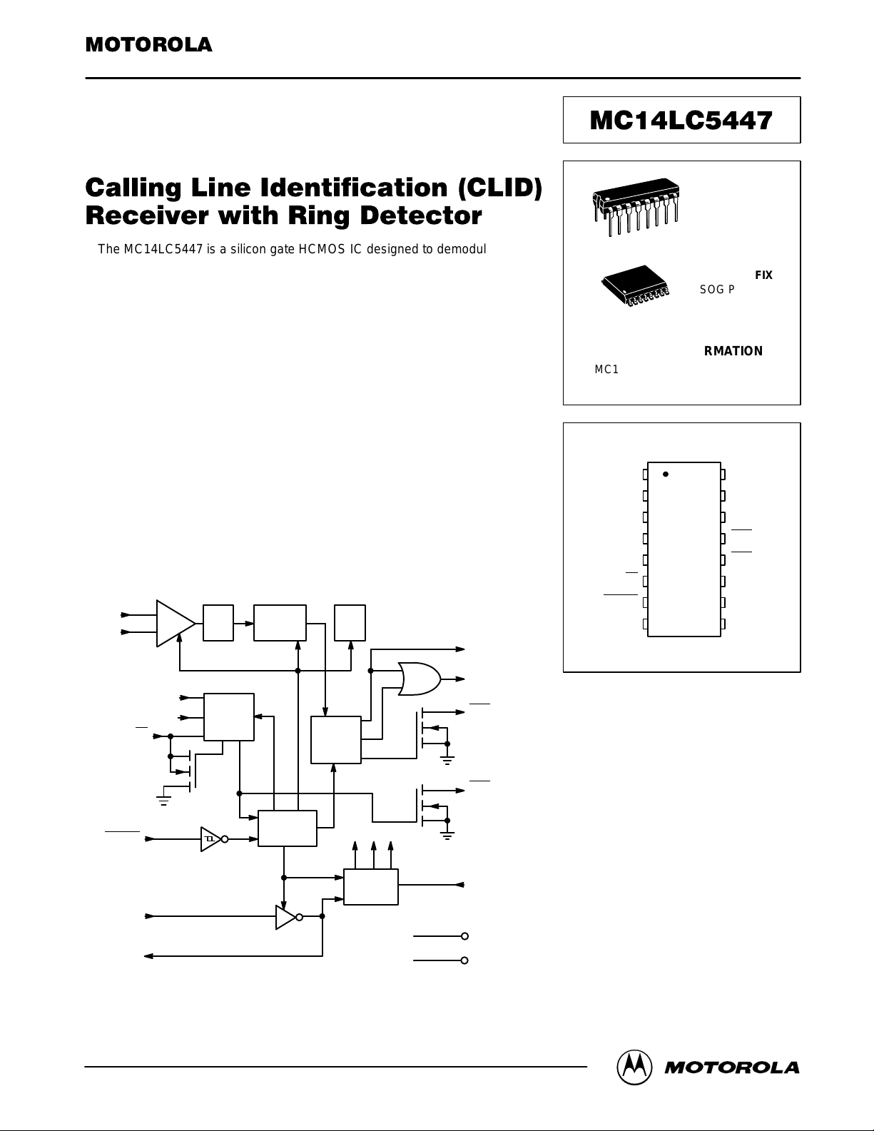
BLOCK DIAGRAM
1
RT
2
–
+
RDI1
RDI2
3
4
6
BPF
RING
DETECT
CIRCUIT
DEMOD
V
AG
VALID
DATA
DETECT
14
15
13
DOR
DOC
CDO
TIP
RING
P SUFFIX
PLASTIC DIP
16
1
16
1
CASE 648
DW SUFFIX
SOG PACKAGE
CASE 751G
ORDERING INFORMATION
MC14LC5447P Plastic DIP
MC14LC5447DW SOG Package
PIN ASSIGNMENT
1
TI
2
RI
3
RDI1
4
RDI2
NC
6
RT
PWRUP
7
8
V
SS
NC = NO CONNECTION
16
15
14
13
125
11
10
9
V
DOC
DOR
CDO
RDO
CLKSIN
OSC
OSC
DD
in
out
12
RDO
INTERNAL
POWER UP
CLOCK
GEN
11
CLKSIN
16
V
DD
8
V
SS
NO CONNECT (5)
MC14LC5447MOTOROLA
in
out
7
10
9
PWRUP
OSC
OSC
This document contains information on a product under development. Motorola reserves the right to change or discontinue this product without notice.
REV 0
7/96
Motorola, Inc. 1996
1
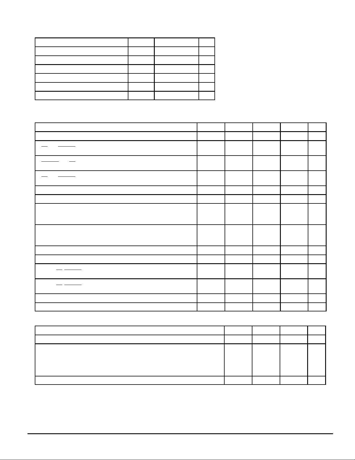
ABSOLUTE MAXIMUM RATINGS
(Voltages referenced to GND, except where noted)
Rating
DC Supply Voltage V
Input Voltage, All Pins V
DC Current Drain Per Pin I ± 10 mA
Power Dissipation P
Operating Temperature Range T
Storage Temperature Range T
Symbol Value Unit
DD
in
D
A
stg
– 0.5 to + 6.0 V
– 0.5 to VDD + 0.5 V
20 mW
0 to + 70 °C
– 40 to + 150 °C
This device contains circuitry to protect the
inputs against damage due to high static voltages or electric fields. However, it is advised that
normal precautions be taken to avoid applications of any voltage higher than maximum rated
voltages to this high impedance circuit. For
proper operation it is recommended that Vin and
V
out
V
out
Reliability of operation is enhanced if unused
inputs are tied to an appropriate logic voltage
level (e.g., either VSS or VDD).
ELECTRICAL CHARACTERISTICS
(All polarities referenced to VSS = 0 V, VDD = + 5 V ± 10%, unless otherwise noted, TA = 0 to + 70°C)
Parameter
DC Supply Voltage V
Supply Current (All Output Pins Unloaded) (See Figure 1)
RT
= 0, PWRUP = 1, XTAL = 3.58 MHz
Supply Current (All Output Pins Unloaded) (See Figure 1)
PWRUP
= 0, RT = Don’t Care, XT AL = 3.58 MHz
Standby Current (All Output Pins Unloaded) (See Figure 1)
RT
= 1, PWRUP = 1
Input Voltage 0 Level (CLKSIN, OSCin) V
Input Voltage 1 Level (CLKSIN, OSCin) V
Output Voltage High: VDD = 5 V (DOR, DOC, OSC
Output Voltage Low: VDD = 5 V (DOR, DOC, OSC
Input Leakage Current (OSCin, CLKSIN, PWRUP, RT, RDI1, and RDI2) I
Output Voltage Low: VDD = 5 V (RDO, RT, CDO) IOL = 2.0 mA V
Input Threshold Voltage Positive Going: VDD = 5 V
(RDI1, RT
Input Threshold Voltage Negative Going: VDD = 5 V
(RDI1, RT
RDI2 Threshold RD2V
TIP/RING Input dc Resistance R
, PWRUP) (See Figure 3)
, PWRUP) (See Figure 3)
out
out
)
IOH = 40 µA
IOH ≤ 1 µA
)
IOL = 1.6 mA
IOL ≤ 1 µA
Symbol Min Typ Max Unit
DD
I
DD
I
DD
I
STBY
IH
V
OH
V
OL
in
OL
V
T+
V
T–
IL
T
in
3.5 5 6 V
— 2.4 3 mA
— 4.0 5.5 mA
— — 1 µA
— — VDD x 0.3 V
VDD x 0.7 — — V
2.4
4.95
— —
— — ±1 µA
— — 0.4 V
2.5 2.75 3.0 V
2.0 2.3 2.6 V
1.0 1.1 1.2 V
— 250 — kΩ
be constrained to the range VSS ≤ (Vin or
) ≤ VDD.
— — V
V
0.4
0.05
ANALOG CHARACTERISTICS (V
Input Sensitivity: TIP and RING (Pins 1 and 2, VDD = + 5 V) – 40 – 45 — dBm
Band–Pass Filter (BPF)
Frequency Response (Relative to 1700 Hz @ 0 dBm) 60 Hz
Carrier Detect Sensitivity — – 48 — dBm
= + 5 V, TA = + 25°C, unless otherwise noted, 0 dBm = 0.7746 Vrms @ 600 Ω)
DD
Characteristic
500 Hz
2700 Hz
≥ 3300 Hz
Min Typ Max Unit
—
—
—
—
– 64
– 4
– 3
– 34
—
dB
—
—
—
MC14LC5447 MOTOROLA
2
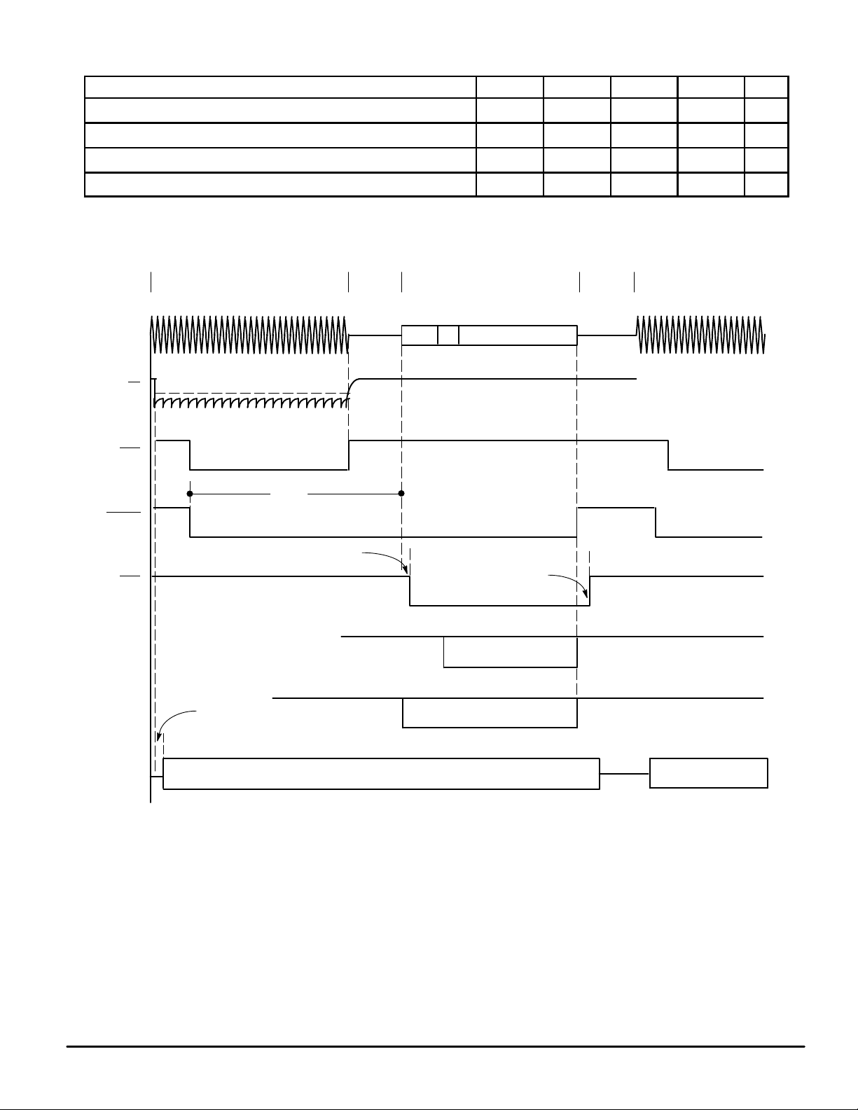
SWITCHING CHARACTERISTICS (V
Description Symbol Min Typ Max Unit
= + 5 V, CL = 50 pF, TA = + 25°C)
DD
OSC Startup (CLKSIN = 1; 3.579 MHz XTAL) t
Power–Up Low to FSK (Setup Time) t
Carrier Detect Acquisition Time t
End of Data to Carrier Detect High t
TIMING DIAGRAM
0.5
SECOND
RI
RT
RDO
2 SECONDS
THRESHOLD TO KEEP PART ON
t
SUPD
DOSC
SUPD
DAQ
DCH
DATA0101 1
— 2 — ms
15 — — ms
— 14 — ms
8 — — ms
0.5
SECOND
PWRUP
CDO
DOC
DOR
OSC
t
DOSC
t
DAQ
COOKED DATA
RAW DATA
CLOCK 3.58 MHz, 3.6864 MHz, OR 455 kHz
t
DCH
MC14LC5447MOTOROLA
3
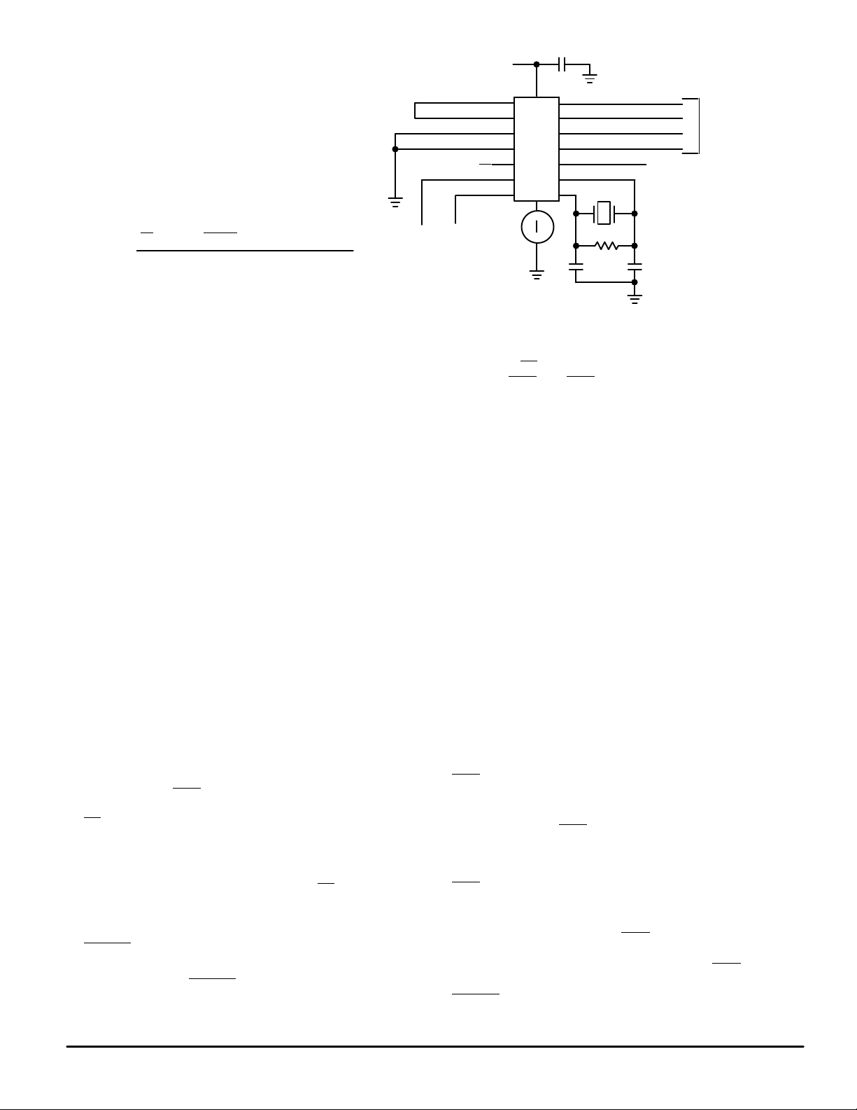
V
TI 1
RI 2
RDI1 3
RDI2 4
NC 5
RT
PWRUP
DD
0.1 µF
15 DOC
16
14 DOR
13 CDO
12 RDO
11 CLKSIN
8
10 OSC
9 OSC
in
out
6
7
V
DD
OPEN
RT
111
0 1 2.4 mA TYP ENABLE
X 0 6.2 mA TYP ENABLE
PWRUP I
µ
A MAX DISABLE
DD
OSC
in
Figure 1. IDD T est Circuit
PIN DESCRIPTIONS
TI
Tip Input (Pin 1)
This input pin is normally connected to the tip side of the
twisted pair. It is internally biased to 1/2 supply voltage when
the device is in the power–up mode. This pin must be dc isolated from the line.
RI
Ring Input (Pin 2)
This input is normally connected to the ring side of the
twisted pair. It is internally biased to 1/2 supply voltage when
the device is in the power–up mode. This pin must be dc isolated from the line.
RDI1
Ring Detect Input 1 (Pin 3)
This input is normally coupled to one of the twisted pair
wires through an attenuating network. It detects energy on
the line and enables the oscillator and precision ring detection circuitry.
RDI2
Ring Detect Input 2 (Pin 4)
This input to the precision ring detection circuit is normally
coupled to one of the twisted pair wires through an attenuating network. A valid ring signal as determined from this
input sends the RDO
RT
Ring Time (Pin 6)
An RC network may be connected to this pin. The RC time
constant is chosen to hold this pin voltage below 2.2 V between the peaks of the ringing signal. RT
power–up control and activates only the circuitry necessary
to determine if the incoming ring is valid.
PWRUP
Power Up (Pin 7)
A logic 0 on the PWRUP
the active mode ready to demodulate incoming data. A
(Pin 12) to a logic 0.
is an internal
input causes the device to be in
3.579 MHz
Ω
10 M
30
pF
30
pF
logic 1 on this pin causes the device to be in the standby
mode, if the RT
trolled by RDO
input pin is at a logic 1. This pin may be con and CDO for auto power–up operation. For
other applications, this pin may be controlled externally .
V
SS
Ground (Pin 8)
Ground return pin is typically connected to the system
ground.
OSC
out
Oscillator Output (Pin 9)
This pin will have either a crystal or a ceramic resonator
tied to it with the other end connected to OSCin.
OSC
in
Oscillator Input (Pin 10)
This pin will have either a crystal or a ceramic resonator
tied to it with the other end connected to OSC
. OSCin may
out
also be driven directly from an appropriate external source.
CLKSIN
Clock Select Input (Pin 11)
A logic 1 on this input configures the device to accept either a 3.579 MHz or 3.6864 MHz crystal. A logic 0 on this pin
configures the part to operate with a 455 kHz resonator.
For crystal and resonator specifications see Table 1.
RDO
Ring Detect Out (Pin 12)
This open–drain output goes low when a valid ringing
signal is detected. RDO
remains low as long as the ringing
signal remains valid. This signal can be used for auto power–
up, when connected to Pin 7.
CDO
Carrier Detect Output (Pin 13)
When low, this open drain output indicates that a valid
carrier is present on the line. CDO
remains low as long as
the carrier remains valid. An 8 ms hysteresis is built in to
allow for a momentary drop out of the carrier. CDO
may be
used in the auto power–up configuration when connected to
PWRUP
.
MC14LC5447 MOTOROLA
4
 Loading...