

Order this document by MC14C89B/D
The MC14C89B and MC14C89AB are low monolithic quad line receivers
using bipolar technology, which conform to the EIA–232–E, EIA–562 and
CCITT V.28 Recommendations. The outputs feature LSTTL and CMOS
compatibility for easy interface to +5.0 V digital systems. Internal
time–domain filtering eliminates the need for external filter capacitors in most
cases.
The MC14C89B has an input hysteresis of 0.35 V , while the MC14C89AB
hysteresis is 0.95 V. The response control pins allow adjustment of the
threshold level if desired. Additionally, an external capacitor may be added
for additional noise filtering.
The MC14C89B and MC14C89AB are available in both a 14 pin
dual–in–line plastic DIP and SOIC package.
Features:
• Low Power Consumption
• Meets EIA–232–E, EIA–562, and CCITT V.28 Recommendations
• TTL/CMOS Compatible Outputs
• Standard Power Supply: + 5.0 V ±10%
• Pin Equivalent to MC1489, MC1489A, TI’s SN75C189/A, SN75189/A
and National Semiconductor’s DS14C89/A
• External Filtering Not Required in Most Cases
• Threshold Level Externally Adjustable
• Hysteresis: 0.35 V for MC14C89B, 0.95 V for MC14C89AB
• Available in Plastic DIP, and Surface Mount Packaging
• Operating Ambient Temperature: –40° to +85°C
QUAD LOW POWER
LINE RECEIVERS
SEMICONDUCTOR
TECHNICAL DATA
P SUFFIX
PLASTIC PACKAGE
CASE 646
D SUFFIX
PLASTIC PACKAGE
CASE 751A
(SO–14)
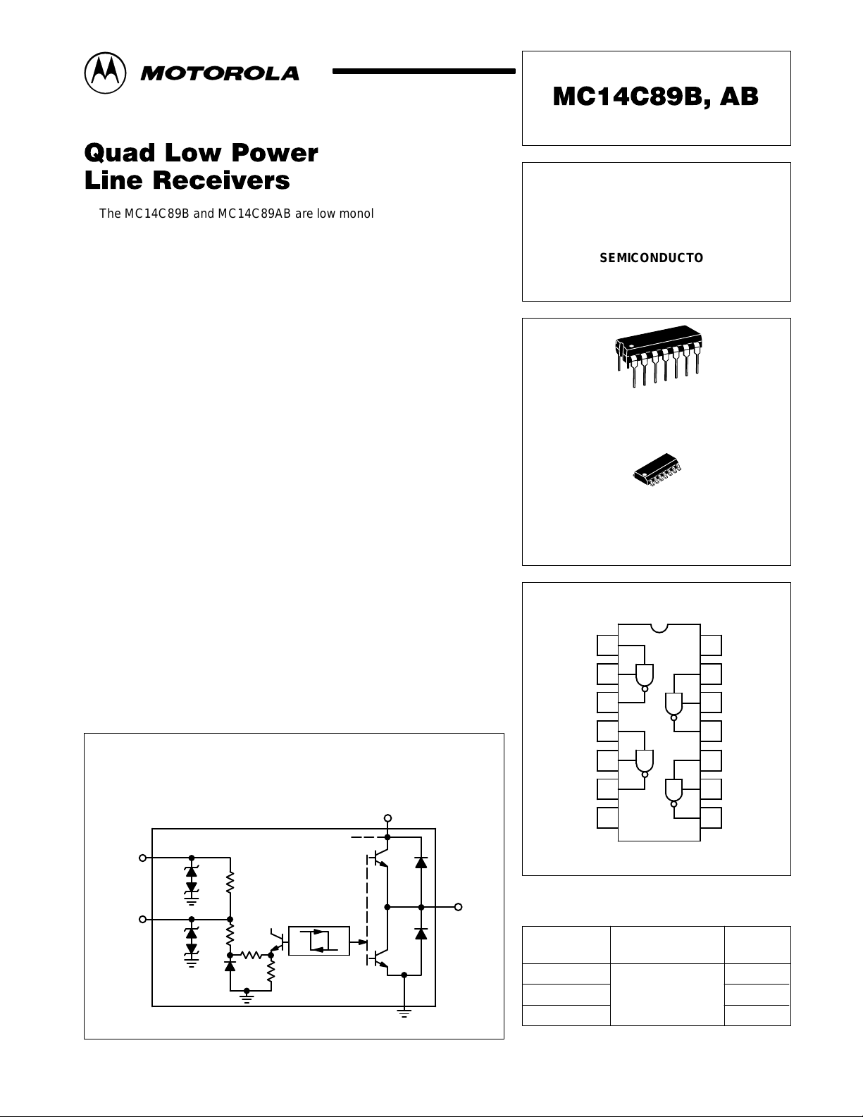
PIN CONNECTIONS
Representative Block Diagram
(Each Receiver)
Input
Response
Control
MOTOROLA ANALOG IC DEVICE DATA
1
Input A
Response
Control A
Output A
Response
Control B
Output B
V
CC
Output
Ground
Device
MC14C89BP
MC14C89ABP Plastic DIP
MC14C89ABD SO–14
Motorola, Inc. 1996 Rev 0
2
3
4
Input B
5
6
7
(Top View)
ORDERING INFORMATION
Operating
Temperature Range
TA = – 40° to +85°C
14
13
12
11
10
9
8
V
CC
Input D
Response
Control D
Output D
Input C
Response
Control C
Output C
Package
Plastic DIP
1
MC14C89B, AB
MAXIMUM RATINGS
Rating Symbol Value Unit
Power Supply Voltage
V
CC(max)
V
CC(min)
Input Voltage V
Output Load Current I
Junction Temperature T
Devices should not be operated at these limits. The “Recommended Operating Conditions” table provides
for actual device operation.
V
CC
in
O
J
+ 7.0
– 0.5
± 30 Vdc
Self–Limiting –
–65, +150 °C
RECOMMENDED OPERATING CONDITIONS
Characteristic Symbol Min Typ Max Unit
Power Supply Voltage V
Input Voltage V
Output Current Capability I
Operating Ambient Temperature T
All limits are not necessarily functional concurrently.
CC
in
O
A
Vdc
4.5 5.0 5.5 Vdc
–25 – 25 Vdc
–7.5 – 6.0 mA
–40 – 85 °C
ELECTRICAL CHARACTERISTICS (–40°C
Characteristic
Supply Current (I
ICC @ +4.5 V VCC +5.5 V
Output Voltage – High, Vin 0.4 V (See Figures 2 and 3)
I
= –20 µAVCC = 4.5 V
out
I
= –3.2 mA VCC = 4.5 V
out
Output Voltage – Low, Vin 2.4 V
I
= 3.2 mA VCC = 4.5 V
out
Output Short Circuit Current** (VCC = 5.5 V, see Figure 4)
Normally High Output shorted to ground
Normally Low Output shorted to V
Input Threshold Voltage (VCC = 5.0 V)
(MC14C89AB, see Figure 5) Low Level
(MC14C89B, see Figure 6)
Input Impedance (+4.5 V VCC +5.5 V –25 V Vin +25 V) 3.0 5.5 7.0 kΩ
* * Typicals reflect performance @ TA = 25°C
**Only one output shorted at a time, for not more than 1.0 seconds.
TIMING CHARACTERISTICS (T
Output Transition Time (10% to 90%)
4.5 V VCC 5.5 V
Propagation Delay Time
4.5 V VCC 5.5 V
Input Noise Rejection (see Figure 9) 1.0 1.5 – µs
Output Low–to–High
Output High–to–Low
out = 0
)
VCC = 5.5 V
VCC = 5.5 V
VCC = 5.5 V
High Level
Low Level
High Level
A
Characteristic
CC
= +25°C, unless otherwise noted.)
TA +85°C, unless otherwise noted.)*
Symbol Min Typ Max Unit
I
CC
V
OH
V
OL
I
OS
V
IL
V
IH
V
IL
V
IH
Symbol Min Typ Max Unit
t
T
t
PLH
t
PHL
– 330 700
3.5
3.5
2.5
2.5
–
–
–35
–
0.75
1.6
0.75
1.0
– 0.08 0.30 µs
–
–
3.8
4.8
3.7
4.7
0.1
0.1
–13.9
+10.3
0.95
1.90
0.95
1.3
3.35
2.55
–
–
–
–
0.4
0.4
–
35
1.25
2.25
1.25
1.5
6.0
6.0
µA
Vdc
mA
Vdc
µs
2
MOTOROLA ANALOG IC DEVICE DATA

S.G.
MC14C89B, AB
Figure 1. Timing Diagram
3.0 V
1.5 V
V
CC
S.G.
NOTES: S.G. set to: f = 20 kHz;
50 pF
RC
(Open)
Duty Cycle = 50%;
tr, tf p 5.0 ns
V
out
0 V
V
out
t
PHL
t
PLH
90%
50%
10%
t
T
50%
t
T
STANDARDS COMPLIANCE
The MC14C89B and MC14C89AB are designed to comply
with EIA–232–E (formerly RS–232), the newer EIA–562
(which is a higher speed version of the EIA–232), and CCITT
V.28 Recommendations. EIA–562 was written around
modern integrated circuit technology, whereas EIA–232
electro–mechanical circuitry in use at the time of its creation.
Yet the user will find enough similarities to allow a certain
amount of compatibility among equipment built to the two
standards. Following is a summary of the key specifications
relating to the systems and the receivers.
retains many of the specifications written around the
Parameter EIA–232–E EIA–562
Max Data Rate 20 kBaud 38.4 kBaud Asynchronous
Max Cable Length 50 feet Based on cable capacitance/data rate
Transition Region –3.0 V to +3.0 V –3.0 V to +3.0 V
MARK (one, off) More negative than –3.0 V More negative than –3.3 V
SPACE (zero, on) More positive than +3.0 V More positive than +3.3 V
Fail Safe Output = Binary 1 Output = Binary 1
Open Circuit Input Voltage
Slew Rate (at the driver)
Loaded Output Voltage (at the driver) 5.0 V p VOp 15 V for loads between
t
2.0V Not Specified
p
30 V/µs anywhere on the waveform
3.0 kΩ and 7.0 kΩ
64 kBaud Synchronous
p
30 V/µs anywhere on the waveform,
q
4.0 V/µs between +3.0 V and –3.0 V
VO q 3.7 V for a load of 3.0 kΩ
V
V
OH
OL
Figure 2. T ypical Output versus Supply Voltage Figure 3. T ypical Output Voltage versus Temperature
, OUTPUT VOL TAGE (V)
O
V
5.0
4.0
3.0
2.0
1.0
0
4.5
VOH(I
= –20 µA)
out
VOH(I
= –3.2 mA)
out
VOL(I
= 3.2 mA)
out
VCC, SUPPLY VOLTAGE (V)
MC14C89AB
MC14C89B
°
C
TA = 25
5.55.35.14.94.7
, OUTPUT VOL TAGE (V)
O
V
5.0
4.0
3.0
2.0
1.0
0
–40
VOH(I
= –20 µA)
out
VOH(I
= –3.2 mA)
out
VOL(I
= 3.2 mA)
out
25
TA, AMBIENT TEMPERATURE (
MC14C89AB
MC14C89B
VCC = 5 V
57.5–7.5 85
°
C)
MOTOROLA ANALOG IC DEVICE DATA
3

MC14C89B, AB
15
10
5.0
–5.0
SHORT CIRCUIT CURRENT (mA)
–10
–15
2.0
1.8
1.6
1.4
1.2
Figure 4. Typical Short Circuit Current
versus T emperature
2.0
Normally Low Output Shorted to V
0
Normally High Output Shorted to Ground
TA, AMBIENT TEMPERATURE (
CC
MC14C89AB
MC14C89B
VCC = 5.5 V
°
C)
8557.525–7.5–40
1.8
1.6
1.4
1.2
1.0
INPUT THRESHOLD VOLTAGE (Vdc)
0.8
Figure 6. T ypical Threshold Voltage
versus T emperature
MC14C89B
t
VCC t 5.5 V
4.5 V
V
IH
5.0
4.0
3.0
2.0
Figure 5. T ypical Threshold Voltage
versus T emperature
V
IH
MC14C89AB
t
VCC t 5.5 V
4.5 V
V
IL
–7.5–40
TA, AMBIENT TEMPERATURE (
25
°
C)
Figure 7. T ypical Effect of Response
Control Pin Bias
VIL @ V
bat
VIL @ V
= –10 V
= –3.0 V
bat
8557.5
RC
R
RC
+
V
bat
–
1.0
INPUT THRESHOLD VOLTAGE (Vdc)
0.8
V
IL
TA, AMBIENT TEMPERATURE (
5.0
4.5
4.0
3.5
3.0
, PULSE AMPLITUDE (V)E
in
2.5
2.0
1.0
INPUT THRESHOLD VOLTAGE (Vdc)
8557.525–7.5–40
°
C)
0
Nominal V
0
10 k
Figure 8. T ypical Noise Pulse Rejection
MC14C89AB
MC14C89B
Pulse Rate = 300 kHz
RC Pin Open
Noise Pulse Rejection
1.61.4
1.8
PW, INPUT PULSE WIDTH (
µ
s)
IL
Ω
Ω
20 k
BIAS RESISTANCE (RRC)
2.82.62.42.22.0
4.5 V t VCC t 5.5 V
30 k
Ω
40 k
Ω
50 k
Ω
4
MOTOROLA ANALOG IC DEVICE DATA

MC14C89B, AB
APPLICATIONS INFORMATION
Description
The MC14C89AB and MC14C89B are designed to be
direct replacements for the MC1489A and MC1489. Both
devices meet all EIA–232 specifications and also the faster
EIA–562 and CCITT V.28 specifications. Noise pulse
rejection circuitry eliminates the need for most response
control filter capacitors but does not exclude the possibility as
filtering is still possible at the Response Control (RC) pins.
Also, the Response Control pins allow for a user defined
selection of the threshold voltages. The MC14C89AB and
MC14C89B are manufactured with a bipolar technology
using low power techniques and consume at most 700 mA,
plus load currents with a +5.0 V supply .
Outputs
The output low or high voltage depends on the state of the
inputs, the load current, the bias of the Response Control
pins, and the supply voltage. T able 1 applies to each receiver ,
regardless of how many other receivers within the package
are supplying load current.
T able 1. Function Table
Receivers
Input* Output*
H
L
*The asterisk denotes A, B, C, or D.
Receiver Inputs and Response Control
The receiver inputs determine the state of the outputs in
accordance with Table 1. The nominal VIL and V
thresholds are 0.95 V and 1.90 V respectively for the
MC14C89AB. For the MC14C89B, the nominal VIL and V
thresholds are 0.95 and 1.30, respectively. The inputs are
able to withstand ± 30 V referenced to ground. Should the
input voltage exceed ground by more than ±30 V , excessive
currents will flow at the input pin. Open input pins will
generate a logic high output, but good design practices
dictate that inputs should never be left open.
The Response Control (RC) pins are coupled to the inputs
through a resistor string. The RC pins provide for adjustment
of the threshold voltages of the IC while preserving the
amount of hysteresis. Figure 10 shows a typical application
to adjust the threshold voltages. The RC pins also provide
access to an internal resistor string which permits low pass
filtering of the input signal within the IC. Like the input pins,
the RC pins should not be taken above or below ground by
more than ±30 V or excessive currents will flow at these pins.
The dependence of the low level threshold voltage (VIL) upon
RRC and V
VIL]
ȡ
ȧ
ȧ
can be described by the following equation:
bat
V
*
V
NJ
0.09
5.32 kW)
505
ƪ
bat
RRC(1.6))2.02 k
6.67 106W
R
RC
W
Ȣ
VIH can be found by calculating for VIL using equation (1)
then adding the hysteresis for each device (0.35 for the
L
H
IH
IH
505
W
2
ȣ
ȧ
ȧ
(1)
ƫ
Nj
W
Ȥ
MC14C89B or 0.95 V for the MC14C89AB). Figure 7 plots
equation (1) for two values of V
If an RC pin is to be used for low pass filtering, the
capacitor chosen can be calculated by the equation,
CRC]
where f
of the low pass filter.
Another feature of the MC14C89AB and MC14C89B is
input noise rejection. The inputs have the ability to ignore
pulses which exceed the VIH and VIL thresholds but are less
than 1.0 ms in duration. As the duration of the pulse exceeds
1.0 ms, the noise pulse may still be ignored depending on its
amplitude. Figure 8 is a graph showing typical input noise
rejection as a function of pulse amplitude and pulse duration.
Figure 8 reflects data taken for an input with an unconnected
RC pin and applied to the MC14C89AB and MC14C89B.
Operating Temperature Range
The ambient operating temperature range is listed as
–40°C to +85°C, and the devices are designed to meet the
EIA–232–E, EIA–562 and CCITT V.28 specifications over
this temperature range. The timing characteristics are
guaranteed to meet the specifications at +25°C. The
maximum ambient operating temperature is listed as +85°C.
However, a lower ambient may be required depending on
system use (i.e., specifically how many receivers within a
package are used), and at what current levels they are
operating. The maximum power which may be dissipated
within the package is determined by:
where: R
where: VCC =
VOH, VOL =
As indicated, the first term (in brackets) must be calculated
and summed for each of the four receivers, while the last
term is common to the entire package.
represents the desired –3 dB role–off frequency
–3dB
Figure 9. Application to Adjust Thresholds
θJA
T
J(max)
TA =
PD =
ICC =
2.02 kW2pf
Input Pin
P
D
thermal resistance (typ., 100°C/W for the
=
DIP and 125°C/W for the SOIC packages);
maximum operating junction temperature
=
(150°C); and
ambient temperature.
{[(VCC – VOH)IOH] or
[(VOL)IOL]}
positive supply voltage;
measured or estimated from Figure 2
and 3;
measured quiescent supply current.
(max)
+
and a range of RRC.
bat
1
*
3dB
Response Control Pin
R
RC
+
V
bat
–
T
J(max)–TA
R
q
JA
each receiver +
(VCC
(2)
ICC)
MOTOROLA ANALOG IC DEVICE DATA
5

–T–
SEATING
PLANE
MC14C89B, AB
OUTLINE DIMENSIONS
P SUFFIX
PLASTIC PACKAGE
CASE 646–06
ISSUE L
14 8
B
17
A
F
N
SEATING
HG D
PLANE
–A–
14 8
–B–
P 7 PL
71
G
C
D 14 PL
0.25 (0.010) A
K
M
S
B
T
C
K
L
J
M
D SUFFIX
PLASTIC PACKAGE
CASE 751A–03
(SO–14)
ISSUE F
R X 45
M
_
0.25 (0.010) B
M
S
NOTES:
1. LEADS WITHIN 0.13 (0.005) RADIUS OF TRUE
POSITION AT SEATING PLANE AT MAXIMUM
MATERIAL CONDITION.
2. DIMENSION L TO CENTER OF LEADS WHEN
FORMED PARALLEL.
3. DIMENSION B DOES NOT INCLUDE MOLD
FLASH.
4. ROUNDED CORNERS OPTIONAL.
DIM MIN MAX MIN MAX
A 0.715 0.770 18.16 19.56
B 0.240 0.260 6.10 6.60
C 0.145 0.185 3.69 4.69
D 0.015 0.021 0.38 0.53
F 0.040 0.070 1.02 1.78
G 0.100 BSC 2.54 BSC
H 0.052 0.095 1.32 2.41
J 0.008 0.015 0.20 0.38
K 0.115 0.135 2.92 3.43
L 0.300 BSC 7.62 BSC
M 0 10 0 10
____
N 0.015 0.039 0.39 1.01
NOTES:
1. DIMENSIONING AND TOLERANCING PER ANSI
Y14.5M, 1982.
2. CONTROLLING DIMENSION: MILLIMETER.
3. DIMENSIONS A AND B DO NOT INCLUDE
MOLD PROTRUSION.
4. MAXIMUM MOLD PROTRUSION 0.15 (0.006)
PER SIDE.
5. DIMENSION D DOES NOT INCLUDE DAMBAR
M
F
J
PROTRUSION. ALLOWABLE DAMBAR
PROTRUSION SHALL BE 0.127 (0.005) TOTAL
IN EXCESS OF THE D DIMENSION AT
MAXIMUM MATERIAL CONDITION.
DIM MIN MAX MIN MAX
A 8.55 8.75 0.337 0.344
B 3.80 4.00 0.150 0.157
C 1.35 1.75 0.054 0.068
D 0.35 0.49 0.014 0.019
F 0.40 1.25 0.016 0.049
G 1.27 BSC 0.050 BSC
J 0.19 0.25 0.008 0.009
K 0.10 0.25 0.004 0.009
M 0 7 0 7
____
P 5.80 6.20 0.228 0.244
R 0.25 0.50 0.010 0.019
MILLIMETERSINCHES
INCHESMILLIMETERS
Motorola reserves the right to make changes without further notice to any products herein. Motorola makes no warranty , representation or guarantee regarding
the suitability of its products for any particular purpose, nor does Motorola assume any liability arising out of the application or use of any product or circuit, and
specifically disclaims any and all liability, including without limitation consequential or incidental damages. “T ypical” parameters which may be provided in Motorola
data sheets and/or specifications can and do vary in different applications and actual performance may vary over time. All operating parameters, including “Typicals”
must be validated for each customer application by customer’s technical experts. Motorola does not convey any license under its patent rights nor the rights of
others. Motorola products are not designed, intended, or authorized for use as components in systems intended for surgical implant into the body, or other
applications intended to support or sustain life, or for any other application in which the failure of the Motorola product could create a situation where personal injury
or death may occur. Should Buyer purchase or use Motorola products for any such unintended or unauthorized application, Buyer shall indemnify and hold Motorola
and its officers, employees, subsidiaries, affiliates, and distributors harmless against all claims, costs, damages, and expenses, and reasonable attorney fees
arising out of, directly or indirectly, any claim of personal injury or death associated with such unintended or unauthorized use, even if such claim alleges that
Motorola was negligent regarding the design or manufacture of the part. Motorola and are registered trademarks of Motorola, Inc. Motorola, Inc. is an Equal
Opportunity/Affirmative Action Employer.
How to reach us:
USA/EUROPE/ Locations Not Listed: Motorola Literature Distribution; JAPAN: Nippon Motorola Ltd.; Tatsumi–SPD–JLDC, 6F Seibu–Butsuryu–Center,
P.O. Box 20912; Phoenix, Arizona 85036. 1–800–441–2447 or 602–303–5454 3–14–2 Tatsumi Koto–Ku, Tokyo 135, Japan. 03–81–3521–8315
MFAX: RMF AX0@email.sps.mot.com – TOUCHT ONE 602–244–6609 ASIA / PACIFIC: Motorola Semiconductors H.K. Ltd.; 8B Tai Ping Industrial Park,
INTERNET: http://Design–NET.com 51 Ting Kok Road, Tai Po, N.T., Hong Kong. 852–26629298
6
◊
MOTOROLA ANALOG IC DEVICE DATA
MC14C89B/D
*MC14C89B/D*
 Loading...