

MOTOROLA MC14C89ABDR2 Datasheet
Device
Operating
Temperature Range
Package
SEMICONDUCTOR
TECHNICAL DATA
QUAD LOW POWER
LINE RECEIVERS
ORDERING INFORMATION
MC14C89BP
TA = – 40° to +85°C
Plastic DIP
Order this document by MC14C89B/D
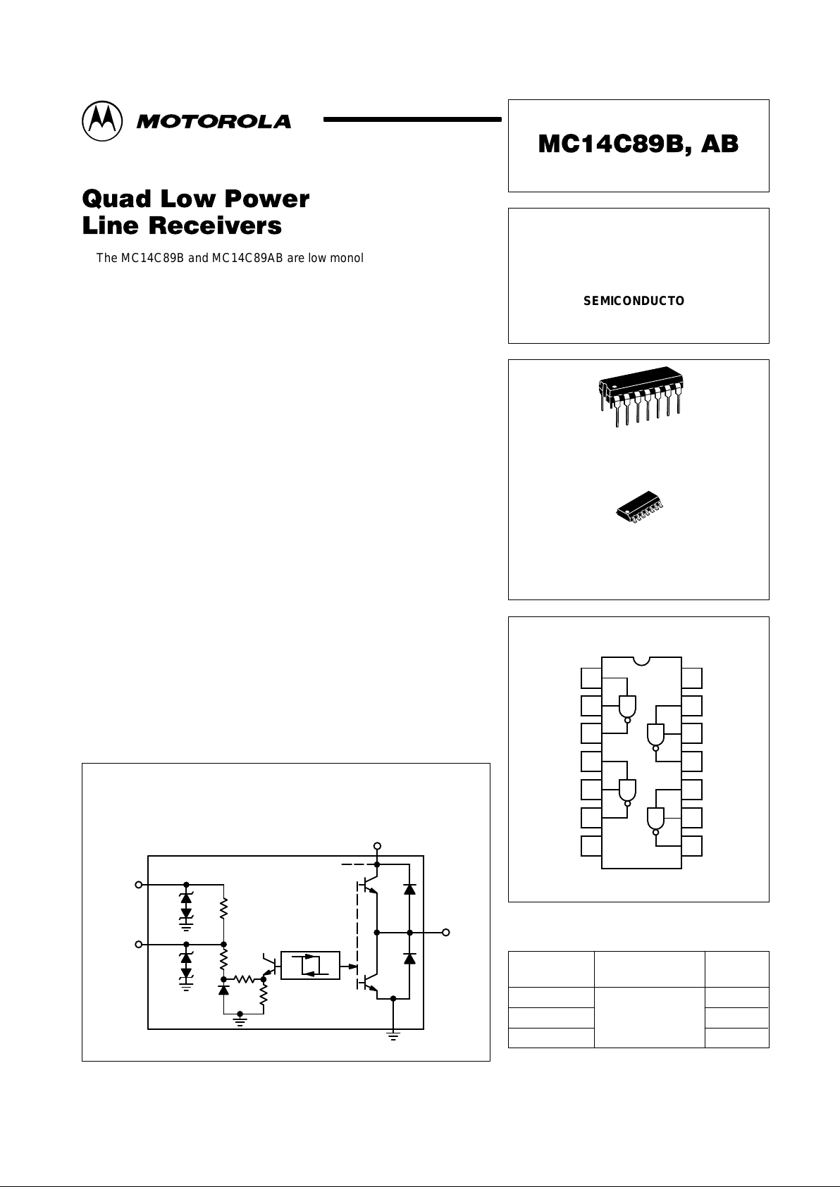
PIN CONNECTIONS
P SUFFIX
PLASTIC PACKAGE
CASE 646
D SUFFIX
PLASTIC PACKAGE
CASE 751A
(SO–14)
(Top View)
Ground
9
10
11
12
14
13
7
6
5
4
3
1
2
8
Output A
Input A
Input B
Output B
Input D
V
CC
Output D
Output C
Response
Control D
Input C
Response
Control C
Response
Control B
Response
Control A
MC14C89ABP Plastic DIP
MC14C89ABD SO–14
1
MOTOROLA ANALOG IC DEVICE DATA
The MC14C89B and MC14C89AB are low monolithic quad line receivers
using bipolar technology, which conform to the EIA–232–E, EIA–562 and
CCITT V.28 Recommendations. The outputs feature LSTTL and CMOS
compatibility for easy interface to +5.0 V digital systems. Internal
time–domain filtering eliminates the need for external filter capacitors in most
cases.
The MC14C89B has an input hysteresis of 0.35 V , while the MC14C89AB
hysteresis is 0.95 V. The response control pins allow adjustment of the
threshold level if desired. Additionally, an external capacitor may be added
for additional noise filtering.
The MC14C89B and MC14C89AB are available in both a 14 pin
dual–in–line plastic DIP and SOIC package.
Features:
• Low Power Consumption
• Meets EIA–232–E, EIA–562, and CCITT V.28 Recommendations
• TTL/CMOS Compatible Outputs
• Standard Power Supply: + 5.0 V ±10%
• Pin Equivalent to MC1489, MC1489A, TI’s SN75C189/A, SN75189/A
and National Semiconductor’s DS14C89/A
• External Filtering Not Required in Most Cases
• Threshold Level Externally Adjustable
• Hysteresis: 0.35 V for MC14C89B, 0.95 V for MC14C89AB
• Available in Plastic DIP, and Surface Mount Packaging
• Operating Ambient Temperature: –40° to +85°C
Representative Block Diagram
(Each Receiver)
Input
V
CC
Output
Response
Control
Motorola, Inc. 1996 Rev 0
MC14C89B, AB
2
MOTOROLA ANALOG IC DEVICE DATA
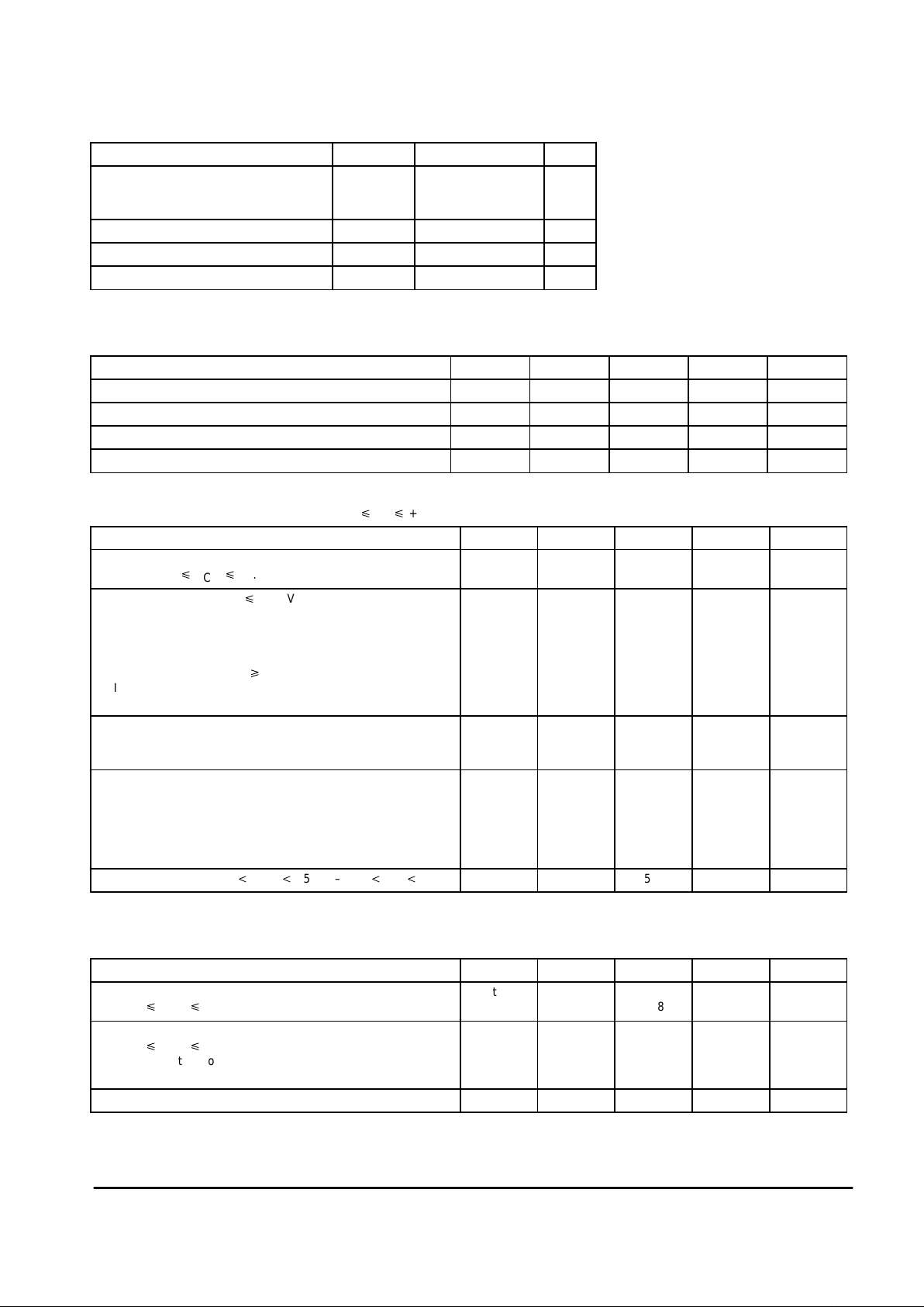
MAXIMUM RATINGS
Rating Symbol Value Unit
Power Supply Voltage
V
CC(max)
V
CC(min)
V
CC
+ 7.0
– 0.5
Vdc
Input Voltage V
in
± 30 Vdc
Output Load Current I
O
Self–Limiting –
Junction Temperature T
J
–65, +150 °C
Devices should not be operated at these limits. The “Recommended Operating Conditions” table provides
for actual device operation.
RECOMMENDED OPERATING CONDITIONS
Characteristic Symbol Min Typ Max Unit
Power Supply Voltage V
CC
4.5 5.0 5.5 Vdc
Input Voltage V
in
–25 – 25 Vdc
Output Current Capability I
O
–7.5 – 6.0 mA
Operating Ambient Temperature T
A
–40 – 85 °C
All limits are not necessarily functional concurrently.
ELECTRICAL CHARACTERISTICS (–40°C
TA +85°C, unless otherwise noted.)*
Characteristic
Symbol Min Typ Max Unit
Supply Current (I
out = 0
)
ICC @ +4.5 V VCC +5.5 V
I
CC
– 330 700
µA
Output Voltage – High, Vin 0.4 V (See Figures 2 and 3)
I
out
= –20 µAVCC = 4.5 V
VCC = 5.5 V
I
out
= –3.2 mA VCC = 4.5 V
VCC = 5.5 V
Output Voltage – Low, Vin 2.4 V
I
out
= 3.2 mA VCC = 4.5 V
VCC = 5.5 V
V
OH
V
OL
3.5
3.5
2.5
2.5
–
–
3.8
4.8
3.7
4.7
0.1
0.1
–
–
–
–
0.4
0.4
Vdc
Output Short Circuit Current** (VCC = 5.5 V , see Figure 4)
Normally High Output shorted to ground
Normally Low Output shorted to V
CC
I
OS
–35
–
–13.9
+10.3
–
35
mA
Input Threshold Voltage (VCC = 5.0 V)
(MC14C89AB, see Figure 5) Low Level
High Level
(MC14C89B, see Figure 6)
Low Level
High Level
V
IL
V
IH
V
IL
V
IH
0.75
1.6
0.75
1.0
0.95
1.90
0.95
1.3
1.25
2.25
1.25
1.5
Vdc
Input Impedance (+4.5 V VCC +5.5 V –25 V Vin +25 V) 3.0 5.5 7.0 kΩ
* * Typicals reflect performance @ TA = 25°C
**Only one output shorted at a time, for not more than 1.0 seconds.
TIMING CHARACTERISTICS (T
A
= +25°C, unless otherwise noted.)
Characteristic
Symbol Min Typ Max Unit
Output Transition Time (10% to 90%)
4.5 V VCC 5.5 V
t
T
– 0.08 0.30 µs
Propagation Delay Time
4.5 V VCC 5.5 V
Output Low–to–High
Output High–to–Low
t
PLH
t
PHL
–
–
3.35
2.55
6.0
6.0
µs
Input Noise Rejection (see Figure 9) 1.0 1.5 – µs
 Loading...