

Device
Operating
Temperature Range
Package
SEMICONDUCTOR
TECHNICAL DATA
QUAD LOW POWER
LINE DRIVER
ORDERING INFORMATION
MC14C88BP
MC14C88BD
TA = – 40° to +85°C
Plastic DIP
SO–14
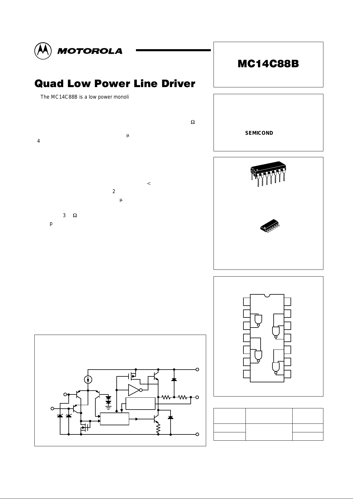
PIN CONNECTIONS
Order this document by MC14C88B/D
P SUFFIX
PLASTIC PACKAGE
CASE 646
D SUFFIX
PLASTIC PACKAGE
CASE 751A
(SO–14)
(Top View)
Output A
Input A
1
V
EE
2
3
Input B1
Input B2
Output B
Gnd
4
5
6
7
14
Input D1
Input D2
12
13
V
CC
Input C1
Output D
Input C2
Output C
8
9
11
10
1
MOTOROLA ANALOG IC DEVICE DATA
The MC14C88B is a low power monolithic quad line driver, using BiMOS
technology, which conforms to EIA–232–D, EIA–562, and CCITT V.28. The
inputs feature TTL and CMOS compatibility with minimal loading. The
outputs feature internally controlled slew rate limiting, eliminating the need
for external capacitors. Power off output impedance exceeds 300 W, and
current limiting protects the outputs in the event of short circuits.
Power supply current is less than 160 mA over the supply voltage range of
±4.5 to ±15 V. EIA–232–D performance is guaranteed with a minimum
supply voltage of ±6.5 V.
The MC14C88B is pin compatible with the MC1488, SN75188,
SN75C188, DS1488, and DS14C88. This device is available in 14 pin plastic
DIP, and surface mount packaging.
Features:
• BiMOS Technology for Low Power Operation (
t
5.0 mW)
• Meets Requirements of EIA–232–D, EIA–562, and CCITT V.28
• Quiescent Current Less Than 160
m
A
• TTL/CMOS Compatible Inputs
• Minimum 300
W
Output Impedance when Powered Off
• Supply Voltage Range: ±4.5 to ±15 V
• Pin Equivalent to MC1488
• Current Limited Output: 10 mA Minimum
• Operating Ambient Temperature: –40° to 85°C
Representative Block Diagram
(Each Driver)
V
EE
39 39
Switching
Control
Output250
V
CC
Slew Rate
Control
45
Input 2
Input 1
Motorola, Inc. 1996 Rev 0
MC14C88B
2
MOTOROLA ANALOG IC DEVICE DATA
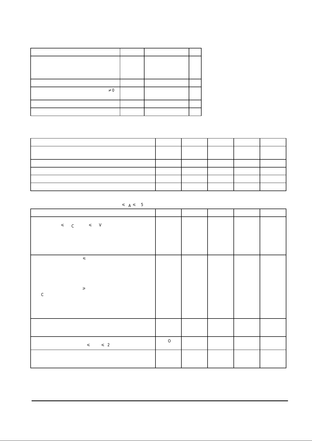
MAXIMUM RATINGS (T
A
= +25°C, unless otherwise noted.)
Rating Symbol Value Unit
Power Supply Voltage
V
CC(max)
V
EE(min)
(VCC – VEE)
max
V
CC
V
EE
VCC – V
EE
+17
–17
34
Vdc
Input Voltage (All Inputs) V
in
VEE–0.3, VEE+39 Vdc
Applied Output Voltage, when VCC=VEE0
0 V
Applied Output Voltage, when VCC=VEE=0 V
V
X
VEE–6.0 V , VCC+6.0 V
±15
Vdc
Output Current I
O
Self Limiting mA
Operating Junction Temperature T
J
– 65, + 150 °C
Devices should not be operated at these limits. The “Recommended Operating Conditions” table provides
for actual device operation.
RECOMMENDED OPERATING CONDITIONS
Characteristic Symbol Min Typ Max Unit
Power Supply Voltage V
CC
V
EE
+4.5
–15
–
–
+15
–4.5
Vdc
Input Voltage (All Inputs) V
in
0 – V
CC
Vdc
Applied Output Voltage (VCC=VEE=0 V) V
O
–2.0 0 +2.0 Vdc
Output DC Load R
L
3.0 – 7.0 kΩ
Operating Ambient Temperature Range T
A
–40 – +85 °C
All limits are not necessarily functional concurrently.
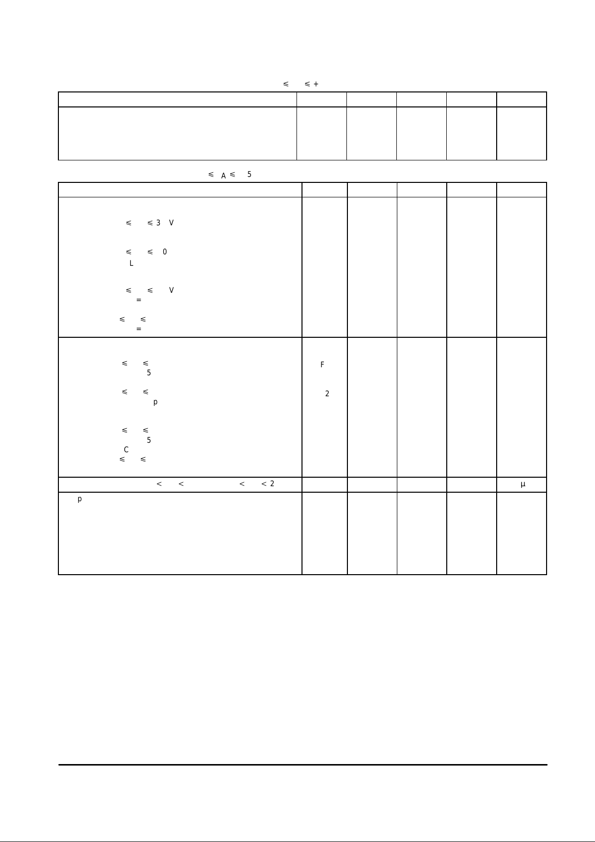
ELECTRICAL CHARACTERISTICS (–40°C
p
TA p+85°C, unless otherwise noted.)*
Characteristic Symbol Min Typ Max Unit
Supply Current (I
out
= 0, see Figure 2)
ICC @ 4.75 V p VCC, –VEE p 15 V
Outputs High
Outputs Low
I
EE
Outputs High
Outputs Low
ICC
(OH)
ICC
(OL)
IEE
(OH)
IEE
(OL)
–
–
–160
–160
–
–
–
–
160
160
–
–
µA
Output Voltage – High, Vin p0.8 V (RL = 3.0 kΩ , see Fi gure 3)
VCC = +4.75 V , VEE = –4.75 V
VCC = +5.0 V , VEE = –5.0 V
VCC = +6.5 V , VEE = –6.5 V
VCC = +12 V , VEE = –12 V
VCC = +13.2 V , VEE = –13.2 V (RL = ∞)
Output Voltage – Low, Vin q2.0 V
VCC = +4.75 V , VEE = –4.75 V
VCC = +5.0 V , VEE = –5.0 V
VCC = +6.5 V , VEE = –6.5 V
VCC = +12 V , VEE = –12 V
VCC = +13.2 V , VEE = –13.2 V (RL = ∞)
V
OH
V
OL
3.7
4.0
5.0
10
–
–
–
–
–
–13.2
3.8
4.3
6.1
10.5
13.2
–3.8
–4.2
–6.0
–10.5
–13.2
–
–
–
–
13.2
–3.7
–4.0
–5.0
–10
–
Vdc
Output Short Circuit Current** (see Figure 4) (VCC =VEE = 15 V )
Normally High Output, shorted to ground
Normally Low Output, shorted to ground
I
OS
–35
+10
–
–
–10
+35
mA
Output Source Resistance
(VCC = VEE = 0 V, –2.0 V p V
out
p+2.0 V)
R
O
300 – – Ω
Input Voltage
Low Level
High Level
V
IL
V
IH
0
2.0
–
–
0.8
V
CC
Vdc
* Typicals reflect performance @ TA = 25°C
** Only one output shorted at a time, for not more than 1 second.
MC14C88B
3
MOTOROLA ANALOG IC DEVICE DATA
ELECTRICAL CHARACTERISTICS (continued) (–40°C
p
TA p +85°C, unless otherwise noted.)*
Characteristic Symbol Min Typ Max Unit
Input Current
Vin = 0 V, VCC = VEE = 4.75 V
Vin = 0 V, VCC = VEE = 15 V
Vin = 4.5 V , VCC = VEE = 4.75 V
Vin = 4.5 V , VCC = VEE = 15 V
I
in
–10
–10
0
0
–0.1
–0.1
+0.1
+0.1
0
0
+10
+10
µA
TIMING CHARACTERISTICS (–40°C
p
TA p +85°C, unless otherwise noted.)*
Characteristic
Symbol Min Typ Max Unit
Output Rise Time
VCC = 4.75 V , VEE = –4.75 V
–3.3 V pVO p 3.3 V
CL = 15 pF
CL = 1000 pF
–3.0 V pVO p 3.0 V
CL = 15 pF
CL = 1000 pF
VCC = 12.0 V , VEE = –12.0 V
–3.0 V pVO p 3.0 V
CL = 15 pF
CL = 2500 pF
10% pVO p 90%
CL = 15 pF
t
R1
t
R2
t
R3
0.22
0.22
0.20
0.20
0.20
0.20
0.53
0.66
1.52
0.51
1.16
0.62
0.82
1.41
2.1
2.1
1.5
1.5
1.5
1.5
3.2
µs
Output Fall Time
VCC = 4.75 V , VEE = –4.75 V
3.3 V pVO p –3.3 V
CL = 15 pF
CL = 1000 pF
3.0 V pVO p –3.0 V
CL = 15 pF
CL = 1000 pF
VCC = 12.0 V , VEE = –12.0 V
3.0 V pVO p –3.0 V
CL = 15 pF
CL = 2500 pF
90% pVO p 10%
CL = 15 pF
t
F1
t
F2
t
F3
0.22
0.22
0.20
0.20
0.20
0.20
0.53
0.93
1.28
0.72
1.01
0.70
0.94
1.71
2.1
2.1
1.5
1.5
1.5
1.5
3.2
µs
Output Slew Rate, 3.0 kΩ t RL t 7.0 kΩ , 15 pF t CL t 2500 pF S
R
4.0 – 30 V/µs
Propagation Delay A (CL = 15 pF, see Figure 1)
VCC = 12.0 V , VEE = –12.0 V
Input to Output – Low to High
Input to Output – High to Low
Propagation Delay B (CL = 15 pF, see Figure 1)
VCC = 4.75 V , VEE = –4.75 V
Input to Output – Low to High
Input to Output – High to Low
t
PLH
t
PHL
t
PLH
t
PHL
–
–
–
–
0.9
2.3
0.4
1.5
3.0
3.5
2.0
2.5
µs
* Typicals reflect performance @ TA = 25°C
 Loading...