SEMICONDUCTOR
TECHNICAL DATA
QUAD MDTL
LINE RECEIVERS
EIA–232D
Order this document by MC1489/D
PIN CONNECTIONS
P SUFFIX
PLASTIC PACKAGE
CASE 646
D SUFFIX
PLASTIC PACKAGE
CASE 751A
(SO–14)
Input D
13
Response
Control B
Input A
Response
Control A
1
Ground
Input B
2
Output C
Response
Control C
Output D
V
CC
14
Response
Control D
Output A
Input C
Output B
8
9
10
11
12
7
5
3
4
6
1
MOTOROLA ANALOG IC DEVICE DATA
The MC1489 monolithic quad line receivers are designed to interface data
terminal equipment with data communications equipment in conformance
with the specifications of EIA Standard No. EIA–232D.
• Input Resistance – 3.0 k to 7.0 kΩ
• Input Signal Range – ± 30 V
• Input Threshold Hysteresis Built In
• Response Control
a) Logic Threshold Shifting
b) Input Noise Filtering
ORDERING INFORMATION
Device
Operating
Temperature Range
Package
MC1489P, AP
°
Plastic
MC1489D, AD
T
A
= 0 to +
75°C
SO–14
Representative Schematic Diagram
(1/4 of Circuit Shown)
MDTL Logic Output
Interconnecting
Cable
Interconnecting
Cable
MDTL Logic Input
Line Receiver
MC1489
Simplified Application
Line Driver
MC1488
3.8 k
Input 1
R
F
Response Control 2
1.7 k
5.0 k
10 k
7 GND
3 Output
14
V
CC
9.0 k
MC1489 MC1489A
RF6.7 kΩ 1.6 kΩ
Motorola, Inc. 1996 Rev 5

MC1489, A
2
MOTOROLA ANALOG IC DEVICE DATA
MAXIMUM RATINGS (T
A
= + 25°C, unless otherwise noted)
Rating
Symbol Value Unit
Power Supply Voltage V
CC
10 Vdc
Input Voltage Range V
IR
± 30 Vdc
Output Load Current I
L
20 mA
Power Dissipation (Package Limitation, SO–14
and Plastic Dual In–Line Package)
Derate above TA = + 25°C
P
D
1/
θJA
1000
6.7
mW
mW/°C
Operating Ambient Temperature Range T
A
0 to + 75 °C
Storage Temperature Range T
stg
– 65 to + 175 °C
ELECTRICAL CHARACTERISTICS (Response control pin is open.) (V
CC
= + 5.0 Vdc ± 10%, TA = 0 to + 75°C, unless otherwise noted)
Characteristics
Symbol Min Typ Max Unit
Positive Input Current (VIH = + 25 Vdc)
(VIH = + 3.0 Vdc)
I
IH
3.6
0.43
–
–
8.3
–
mA
Negative Input Current (VIH = – 25 Vdc)
(VIH = – 3.0 Vdc)
I
IL
– 3.6
– 0.43
–
–
– 8.3
–
mA
Input Turn–On Threshold Voltage
(TA = + 25°C, VOL p 0.45 V)
MC1489
MC1489A
V
IH
1.0
1.75
–
1.95
1.5
2.25
Vdc
Input Turn–Off Threshold Voltage
(TA = + 25°C, VOH q 2.5 V , IL = – 0.5 mA) MC1489
MC1489A
V
IL
0.75
0.75
–
0.8
1.25
1.25
Vdc
Output Voltage High (VIH = 0.75 V , IL = – 0.5 mA)
(Input Open Circuit, IL = – 0.5 mA)
V
OH
2.5
2.5
4.0
4.0
5.0
5.0
Vdc
Output Voltage Low (VIL = 3.0 V , IL = 10 mA) V
OL
– 0.2 0.45 Vdc
Output Short–Circuit Current I
OS
– – 3.0 – 4.0 mA
Power Supply Current (All Gates “on,” I
out
= 0 mA, VIH = + 5.0 Vdc) I
CC
– 16 26 mA
Power Consumption (VIH = + 5.0 Vdc) P
C
– 80 130 mW
SWITCHING CHARACTERISTICS (V
CC
= 5.0 Vdc ± 1%, TA = + 25°C, See Figure 1.)
Propagation Delay Time
(RL = 3.9 kΩ) t
PLH
– 25 85 ns
Rise Time (RL = 3.9 kΩ) t
TLH
– 120 175 ns
Propagation Delay Time (RL = 390 kΩ) t
PHL
– 25 50 ns
Fall Time (RL = 390 kΩ) t
THL
– 10 20 ns
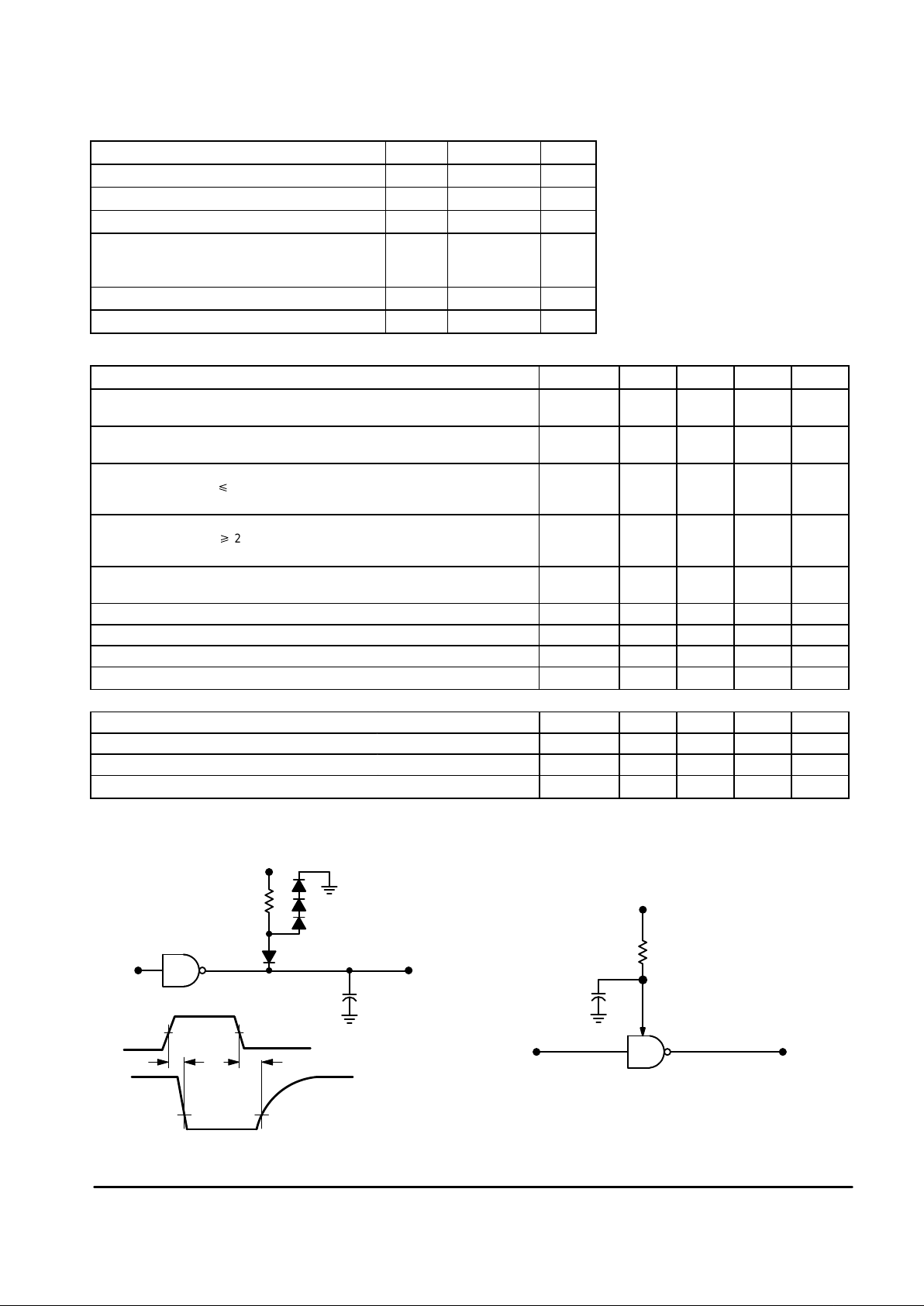
V
in
V
R
All diodes
1N3064
or equivalent
E
o
R
t
TLH
and t
THL
measured
10% – 90%
Figure 1. Switching Response
C
1/4
MC1489A
R
L
5.0 Vdc
50% 50%
3.0 V
E
in
t
THL
CL = 15 pF = total parasitic capacitance which includes
probe and wiring capacitances
1.5 V
1.5 V
t
TLH
t
PLH
Response Node
V
O
E
in
C
L
C, capacitor is for noise filtering.
R, resistor is for threshold shifting.
E
O
Figure 2. Response Control Node
TEST CIRCUITS
 Loading...