MC145402MOTOROLA
1
Advance Information
The MC145402 is a 13–bit linear monotonic digital–to–analog and analog–
to–digital converter implemented in a single silicon–gate CMOS IC. Potential
applications include analog interface for Digital Signal Processor (DSP)
applications, high speed modems, telephone systems, SONAR, Adaptive
Differential Pulse Code Modulation (ADPCM) converters, echo cancellers,
repeaters, voice synthesizers, and music synthesizers.
• 60 dB Signal–to–(Noise Plus Distortion) Ratio Typical
• On–Chip Precision Voltage Reference
• Serial Data Ports
• Two’ s Complement Coding
•± 5 V Supply Operation
• Sample Rates from 100 Hz to 16 kHz (Both A/D and D/A), 100 Hz to
21.3 kHz (A/D Only), and 100 Hz to 64 kHz (D/A Only)
• Input Sample and Hold Provided On–Chip
• 5 V CMOS Inputs; Outputs Capable of Driving Two LSTTL Loads
• Available in a 16–Pin DIP
• Low Power Consumption: 50 mW Typical, 1 mW Power–Down
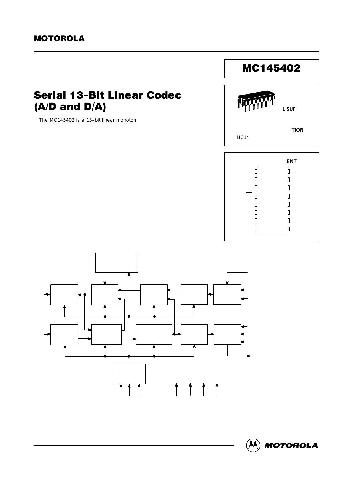
BLOCK DIAGRAM
BANDGAP VOLTAGE
REFERENCE
SAMPLE
AND HOLD
D/A
CONVERTER
DATA
SELECTOR
RECEIVE
LATCH
RECEIVE
SHIFT
REGISTER
15
RDD
13
14
RDC
RCE
2
3
A
out
A
in
7
10
12
11
TDF
TDE
TDC
TDD
65 4 16 8 1 9
VDDVSSVAGV
DG
MSI CCI PDI
SEQUENCE
CONTROLLER
SAMPLE
AND HOLD
COMPARATOR/
OP AMP
SUCCESSIVE
APPROXIMA TION
REGISTER
TRANSMIT
LATCH
TRANSMIT
SHIFT
REGISTER
This document contains information on a new product. Specifications and information herein are subject to change without notice.
Order this document
by MC145402/D
SEMICONDUCTOR TECHNICAL DATA
PIN ASSIGNMENT
L SUFFIX
CERAMIC PACKAGE
CASE 620
ORDERING INFORMATION
MC145402L Ceramic Package
16
1
16
15
14
13
12
11
10
9
V
AG
A
out
A
in
PDI
CCI
MSI
TDF
V
SS
V
DD
RDD
RCE
RDC
TDC
TDE
V
DG
TDD
•
1
2
3
4
5
6
7
8
Motorola, Inc. 1995

MC145402 MOTOROLA
2
ABSOLUTE MAXIMUM RATINGS (Voltages Referenced to V
SS
)
Rating Symbol Value Unit
DC Supply Voltage VDD – V
SS
– 0.5 to 11 V
Voltage, Any Pin to VSS V – 0.5 to VDD + 0.5 V
DC Current Drain per Pin (Excluding
VDD, VSS)
I 10 mA
Operating Temperature Range T
A
– 40 to + 85
°C
Storage Temperature Range T
stg
– 85 to + 150
°C
RECOMMENDED OPERATING CONDITIONS
Parameter Pins
0 to 70°C
Min
25°C
Typ
0 to 70°C
Max
Unit
DC Supply Voltage VDD to V
SS
9.5 10 10.5 V
Power Dissipation, PDI = 1 VDD to V
SS
— 50 80 mW
Power Dissipation, PDI = 0 VDD to V
SS
— 1 5 mW
Conversion Rate Full Cycle A/D and D/A
Short Cycle A/D
Short Cycle D/A
MSI 0.1
0.1
0.1
—
—
—
16
21.3
64
kHz
Conversion Sequence Rate CCI 3.2 — 512 kHz
Data Rate TDC, RDC 16 x f
MSI
— 4096 kHz
Full Scale Analog Levels (Referenced to 600 Ω) AI, AO —
—
3.27
9.5
—
—
Vp
dBm
DIGITAL ELECTRICAL CHARACTERISTICS (V
DD
= 5 V, VSS = – 5 V, VAG = VDG = 0 V, TA = 0 to 70°C)
Characteristic Symbol Min Max Unit
High Level Input Voltage V
IH
3.5 — V
Low Level Input Voltage V
IL
— 1.5 V
Input Current I
in
— ± 1.0 µA
Input Capacitance C
in
— 10 pF
High Level Output Voltage TDD I
out
= – 20 µA
I
out
= – 1 mA
V
OH
4.9
4.3
—
—
V
Low Level Output Voltage TDD I
out
= – 20 µA
I
out
= – 1 mA
V
OL
—
—
0.1
0.4
V
This device contains circuitry to protect the
inputs against damage due to high static
voltages or electrical fields; however, it is
advised that normal precautions be taken to
avoid applications of any voltage higher than
maximum rated voltages to this high impedance circuit. For proper operation it is recommended that Vin and V
out
be constrained to
the range VSS ≤ (Vin or V
out
) ≤ VDD on analog
inputs/outputs and VDG
≤ (V
in
or V
out
) ≤ V
DD
on digital inputs/outputs. Reliability of operation is enhanced if unused digital inputs are tied
to an appropriate logic voltage level (e.g.,
either VDG or VDD) and unused analog Inputs
are tied to VAG.

MC145402MOTOROLA
3
CODER AND DECODER PERFORMANCE (V
DD
= 5 V ± 5%, VSS = – 5 V ± 5%, VAG = VDG = 0 V,
0 dBm0 = 1.60 Vrms = 6.30 dBm (600 Ω), TA = 0 to 70°C, MSI = TDE = RCE = 8 kHz, TDC = RDC = 2.048 MHz, CCI = 256 kHz)
Coder (A/D) Decoder (D/A)
Characteristic
Min Typ Max Min Typ Max
Unit
Resolution 13 — 13 13 — 13 Bits
Conversion Time Full Cycle A/D and D/A
Short Cycle A/D
Short Cycle D/A
62.5
46.9
—
—
—
—
10,000
10,000
—
62.5
—
15.6
—
—
—
10,000
—
10,000
µs
Differential Nonlinearity — — ± 1 — — ± 1 LSB
Gain Error – 0.35 — + 0.35 – 0.35 — + 0.35 dB
Offset – 15
—
—
—
+ 15
—
—
– 20
—
—
—
+ 20
LSB
mV
Idle Channel Noise, 3 kHz Low–Pass — – 75 — — –79 — dBm0
Signal–to–Noise 3.2 dBm0
(Referenced to 1.02 kHz through 0 dBm0
a f
MSI
/2 Low–Pass Filter) – 10 dBm0
– 20 dBm0
– 30 dBm0
– 40 dBm0
– 50 dBm0
—
—
—
—
—
—
—
61
60
57
50
40
30
20
—
—
—
—
—
—
—
—
—
—
—
—
—
—
62
60
59
52
42
32
22
—
—
—
—
—
—
—
dB
ANALOG ELECTRICAL CHARACTERISTICS (V
DD
= 5 V ± 5%, VSS = – 5 V ± 5%, VAG = VDG = 0 V,
0 dBm0 = 1.60 Vrms = 6.30 dBm (600 Ω), TA = 0 to 70°C, MSI = TDE = RCE = 8 kHz, TDC = RDC = 2.048 MHz, CCI = 256 kHz)
Characteristic Pin Symbol Min Typ Max Unit
Input Current AI I
in
— 0.01 ± 1 µA
AC Input Impedance AI Z
in
0.5 — — MΩ
Input Capacitance AI C
in
— — 15 pF
Output Voltage Range AO V
out
– 3.4 — 3.4 V
Power Supply Rejection Ratio
(100 mV RMS on VDD or VSS, 0 – 50 kHz)
AO, TDD PSRR — 40 — dB
Crosstalk, Ain to A
out
and RDD to TDD Referenced to
0 dBm0 @ 1.02 kHz
AO, TDD — — – 90 – 75 dB
Slew Rate AO SR 1.5 3 — V/µs
Settling Time (Full Scale) AO t
settle
— 8 — µs

MC145402 MOTOROLA
4
SWITCHING CHARACTERISTICS
(VDD = + 5 V ± 5%, VSS = – 5 V ± 5%, VAG = VDG = 0 V, TA = 0 to 70°C, CL = 50 pF, See Figure 1)
Characteristic Symbol Min Max Unit
Input Rise Time RCE, RDC, TDC, TDE, CCI, MSI t
r
— 100 ns
Input Fall Time RCE, RDC, TDC, TDE, CCI, MSI t
f
— 100 ns
Output Rise Time TDD t
r
— 80 ns
Output Fall Time TDD t
f
— 80 ns
Pulse Width High RDC, MSI, CCI, TDC, RCE t
wH
100 — ns
Pulse Width Low TDE, MSI, TDC, RCE, RDC t
wL
100 — ns
CCI Pulse Width Low t
wL
500 — ns
MSI Clock Frequency f
MSI
0.1 64 kHz
CCI Clock Frequency f
CCI
3.2 512 kHz
TDC and RDC Clock Frequency f
DC
16 x f
MSI
4.1 MHz
TDC Rising Edge to TDD Data Valid During TDE High t
p1
— 150 ns
TDE Rising Edge to TDD Data Valid During TDC High t
p2
— 150 ns
TDE Rising Edge to TDD Low–Impedance Propagation Delay t
p3
0 100 ns
TDE Falling Edge to TDD High–Impedance Propagation Delay t
p4
— 40 ns
TDE Rising Edge to TDC Falling Edge Setup Time t
su1
t
su2
20
100
—
—
ns
RDC Bit 0 Falling Edge to Last CCI Falling Edge Prior to MSI t
su3
20 — ns
MSI Rising Edge to CCI Falling Edge Setup Time t
su4
t
su5
20
100
—
—
ns
Last CCI Rising Edge (Prior to MSI) to TDE Rising Edge t
su6
100 — ns
Last CCI Rising Edge (Prior to MSI) to First TDC Rising Edge t
su6’
100 — ns
First TDC Falling Edge to Last CCI Rising Edge Prior to MSI t
su7
0 — ns
RCE Rising Edge to RDC Falling Edge Setup Time t
su8
t
su9
20
100
—
—
ns
RDD Valid to RDC Falling Edge Setup T ime t
su10
60 — ns
RDD Hold Time from RDC Falling Edge t
h
100 — ns

MC145402MOTOROLA
5
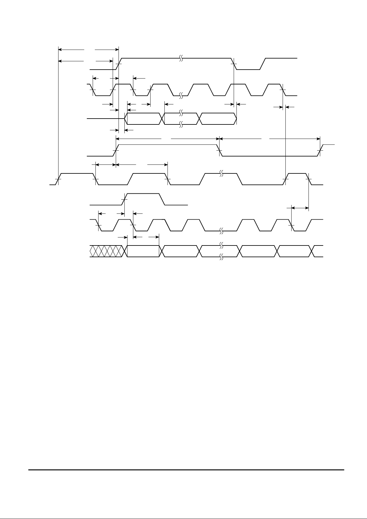
t
su1
TDE
TDC
TDD
MSI
CCI
RCE
RDD
t
su6
t
su2
t
p1
t
p2
t
p1
t
p4
t
su7
t
p3
t
wH
t
wL
t
su4
t
su5
t
su8
t
su9
t
su10
t
h
t
su3
S B11 B10 B1 B0
t
su6
′
CCI
LAST
CCI
LAST
Figure 1. AC Timing Diagram
LAST
BIT
CLOCK
RDC
 Loading...