

MOTOROLA CMOS LOGIC DATA
1
MC14530B
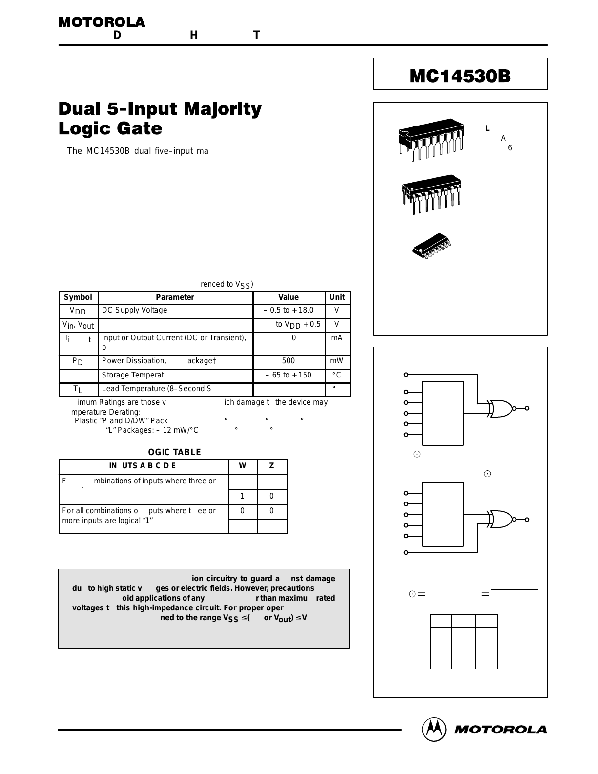
The MC14530B dual five–input majority logic gate is constructed with
P–channel a nd N –channel e nhancement mode d evices i n a single
monolithic structure. Combinational and sequential logic expressions are
easily implemented with the majority logic gate, often resulting in fewer
components than obtainable with the more basic gates. This device can also
provide numerous logic functions by using the W and some of the logic (A
thru E) inputs as control inputs.
• Diode Protection on All Inputs
• Supply Voltage Range = 3.0 Vdc to 18 Vdc
• Capable of Driving Two Low–power TTL Loads or One Low–power
Schottky TTL Load Over the Rated Temperature Range
MAXIMUM RATINGS* (Voltages Referenced to V
SS
)
Symbol
Parameter
Value
Unit
V
DD
DC Supply Voltage
– 0.5 to + 18.0
V
Vin, V
out
Input or Output Voltage (DC or Transient)
– 0.5 to VDD + 0.5
V
Iin, I
out
Input or Output Current (DC or Transient),
per Pin
± 10
mA
P
D
Power Dissipation, per Package†
500
mW
T
stg
Storage Temperature
– 65 to + 150
_
C
T
L
Lead Temperature (8–Second Soldering)
260
_
C
*Maximum Ratings are those values beyond which damage to the device may occur.
†Temperature Derating:
Plastic “P and D/DW” Packages: – 7.0 mW/_C From 65_C To 125_C
Ceramic “L” Packages: – 12 mW/_C From 100_C To 125_C
LOGIC TABLE
INPUTS A B C D E W Z
0 1
more inputs are logical “0”.
1 0
0 0
more inputs are logical “1”.
1 1
This device contains protection circuitry to guard against damage
due to high static voltages or electric fields. However, precautions must
be taken to avoid applications of any voltage higher than maximum rated
voltages to this high-impedance circuit. For proper operation, Vin and
V
out
should be constrained to the range VSS ≤ (Vin or V
out
) ≤ VDD.
Unused inputs must always be tied to an appropriate logic voltage
level (e.g., either VSS or VDD). Unused outputs must be left open.
SEMICONDUCTOR TECHNICAL DATA
Motorola, Inc. 1995
REV 3
1/94
L SUFFIX
CERAMIC
CASE 620
ORDERING INFORMATION
MC14XXXBCP Plastic
MC14XXXBCL Ceramic
MC14XXXBD SOIC
TA = – 55° to 125°C for all packages.
P SUFFIX
PLASTIC
CASE 648
D SUFFIX
SOIC
CASE 751B
BLOCK DIAGRAM
TRUTH TABLE
M5W Z
0 0 1
0 1 0
1 0 0
1 1 1
VDD = PIN 16
VSS = PIN 8
A
W
1
B
C
D
E
2
3
4
5
6
Z
7
M
5
A
B
C
D
E
M
5
13
12
11
10
9
14
W
Z
15
*Z = M5 W = (ABC+ABD+ABE+ACD+
Z = M5 W = (ACE+ADE+BCD+BCE+
Z = M5 W = (BDE+CDE) W
*M5 is a logical “1” if any three or more
inputs are logical “1”.
Exclusive NOR Exclusive OR
For all combinations of inputs where three or
For all combinations of inputs where three or
MOTOROLA CMOS LOGIC DATAMC14530B
2
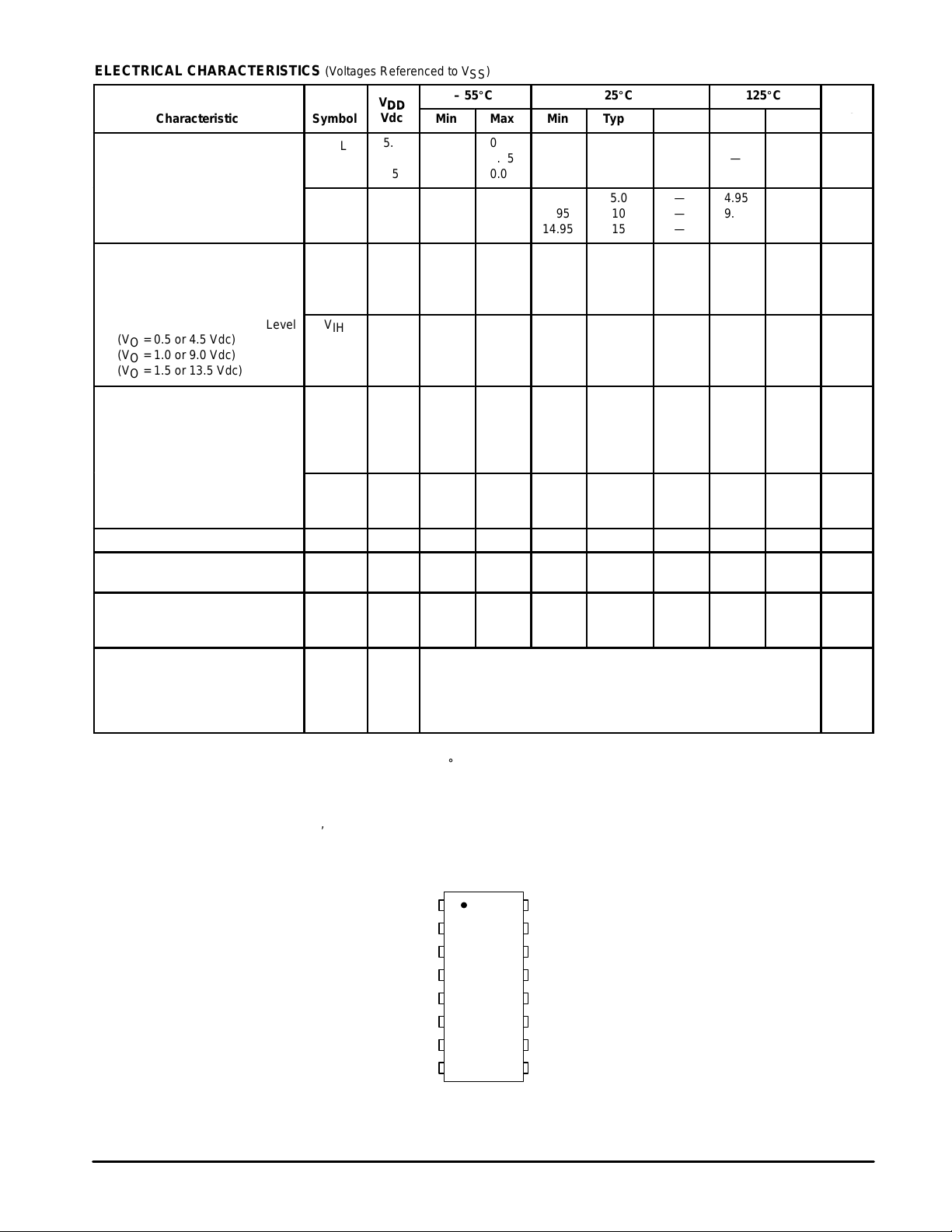
ELECTRICAL CHARACTERISTICS (Voltages Referenced to V
SS
)
V
– 55_C 25_C 125_C
Characteristic
Symbol
V
DD
Vdc
Min Max Min Typ # Max Min Max
Unit
“0” Level
Vin = VDD or 0
V
OL
5.0
10
15
—
—
—
0.05
0.05
0.05
—
—
—
0
0
0
0.05
0.05
0.05
—
—
—
0.05
0.05
0.05
Vdc
“1” Level
Vin = 0 or V
DD
V
OH
5.0
10
15
4.95
9.95
14.95
—
—
—
4.95
9.95
14.95
5.0
10
15
—
—
—
4.95
9.95
14.95
—
—
—
Vdc
“0” Level
(VO = 4.5 or 0.5 Vdc)
(VO = 9.0 or 1.0 Vdc)
(VO = 13.5 or 1.5 Vdc)
V
IL
5.0
10
15
—
—
—
1.2
2.5
3.0
—
—
—
2.25
4.50
6.75
1.25
2.5
3.0
—
—
—
1.15
2.4
2.9
Vdc
“1” Level
(VO = 0.5 or 4.5 Vdc)
(VO = 1.0 or 9.0 Vdc)
(VO = 1.5 or 13.5 Vdc)
V
IH
5.0
10
15
3.85
7.6
12.1
—
—
—
3.75
7.5
12
2.75
5.50
8.25
—
—
—
3.75
7.5
12
—
—
Vdc
I
OH
5.0
5.0
10
15
– 3.0
– 0.64
– 1.6
– 4.2
—
—
—
—
– 2.4
– 0.51
– 1.3
– 3.4
– 4.2
– 0.88
– 2.25
– 8.8
—
—
—
—
– 1.7
– 0.36
– 0.9
– 2.4
—
—
—
—
mAdc
I
OL
5.0
10
15
0.64
1.6
4.2
—
—
—
0.51
1.3
3.4
0.88
2.25
8.8
—
—
—
0.36
0.9
2.4
—
—
—
mAdc
Input Current I
in
15 — ± 0.1 — ±0.00001 ± 0.1 — ± 1.0 µAdc
Input Capacitance
(Vin = 0)
C
in
— — — — 5.0 7.5 — — pF
Quiescent Current
(Per Package)
I
DD
5.0
10
15
—
—
—
0.25
0.5
1.0
—
—
—
0.0005
0.0010
0.0015
0.25
0.5
1.0
—
—
—
7.5
15
30
µAdc
Total Supply Current**†
(Dynamic plus Quiescent,
Per Package)
(CL = 50 pF on all outputs, all
buffers switching)
I
T
5.0
10
15
IT = (0.75 µA/kHz) f + I
DD
IT = (1.50 µA/kHz) f + I
DD
IT = (2.25 µA/kHz) f + I
DD
µAdc
#Data labelled “Typ” is not to be used for design purposes but is intended as an indication of the IC’s potential performance.
**The formulas given are for the typical characteristics only at 25_C.
*To calculate total supply current at loads other than 50 pF:
IT(CL) = IT(50 pF) + (CL – 50) Vfk
where: IT is in µA (per package), CL in pF, V = (VDD – VSS) in volts, f in kHz is input frequency, and k = 0.002.
PIN ASSIGNMENT
13
14
15
16
9
10
11
125
4
3
2
1
8
7
6
D
B
E
B
W
B
Z
B
V
DD
A
B
B
B
C
B
D
A
C
A
B
A
A
A
V
SS
Z
A
W
A
E
A
Output Voltage
Input Voltage
Output Drive Current
(VOH = 2.5 Vdc) Source
(VOH = 4.6 Vdc)
(VOH = 9.5 Vdc)
(VOH = 13.5 Vdc)
(VOL = 0.4 Vdc) Sink
(VOL = 0.5 Vdc)
(VOL = 1.5 Vdc)
MOTOROLA CMOS LOGIC DATA
3
MC14530B
SWITCHING CHARACTERISTICS* (C
L
= 50 pF, TA = 25_C)
Characteristic
Symbol V
DD
Min Typ # Max Unit
Output Rise and Fall Time
t
TLH
, t
THL
= (1.5 ns/pF) CL + 25 ns
t
TLH
, t
THL
= (0.75 ns/pF) CL + 12.5 ns
t
TLH
, t
THL
= (0.55 ns/pF) CL + 9.5 ns
t
TLH
,
t
THL
5.0
10
15
—
—
—
100
50
40
200
100
80
ns
t
PLH
5.0
10
15
—
—
—
375
160
110
960
400
300
ns
t
PHL
5.0
10
15
—
—
—
430
195
120
1200
540
410
ns
t
PLH
5.0
10
15
—
—
—
255
120
86
640
300
210
ns
t
PHL
5.0
10
15
—
—
—
280
125
100
750
330
250
ns
A, B, C, D, E = Gnd; W = Pulse Generator
t
PHL
, t
PLH
= (1.7 ns/pF) CL + 145 ns
t
PHL
, t
PLH
= (0.66 ns/pF) CL + 72 ns
t
PHL
, t
PLH
= (0.5 ns/pF) CL + 50 ns
t
PLH
,
t
PHL
5.0
10
15
—
—
—
230
105
75
575
265
190
ns
*The formulas given are for the typical characteristics only at 25_C.
#Data labelled “Typ” is not to be used for design purposes but is intended as an indication of the IC’s potential performance.
Figure 1. Power Dissipation Test
Circuit and Waveform
A
B
C
D
E
W
A
B
C
D
E
W
PULSE
GENERATOR
V
DD
V
SS
C
L
C
L
Z
Z
8
16
V
DD
V
SS
20 ns 20 ns
V
in
50%
DUTY
CYCLE
Propagation Delay Time
A, C, W = VDD; B, E = Gnd; D = Pulse Generator
t
PLH
t
PLH
t
PLH
t
PHL
t
PHL
t
PHL
A, B, C, D, E = Pulse Generator; W = V
t
PLH
t
PLH
t
PLH
t
PHL
t
PHL
t
PHL
= (1.7 ns/pF) CL + 290 ns
= (0.66 ns/pF) CL + 127 ns
= (0.5 ns/pF) CL + 85 ns
= (1.7 ns/pF) CL + 345 ns
= (0.66 ns/pF) CL + 162 ns
= (0.5 ns/pF) CL + 95 ns
= (1.7 ns/pF) CL + 170 ns
= (0.66 ns/pF) CL + 87 ns
= (0.5 ns/pF) CL + 60 ns
= (1.7 ns/pF) CL + 195 ns
= (0.66 ns/pF) CL + 92 ns
= (0.5 ns/pF) CL + 75 ns
DD
 Loading...