

Motorola MC14528BCL, MC14528BCP, MC14528BD Datasheet
MOTOROLA CMOS LOGIC DATA
1
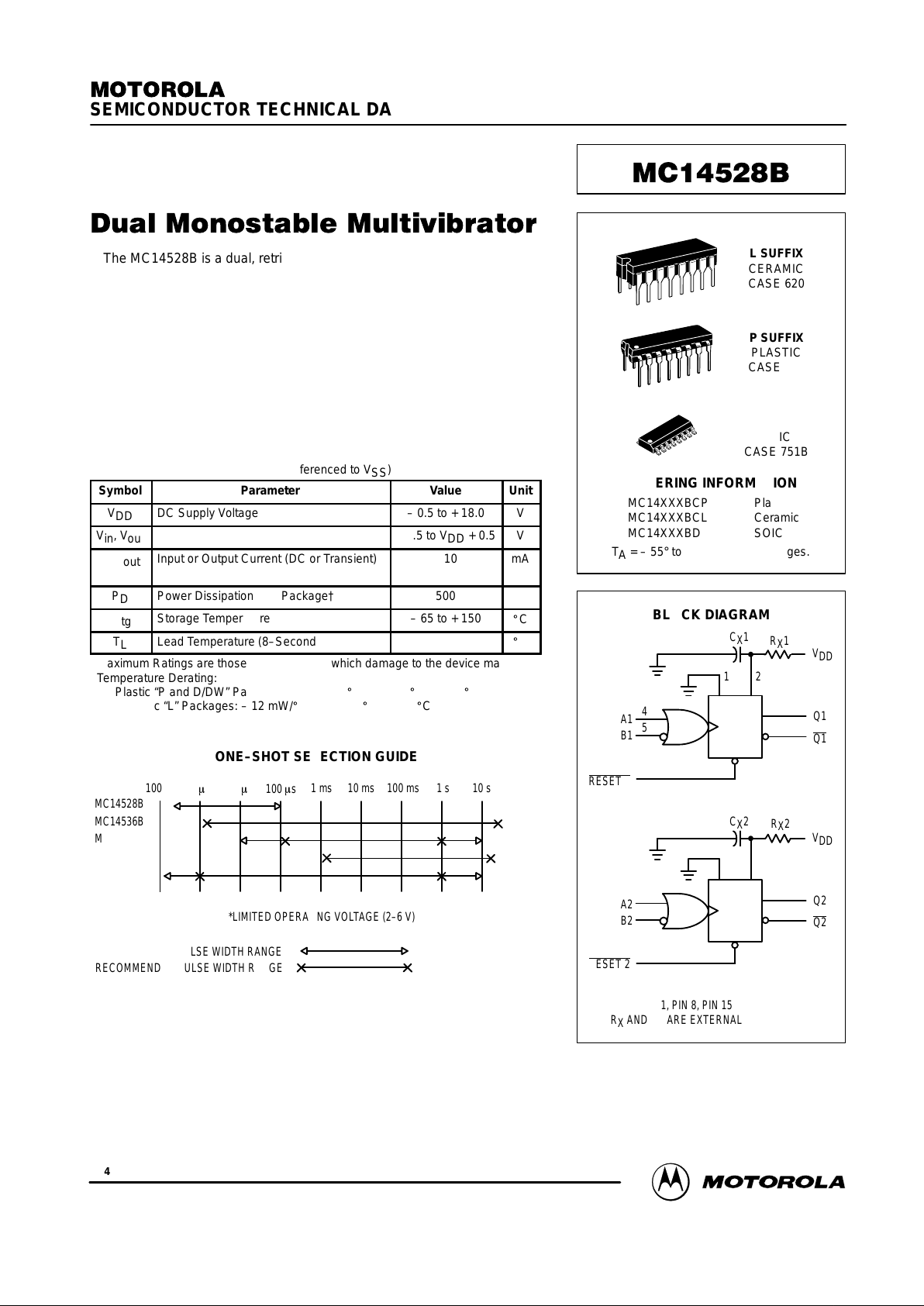
MC14528B
The MC14528B is a dual, retriggerable, resettable monostable multivibrator. It may be triggered from either edge of an input pulse, and produces an
output pulse over a wide range of widths, the duration of which is determined
by the external timing components, CX and RX.
• Separate Reset Available
• Diode Protection on All Inputs
• Triggerable from Leading or Trailing Edge Pulse
• Supply Voltage Range = 3.0 Vdc to 18 Vdc
• Capable of Driving Two Low–power TTL Loads or One Low–power
Schottky TTL Load Over the Rated Temperature Range
• Pin–for–Pin Replacement with the MC14538B
MAXIMUM RATINGS* (Voltages Referenced to V
SS
)
Symbol
Parameter
Value
Unit
V
DD
DC Supply Voltage
– 0.5 to + 18.0
V
Vin, V
out
Input or Output Voltage (DC or Transient)
– 0.5 to VDD + 0.5
V
Iin, I
out
Input or Output Current (DC or Transient),
per Pin
± 10
mA
P
D
Power Dissipation, per Package†
500
mW
T
stg
Storage Temperature
– 65 to + 150
_
C
T
L
Lead Temperature (8–Second Soldering)
260
_
C
*Maximum Ratings are those values beyond which damage to the device may occur.
†Temperature Derating:
Plastic “P and D/DW” Packages: – 7.0 mW/_C From 65_C To 125_C
Ceramic “L” Packages: – 12 mW/_C From 100_C To 125_C
ONE–SHOT SELECTION GUIDE
100 ns
1
m
s 10 ms 100 ms
1 ms 10 ms 100 ms 1 s 10 s
MC14528B
MC14536B
MC14538B
MC14541B
MC4538A*
23 HR
5 MIN.
TOTAL OUTPUT PULSE WIDTH RANGE
RECOMMENDED PULSE WIDTH RANGE
*LIMITED OPERATING VOLTAGE (2–6 V)
SEMICONDUCTOR TECHNICAL DATA
Motorola, Inc. 1995
REV 3
1/94
L SUFFIX
CERAMIC
CASE 620
ORDERING INFORMATION
MC14XXXBCP Plastic
MC14XXXBCL Ceramic
MC14XXXBD SOIC
TA = – 55° to 125°C for all packages.
P SUFFIX
PLASTIC
CASE 648
D SUFFIX
SOIC
CASE 751B
BLOCK DIAGRAM
RESET 1
RESET 2
V
DD
V
DD
Q1
Q1
Q2
Q2
A1
B1
A2
B2
CX1
CX2
RX2
RX1
1 2
4
5
3
6
7
1415
12
11
13
10
9
VDD = PIN 16
VSS = PIN 1, PIN 8, PIN 15
RX AND CX ARE EXTERNAL COMPONENTS
MOTOROLA CMOS LOGIC DATAMC14528B
2
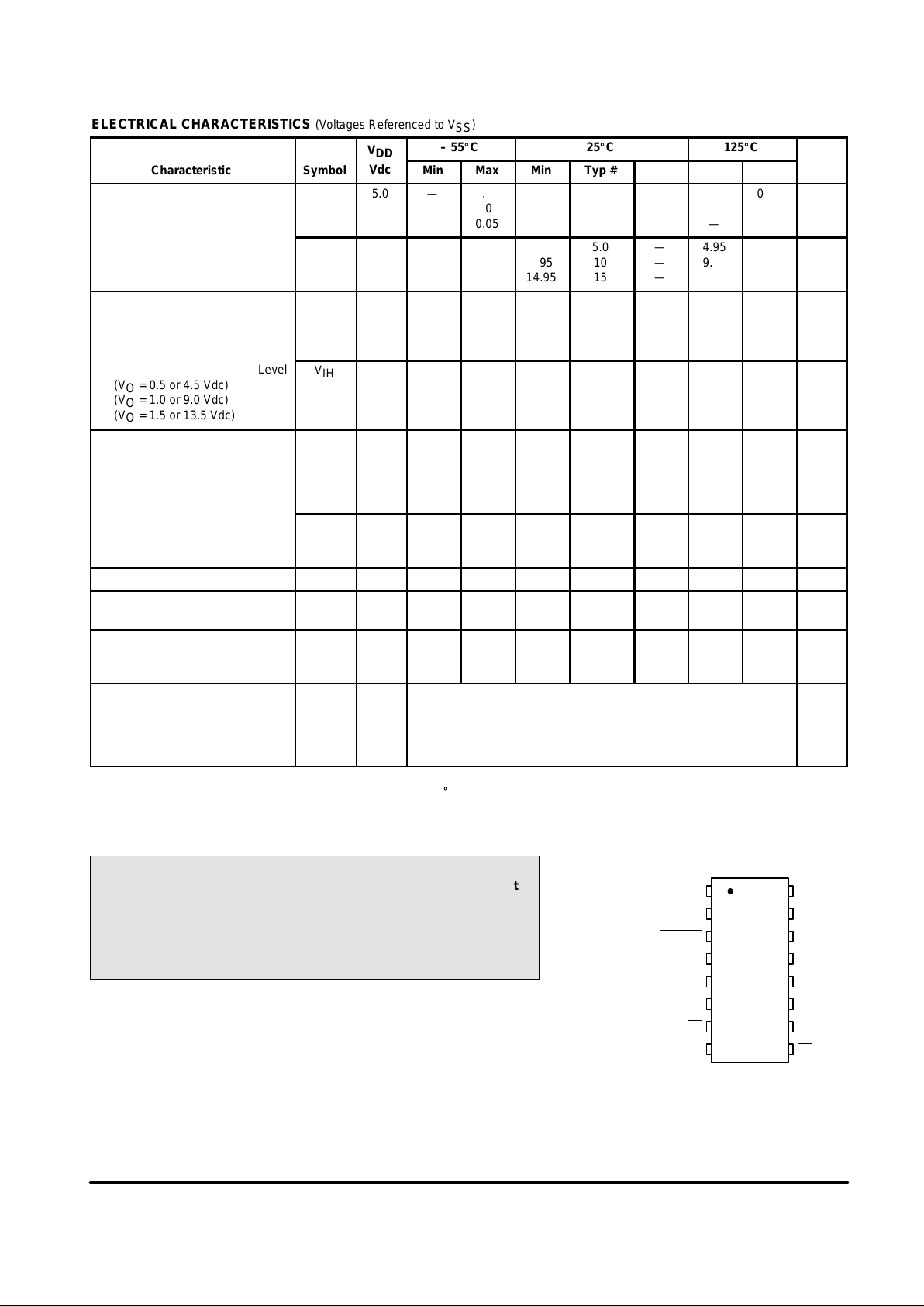
ELECTRICAL CHARACTERISTICS (Voltages Referenced to V
SS
)
V
DD
– 55_C 25_C 125_C
Characteristic
Symbol
DD
Vdc
Min Max Min Typ # Max Min Max
Unit
Output Voltage
“0” Level
Vin = VDD or 0
V
OL
5.0
10
15
—
—
—
0.05
0.05
0.05
—
—
—
0
0
0
0.05
0.05
0.05
—
—
—
0.05
0.05
0.05
Vdc
“1” Level
Vin = 0 or V
DD
V
OH
5.0
10
15
4.95
9.95
14.95
—
—
—
4.95
9.95
14.95
5.0
10
15
—
—
—
4.95
9.95
14.95
—
—
—
Vdc
Input Voltage
“0” Level
(VO = 4.5 or 0.5 Vdc)
(VO = 9.0 or 1.0 Vdc)
(VO = 13.5 or 1.5 Vdc)
V
IL
5.0
10
15
—
—
—
1.5
3.0
4.0
—
—
—
2.25
4.50
6.75
1.5
3.0
4.0
—
—
—
1.5
3.0
4.0
Vdc
“1” Level
(VO = 0.5 or 4.5 Vdc)
(VO = 1.0 or 9.0 Vdc)
(VO = 1.5 or 13.5 Vdc)
V
IH
5.0
10
15
3.5
7.0
11
—
—
—
3.5
7.0
11
2.75
5.50
8.25
—
—
—
3.5
7.0
11
—
—
—
Vdc
Output Drive Current
(VOH = 2.5 Vdc) Source
(VOH = 4.6 Vdc)
(VOH = 9.5 Vdc)
(VOH = 13.5 Vdc)
I
OH
5.0
5.0
10
15
– 1.2
– 0.64
– 1.6
– 4.2
—
—
—
—
– 1.0
– 0.51
– 1.3
– 3.4
– 1.7
– 0.88
– 2.25
– 8.8
—
—
—
—
– 0.7
– 0.36
– 0.9
– 2.4
—
—
—
—
mAdc
(VOL = 0.4 Vdc) Sink
(VOL = 0.5 Vdc)
(VOL = 1.5 Vdc)
I
OL
5.0
10
15
0.64
1.6
4.2
—
—
—
0.51
1.3
3.4
0.88
2.25
8.8
—
—
—
0.36
0.9
2.4
—
—
—
mAdc
Input Current I
in
15 — ± 0.1 — ±0.00001 ± 0.1 — ± 1.0 µAdc
Input Capacitance
(Vin = 0)
C
in
— — — — 5.0 7.5 — — pF
Quiescent Current
(Per Package)
I
DD
5.0
10
15
—
—
—
5.0
10
20
—
—
—
0.005
0.010
0.015
5.0
10
20
—
—
—
150
300
600
µAdc
**Total Supply Current at an
external load Capacitance (CL)
and at external timing
capacitance (CX), use the
formula —
I
T
— IT(CL, CX) = [(CL + 0.36CX)VDDf + 2x10
–8
RXCX(V
DD
–2)2
f] x 10
–3
where: IT in µA (per circuit), CL and CX in pF, RX in megohms,
VDD in Vdc, f in kHz is input frequency.
µAdc
#Data labelled “Typ” is not to be used for design purposes but is intended as an indication of the IC’s potential performance.
** The formulas given are for the typical characteristics only at 25_C.
This device contains protection circuitry to guard against damage
due to high static voltages or electric fields. However, precautions must
be taken to avoid applications of any voltage higher than maximum rated
voltages to this high-impedance circuit. For proper operation, Vin and
V
out
should be constrained to the range VSS ≤ (Vin or V
out
) ≤ VDD.
Unused inputs must always be tied to an appropriate logic voltage
level (e.g., either VSS or VDD). Unused outputs must be left open.
PIN ASSIGNMENT
13
14
15
16
9
10
11
125
4
3
2
1
8
7
6
A2
RESET 2
CX2/RX2
V
SS
V
DD
Q2
Q2
B2
A1
RESET 1
CX1/RX1
V
SS
V
SS
Q1
Q1
B1
MOTOROLA CMOS LOGIC DATA
3
MC14528B
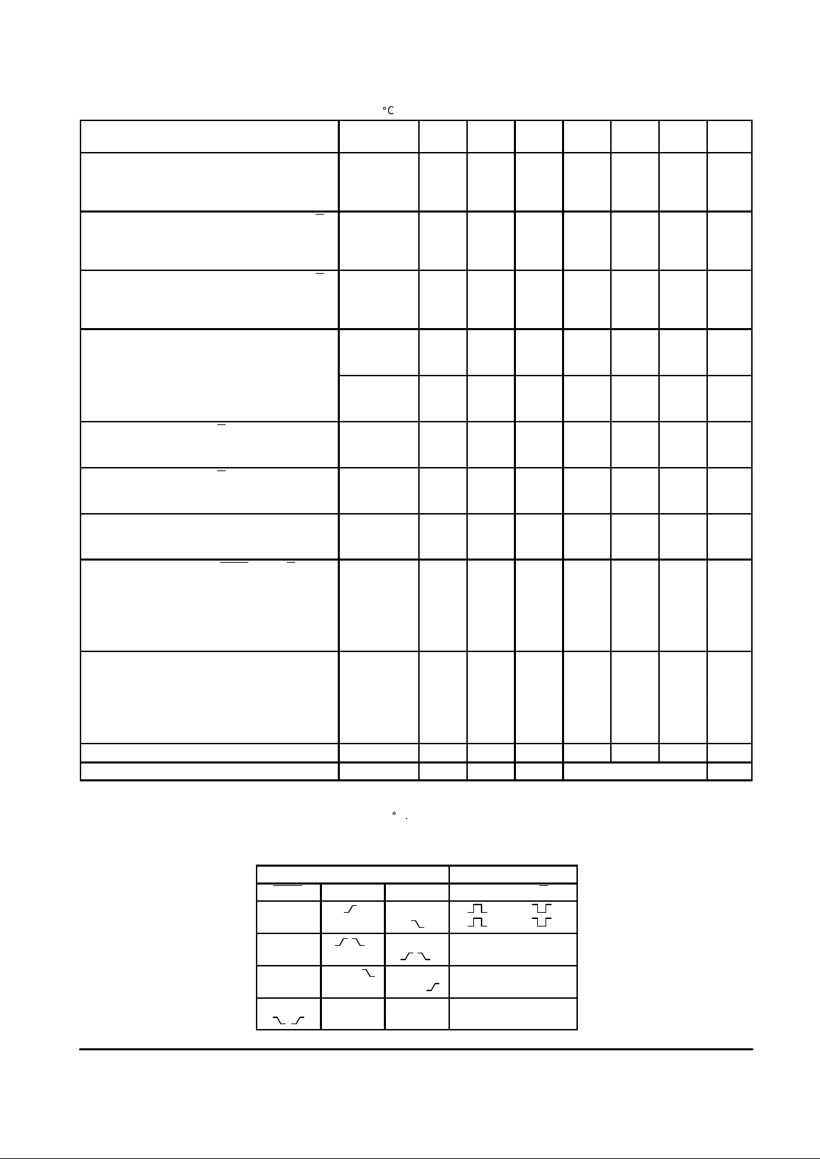
SWITCHING CHARACTERISTICS** (C
L
= 50 pF, TA = 25_C)
Characteristic
Symbol
C
X
pF
R
X
kΩ
V
DD
Vdc
Min Typ # Max Unit
Output Rise and Fall Time
t
TLH
, t
THL
= (1.5 ns/pF) CL + 25 ns
t
TLH
, t
THL
= (0.75 ns/pF) CL + 12.5 ns
t
TLH
, t
THL
= (0.55 ns/pF) CL + 9.5 ns
t
TLH
,
t
THL
— —
5.0
10
15
—
—
—
100
50
40
200
100
80
ns
Turn–Off, Turn–On Delay Time — A or B to Q or Q
t
PLH
, t
PHL
= (1.7 ns/pF) CL + 240 ns
t
PLH
, t
PHL
= (0.66 ns/pF) CL + 87 ns
t
PLH
, t
PHL
= (0.5 ns/pF) CL + 65 ns
t
PLH
,
t
PHL
15 5.0
5.0
10
15
—
—
—
325
120
90
650
240
180
ns
Turn–Off, Turn–On Delay Time — A or B to Q or Q
t
PLH
, t
PHL
= (1.7 ns/pF) CL + 620 ns
t
PLH
, t
PHL
= (0.66 ns/pF) CL + 257 ns
t
PLH
, t
PHL
= (0.5 ns/pF) CL + 185 ns
t
PLH
,
t
PHL
1000 10
5.0
10
15
—
—
—
705
290
210
—
—
—
ns
Input Pulse Width — A or B
t
WH
15 5.0 5.0
10
15
150
75
55
70
30
30
—
—
—
ns
t
WL
1000 10 5.0
10
15
—
—
—
70
30
30
—
—
—
ns
Output Pulse Width — Q or Q
(For CX < 0.01 µF use graph for
appropriate VDD level.)
t
W
15 5.0 5.0
10
15
—
—
—
550
350
300
—
—
—
ns
Output Pulse Width — Q or Q
(For CX > 0.01 µF use formula:
tW = 0.2 RX CX Ln [VDD – VSS])†
t
W
10,000 10 5.0
10
15
15
10
15
30
50
55
45
90
95
µs
Pulse Width Match between Circuits in the same
package
t1 – t2 10,000 10 5.0
10
15
—
—
—
6.0
8.0
8.0
25
35
35
%
Reset Propagation Delay — Reset to Q or Q t
PLH
,
t
PHL
15 5.0 5.0
10
15
—
—
—
325
90
60
600
225
170
ns
1000 10 5.0
10
15
—
—
—
1000
300
250
—
—
—
ns
Retrigger Time t
rr
15 5.0 5.0
10
15
0
0
0
—
—
—
—
—
—
ns
1000 10 5.0
10
15
0
0
0
—
—
—
—
—
—
ns
External Timing Resistance R
X
— — — 5.0 — 1000 kΩ
External Timing Capacitance C
X
— — — No Limits* µF
† RX is in Ohms, CX is in farads, VDD and VSS in volts, PW
out
in seconds.
*If CX > 15 µF, Use Discharge Protection Diode DX, per Fig. 9.
**The formulas given are for the typical characteristics only at 25_C.
#Data labelled “Typ” is not to be used for design purposes but is intended as an indication of the IC’s potential performance.
FUNCTION TABLE
Inputs Outputs
Reset A B Q Q
H H
H L
H L Not Triggered
H H Not Triggered
H L, H, H Not Triggered
H L L, H, Not Triggered
L X X L H
X X Not Triggered
 Loading...