

Motorola MC14527BCP, MC14527BCL, MC14527BDW Datasheet
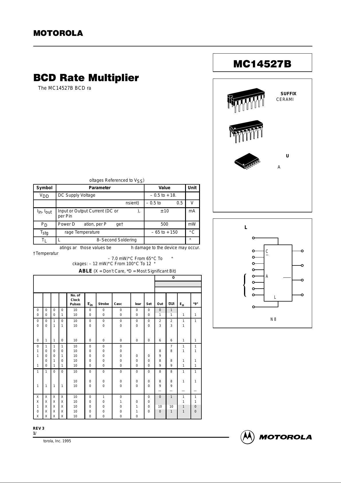
MOTOROLA CMOS LOGIC DATA
1
MC14527B
The MC14527B BCD rate multiplier (DRM) provides an output pulse rate
based upon the BCD input number. For example, if 6 is the BCD input
number, there will be six output pulses for every ten input pulses. This part
may be used for arithmetic operations including multiplication and division.
Typical applications include digital filters, motor speed control and frequency
synthesizers.
• Supply Voltage Range = 3.0 Vdc to 18 Vdc
• Output Clocked on the Negative Going Edge of Clock
• Strobe for Inhibiting or Enabling Outputs
• Enable and Cascade Inputs for Cascade Operation of Two or More
DRMs
• “9” Output for the Parallel Enable Configuration and DRMs in Cascade
• Complementary Outputs
• Clear and Set to Nine Inputs
MAXIMUM RATINGS* (Voltages Referenced to V
SS
)
Symbol
Parameter
Value
Unit
V
DD
DC Supply Voltage
– 0.5 to + 18.0
V
Vin, V
out
Input or Output Voltage (DC or Transient)
– 0.5 to VDD + 0.5
V
Iin, I
out
Input or Output Current (DC or Transient),
per Pin
± 10
mA
P
D
Power Dissipation, per Package†
500
mW
T
stg
Storage Temperature
– 65 to + 150
_
C
T
L
Lead Temperature (8–Second Soldering)
260
_
C
*Maximum Ratings are those values beyond which damage to the device may occur.
†Temperature Derating:
Plastic “P and D/DW” Packages: – 7.0 mW/_C From 65_C To 125_C
Ceramic “L” Packages: – 12 mW/_C From 100_C To 125_C
TRUTH TABLE (X = Don’t Care, *D = Most Significant Bit)
Output
Logic Level
Inputs
Number of Pulses
D* C B A
No. of
Clock
Pulses
EinStrobe Cascade Clear Set Out Out E
out
“9”
0 0 0 0 10 0 0 0 0 0 0 1 1 1
0 0 0 1 10 0 0 0 0 0 1 1 1 1
0 0 1 0 10 0 0 0 0 0 2 2 1 1
0 0 1 1 10 0 0 0 0 0 3 3 1 1
0 1 0 0 10 0 0 0 0 0 4 4 1 1
0 1 0 1 10 0 0 0 0 0 5 5 1 1
0 1 1 0 10 0 0 0 0 0 6 6 1 1
0 1 1 1 10 0 0 0 0 0 7 7 1 1
1 0 0 0 10 0 0 0 0 0 8 8 1 1
1 0 0 1 10 0 0 0 0 0 9 9 1 1
1 0 1 0 10 0 0 0 0 0 8 8 1 1
1 0 1 1 10 0 0 0 0 0 9 9 1 1
1 1 0 0 10 0 0 0 0 0 8 8 1 1
1 1 0 1 10 0 0 0 0 0 9 9 1 1
1 1 1 0 10 0 0 0 0 0 8 8 1 1
1 1 1 1 10 0 0 0 0 0 9 9 1 1
X X X X 10 1 0 0 0 0 — — — —
X X X X 10 0 1 0 0 0 0 1 1 1
X X X X 10 0 0 1 0 0 1 0 1 1
1 X X X 10 0 0 0 1 0 10 10 1 0
0 X X X 10 0 0 0 1 0 0 1 1 0
X X X X 10 0 0 0 0 1 0 1 0 1
SEMICONDUCTOR TECHNICAL DATA
Motorola, Inc. 1995
REV 3
1/94
L SUFFIX
CERAMIC
CASE 620
ORDERING INFORMATION
MC14XXXBCP Plastic
MC14XXXBCL Ceramic
MC14XXXBDW SOIC
TA = – 55° to 125°C for all packages.
P SUFFIX
PLASTIC
CASE 648
DW SUFFIX
SOIC
CASE 751G
BLOCK DIAGRAM
4
12
11
9
10
14
15
2
3
13
7
6
5
1
A
B
C
D
ST
CLOCK
CASC
E
in
S
CLEAR
E
out
OUT
OUT
“9”
MULTIPLIER
RATE INPUT
VDD = PIN 16
VSS = PIN 8
MOTOROLA CMOS LOGIC DATAMC14527B
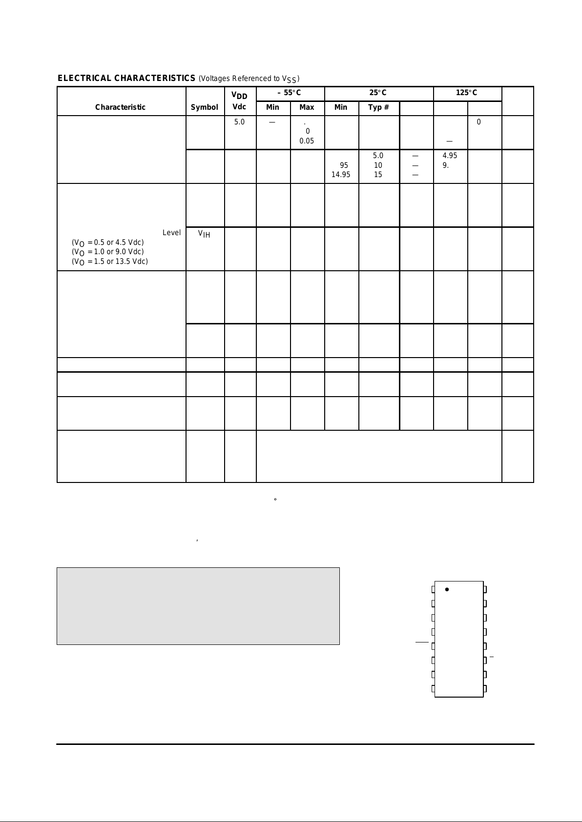
2
ELECTRICAL CHARACTERISTICS (Voltages Referenced to V
SS
)
V
DD
– 55_C 25_C 125_C
Characteristic
Symbol
DD
Vdc
Min Max Min Typ # Max Min Max
Unit
Output Voltage
“0” Level
Vin = VDD or 0
V
OL
5.0
10
15
—
—
—
0.05
0.05
0.05
—
—
—
0
0
0
0.05
0.05
0.05
—
—
—
0.05
0.05
0.05
Vdc
“1” Level
Vin = 0 or V
DD
V
OH
5.0
10
15
4.95
9.95
14.95
—
—
—
4.95
9.95
14.95
5.0
10
15
—
—
—
4.95
9.95
14.95
—
—
—
Vdc
Input Voltage
“0” Level
(VO = 4.5 or 0.5 Vdc)
(VO = 9.0 or 1.0 Vdc)
(VO = 13.5 or 1.5 Vdc)
V
IL
5.0
10
15
—
—
—
1.5
3.0
4.0
—
—
—
2.25
4.50
6.75
1.5
3.0
4.0
—
—
—
1.5
3.0
4.0
Vdc
“1” Level
(VO = 0.5 or 4.5 Vdc)
(VO = 1.0 or 9.0 Vdc)
(VO = 1.5 or 13.5 Vdc)
V
IH
5.0
10
15
3.5
7.0
11
—
—
—
3.5
7.0
11
2.75
5.50
8.25
—
—
—
3.5
7.0
11
—
—
—
Vdc
Output Drive Current
(VOH = 2.5 Vdc) Source
(VOH = 4.6 Vdc)
(VOH = 9.5 Vdc)
(VOH = 13.5 Vdc)
I
OH
5.0
5.0
10
15
– 3.0
– 0.64
– 1.6
– 4.2
—
—
—
—
– 2.4
– 0.51
– 1.3
– 3.4
– 4.2
– 0.88
– 2.25
– 8.8
—
—
—
—
– 1.7
– 0.36
– 0.9
– 2.4
—
—
—
—
mAdc
(VOL = 0.4 Vdc) Sink
(VOL = 0.5 Vdc)
(VOL = 1.5 Vdc)
I
OL
5.0
10
15
0.64
1.6
4.2
—
—
—
0.51
1.3
3.4
0.88
2.25
8.8
—
—
—
0.36
0.9
2.4
—
—
—
mAdc
Input Current I
in
15 — ± 0.1 — ±0.00001 ± 0.1 — ± 1.0 µAdc
Input Capacitance
(Vin = 0)
C
in
— — — — 5.0 7.5 — — pF
Quiescent Current
(Per Package)
I
DD
5.0
10
15
—
—
—
5.0
10
20
—
—
—
0.005
0.010
0.015
5.0
10
20
—
—
—
150
300
600
µAdc
Total Supply Current**†
(Dynamic plus Quiescent,
Per Package)
(CL = 50 pF on all outputs, all
buffers switching)
I
T
5.0
10
15
IT = (0.85 µA/kHz) f + I
DD
IT = (1.75 µA/kHz) f + I
DD
IT = (2.60 µA/kHz) f + I
DD
µAdc
#Data labelled “Typ” is not to be used for design purposes but is intended as an indication of the IC’s potential performance.
**The formulas given are for the typical characteristics only at 25_C.
†To calculate total supply current at loads other than 50 pF:
IT(CL) = IT(50 pF) + (CL – 50) Vfk
where: IT is in µA (per package), CL in pF, V = (VDD – VSS) in volts, f in kHz is input frequency, and k = 0.0012.
This device contains protection circuitry to guard against damage
due to high static voltages or electric fields. However, precautions must
be taken to avoid applications of any voltage higher than maximum rated
voltages to this high-impedance circuit. For proper operation, Vin and
V
out
should be constrained to the range VSS ≤ (Vin or V
out
) ≤ VDD.
Unused inputs must always be tied to an appropriate logic voltage
level (e.g., either VSS or VDD). Unused outputs must be left open.
PIN ASSIGNMENT
13
14
15
16
9
10
11
125
4
3
2
1
8
7
6
CASC
CLEAR
A
B
V
DD
CLOCK
ST
E
in
S
D
C
“9”
V
SS
E
out
OUT
OUT
MOTOROLA CMOS LOGIC DATA
3
MC14527B
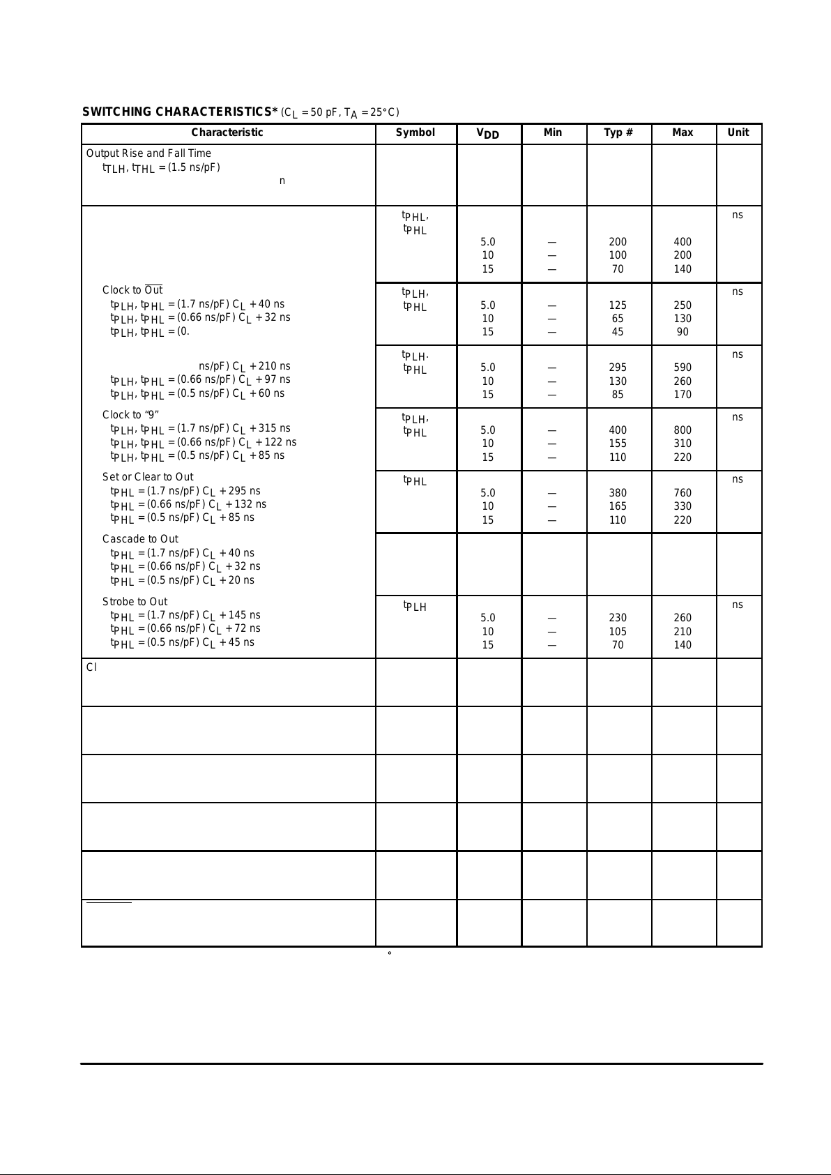
SWITCHING CHARACTERISTICS* (C
L
= 50 pF, TA = 25_C)
Characteristic
Symbol V
DD
Min Typ # Max Unit
Output Rise and Fall Time
t
TLH
, t
THL
= (1.5 ns/pF) CL + 25 ns
t
TLH
, t
THL
= (0.75 ns/pF) CL + 12.5 ns
t
TLH
, t
THL
= (0.55 ns/pF) CL + 9.5 ns
t
TLH
,
t
THL
5.0
10
15
—
—
—
100
50
40
200
100
80
ns
Propagation Delay Time
Clock to Out
t
PLH
, t
PHL
= (1.7 ns/pF) CL + 115 ns
t
PLH
, t
PHL
= (0.66 ns/pF) CL + 67 ns
t
PLH
, t
PHL
= (0.5 ns/pF) CL + 45 ns
t
PHL
,
t
PHL
5.0
10
15
—
—
—
200
100
70
400
200
140
ns
Clock to Out
t
PLH
, t
PHL
= (1.7 ns/pF) CL + 40 ns
t
PLH
, t
PHL
= (0.66 ns/pF) CL + 32 ns
t
PLH
, t
PHL
= (0.5 ns/pF) CL + 20 ns
t
PLH
,
t
PHL
5.0
10
15
—
—
—
125
65
45
250
130
90
ns
t
PLH
, t
PHL
= (1.7 ns/pF) CL + 40 ns
t
PLH
, t
PHL
= (0.66 ns/pF) CL + 32 ns
t
PLH
, t
PHL
= (0.5 ns/pF) CL + 20 ns
Clock to E
out
t
PLH
, t
PHL
= (1.7 ns/pF) CL + 210 ns
t
PLH
, t
PHL
= (0.66 ns/pF) CL + 97 ns
t
PLH
, t
PHL
= (0.5 ns/pF) CL + 60 ns
t
PLH
.
t
PHL
5.0
10
15
—
—
—
295
130
85
590
260
170
ns
t
PLH
, t
PHL
= (1.7 ns/pF) CL + 40 ns
t
PLH
, t
PHL
= (0.66 ns/pF) CL + 32 ns
t
PLH
, t
PHL
= (0.5 ns/pF) CL + 20 ns
Clock to E
out
t
PLH
, t
PHL
= (1.7 ns/pF) CL + 210 ns
t
PLH
, t
PHL
= (0.66 ns/pF) CL + 97 ns
t
PLH
, t
PHL
= (0.5 ns/pF) CL + 60 ns
Clock to “9”
t
PLH
, t
PHL
= (1.7 ns/pF) CL + 315 ns
t
PLH
, t
PHL
= (0.66 ns/pF) CL + 122 ns
t
PLH
, t
PHL
= (0.5 ns/pF) CL + 85 ns
t
PLH
,
t
PHL
5.0
10
15
—
—
—
400
155
110
800
310
220
ns
t
PLH
, t
PHL
= (1.7 ns/pF) CL + 40 ns
t
PLH
, t
PHL
= (0.66 ns/pF) CL + 32 ns
t
PLH
, t
PHL
= (0.5 ns/pF) CL + 20 ns
Clock to E
out
t
PLH
, t
PHL
= (1.7 ns/pF) CL + 210 ns
t
PLH
, t
PHL
= (0.66 ns/pF) CL + 97 ns
t
PLH
, t
PHL
= (0.5 ns/pF) CL + 60 ns
Clock to “9”
t
PLH
, t
PHL
= (1.7 ns/pF) CL + 315 ns
t
PLH
, t
PHL
= (0.66 ns/pF) CL + 122 ns
t
PLH
, t
PHL
= (0.5 ns/pF) CL + 85 ns
Set or Clear to Out
t
PHL
= (1.7 ns/pF) CL + 295 ns
t
PHL
= (0.66 ns/pF) CL + 132 ns
t
PHL
= (0.5 ns/pF) CL + 85 ns
t
PHL
5.0
10
15
—
—
—
380
165
110
760
330
220
ns
t
PLH
, t
PHL
= (1.7 ns/pF) CL + 40 ns
t
PLH
, t
PHL
= (0.66 ns/pF) CL + 32 ns
t
PLH
, t
PHL
= (0.5 ns/pF) CL + 20 ns
Clock to E
out
t
PLH
, t
PHL
= (1.7 ns/pF) CL + 210 ns
t
PLH
, t
PHL
= (0.66 ns/pF) CL + 97 ns
t
PLH
, t
PHL
= (0.5 ns/pF) CL + 60 ns
Clock to “9”
t
PLH
, t
PHL
= (1.7 ns/pF) CL + 315 ns
t
PLH
, t
PHL
= (0.66 ns/pF) CL + 122 ns
t
PLH
, t
PHL
= (0.5 ns/pF) CL + 85 ns
Set or Clear to Out
t
PHL
= (1.7 ns/pF) CL + 295 ns
t
PHL
= (0.66 ns/pF) CL + 132 ns
t
PHL
= (0.5 ns/pF) CL + 85 ns
Cascade to Out
t
PHL
= (1.7 ns/pF) CL + 40 ns
t
PHL
= (0.66 ns/pF) CL + 32 ns
t
PHL
= (0.5 ns/pF) CL + 20 ns
t
PLH
5.0
10
15
—
—
—
125
65
45
250
130
90
ns
t
PLH
, t
PHL
= (1.7 ns/pF) CL + 40 ns
t
PLH
, t
PHL
= (0.66 ns/pF) CL + 32 ns
t
PLH
, t
PHL
= (0.5 ns/pF) CL + 20 ns
Clock to E
out
t
PLH
, t
PHL
= (1.7 ns/pF) CL + 210 ns
t
PLH
, t
PHL
= (0.66 ns/pF) CL + 97 ns
t
PLH
, t
PHL
= (0.5 ns/pF) CL + 60 ns
Clock to “9”
t
PLH
, t
PHL
= (1.7 ns/pF) CL + 315 ns
t
PLH
, t
PHL
= (0.66 ns/pF) CL + 122 ns
t
PLH
, t
PHL
= (0.5 ns/pF) CL + 85 ns
Set or Clear to Out
t
PHL
= (1.7 ns/pF) CL + 295 ns
t
PHL
= (0.66 ns/pF) CL + 132 ns
t
PHL
= (0.5 ns/pF) CL + 85 ns
Cascade to Out
t
PHL
= (1.7 ns/pF) CL + 40 ns
t
PHL
= (0.66 ns/pF) CL + 32 ns
t
PHL
= (0.5 ns/pF) CL + 20 ns
Strobe to Out
t
PHL
= (1.7 ns/pF) CL + 145 ns
t
PHL
= (0.66 ns/pF) CL + 72 ns
t
PHL
= (0.5 ns/pF) CL + 45 ns
t
PLH
5.0
10
15
—
—
—
230
105
70
260
210
140
ns
Clock Pulse Width t
WH
5.0
10
15
500
200
150
250
110
80
—
—
—
ns
Clock Pulse Frequency f
cl
5.0
10
15
—
—
—
2.0
4.5
6.0
1.2
2.5
3.5
MHz
Clock Pulse Rise and Fall Time t
TLH
,
t
THL
5.0
10
15
—
—
—
—
—
—
15
5
4
µs
Set or Clear Pulse Width t
WH
5.0
10
15
240
100
75
80
35
30
—
—
—
ns
Set Removal Time t
rem
5.0
10
15
0
0
0
– 20
– 10
– 7.5
—
—
—
ns
Enable In Setup Time t
su
5.0
10
15
400
150
120
175
60
45
—
—
—
ns
*The formulas given are for the typical characteristics only at 25_C.
#Data labelled “Typ” is not to be used for design purposes but is intended as an indication of the IC’s potential performance.
 Loading...