

Order this document by MC12015/D
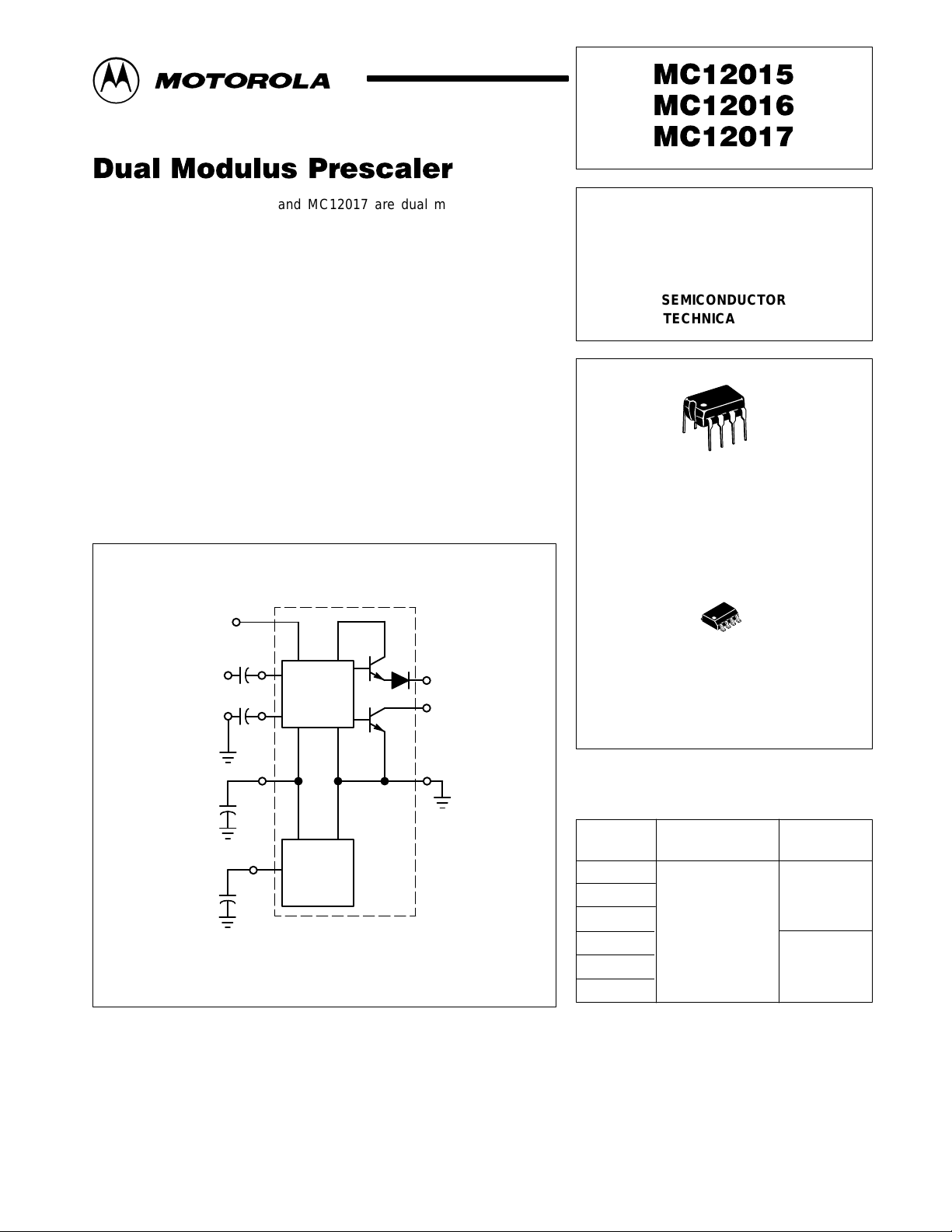
The MC12015, MC12016 and MC12017 are dual modulus prescalers
which will drive divide by 32 and 33, 40 and 41, and 64 and 65, respectively .
An internal regulator is provided to allow these devices to be used over a
wide range of power–supply voltages. The devices may be operated by
applying a supply voltage of 5.0 Vdc ±10% at Pin 7, or by applying an
unregulated voltage source from 5.5Vdc to 9.5 Vdc to Pin 8.
• 225 MHz Toggle Frequency
• Low–Power 7.5 mA Maximum at 6.8 V
• Control Input and Output Are Compatible With Standard CMOS
• Connecting Pins 2 and 3 Allows Driving One TTL Load
• Supply Voltage 4.5 V to 9.5 V
SIMPLIFIED BLOCK DIAGRAM
Control
Input
÷
N / N+1
reg
TO V
2
Active
Pullup
Output
3
Signal
Input
Signal
GND
1
0.001µF
5
6
0.001µF
MECL PLL COMPONENTS
DUAL MODULUS PRESCALER
SEMICONDUCTOR
TECHNICAL DATA
8
1
P SUFFIX
PLASTIC PACKAGE
CASE 626
8
1
D SUFFIX
PLASTIC PACKAGE
CASE 751
(SO–8)
V
reg
7
0.1µF
V
CC
8
0.1µF
1. V
at Pin 7 is not guaranteed to be between 4.5 and
reg
5.5V when VCC is being applied to Pin 8
2. Pin 7 is not to be used as a source of regulated output
voltage
Voltage
Regulator
4
GND
ORDERING INFORMATION
Operating
Device
MC12015D
MC12016D
MC12017D
MC12015P
MC12016P Plastic
MC12017P
Motorola, Inc. 1997 Rev 2
Temperature Range
TA = –40° to +85°C
Package
SO–8
MC12015 MC12016 MC12017
MAXIMUM RATINGS
Regulated Voltage, Pin 7 V
Power Supply Voltage, Pin 8 V
Operating Temperature Range T
Storage Temperature Range T
NOTE: ESD data available upon request.
[tblhead]
Rating Symbol Value Unit
reg
CC
A
stg
8.0 Vdc
10 Vdc
–40 to +85 °C
–65 to +175 °C
ELECTRICAL CHARACTERISTICS (V
Characteristic
Toggle Frequency (Sine Wave Input)
Supply Current I
Control Input HIGH (÷32, 40 or 64) V
Control Input LOW (÷33, 41 or 65) V
Output Voltage HIGH (I
Output Voltage LOW (I
Input Voltage Sensitivity V
35 MHz 400 – 800
50 to 225 MHz 200 – 800
PLL Response Time [Notes 2 and 3] t
NOTES: 1. Pin 2 connected to Pin 3.
2.t
= the period of time the PLL has from the prescaler rising output tranistion (50%) to the modulus control input edge transition
PLL
(50%) to ensure proper modulus selection.
3.t
= period of output waveform.
out
= 50µA) [Nofe 1] V
source
= 2mA) [Note 1] V
sink
= 5.5 to 9.5 V; V
CC
= 4.5 to 5.5 V; TA = –40 to 85°C, unless otherwise noted.)
reg
Symbol Min Typ Max Unit
f
max
f
min
CC
PLL
IH
IL
OH
OL
in
225 – –
– – 35
– 6.0 7.8 mA
2.0 – – V
– – 0.8 V
2.5 – – V
– – 0.5 V
– – t
to 70 ns
out
MHz
mVpp
2
MOTOROLA RF/IF DEVICE DATA
 Loading...