

Motorola MC12009P, MC12011P, MC12013P Datasheet
These devices are two–modulus prescalers which will divide by 5 and
6, 8 and 9, and 10 and 11, respectively. A MECL–to–MTTL translator is
provided to interface directly with the MC12014 Counter Control Logic. In
addition, there is a buffered clock input and MECL bias voltage source.
• MC12009 480 MHz (
550 MHz (B10/11)
• MECL to MTTL Translator on Chip
• MECL and MTTL Enable Inputs
• 5.0 or –5.2 V Operation*
• Buffered Clock Input — Series Input RC Typ, 20 Ohms and 4 pF
• V
Reference Voltage
BB
• 310 Milliwatts (Typ)
B
5/6), MC12011 550 MHz (B8/9), MC12013
Order this document by MC12009/D
MECL PLL COMPONENTS
DUAL MODULUS PRESCALER
SEMICONDUCTOR
TECHNICAL DATA
* When using a 5.0 V supply, apply 5.0 V to Pin 1 (V
(MTTL VCC), Pin 16 (VCC), and ground Pin 8 (VEE). When using
–5.2 V supply, ground Pin 1 (V
Pin 16 (VCC) and apply –5.2 V to Pin 8 (VEE). If the translator is not
required, Pin 6 may be left open to conserve dc power drain.
), Pi n 6 (MTT L VCC), and
CCO
CCO
MAXIMUM RATINGS
Characteristic Symbol Rating Unit
(Ratings above which device life may be impaired)
Power Supply Voltage
(VCC = 0)
Input Voltage
(VCC = 0)
Output Source Current
Continuous
Surge
Storage Temperature Range T
(Recommended Maximum Ratings above which performance may be
degraded)
Operating Temperature Range
MC12009, MC12011, MC12013
DC Fan–Out (Note 1)
(Gates and Flip–Flops)
NOTES: 1. AC fan–out is limited by desired system performance.
2.ESD data available upon request.
V
EE
V
in
I
O
stg
T
A
n 70 —
–8.0 Vdc
0 to V
EE
t
50
t
100
–65 to +175 °C
–30 to +85 °C
), Pi n 6
Vdc
mAdc
16
1
P SUFFIX
PLASTIC PACKAGE
CASE 648
PIN CONNECTIONS
116
V
CCO
Q
2
Q
3
( – )
4
5
( + )
MTTL V
MTTL Output
6
CC
7
8
V
EE
(Top View)
ORDERING INFORMATION
Operating
Device
MC12009P
MC12011P TA = – 35° to +85°C
MC12013P
Temperature Range
15
14
13
12
11
10
9
V
CC
Clock
V
BB
E1 MECL
E2 MECL
E3 MECL
E4 MECL
E5 MECL
Package
Plastic
Motorola, Inc. 1997 Rev 2
MTTL E5
MTTL E4
MECL E3
MECL E2
MECL E1
MC12009 MC12011 MC12013
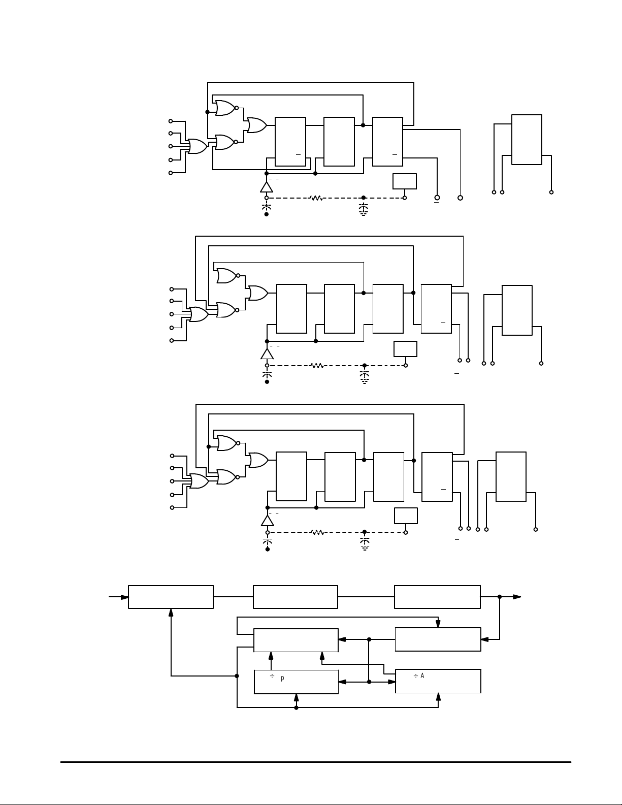
Figure 1. Logic Diagrams
MC12009
9
10
11
12
13
15
Q1
DQ2
C
Q
Recommended Circuitry
For ac coupled Inputs.
1000 pF
Clock Input
1
1 k
MC12011
D
C
D
C
0.1 µF
Q3
Q3
V
BB
14
Q
2
3
Q3
3
MECL
to
MTTL
Trans–
lator
45
–+
7
MTTL
Out
MTTL E5 9
10
MTTL E4
11
MECL E3
12
MECL E2
13
MECL E1
÷ 10 for one or all
E1 thru E5 high
÷ 11 for all
E1 thru E5 low
Tie unused gate inputs low .
MTTL E5 9
10
MTTL E4
11
MECL E3
12
MECL E2
13
MECL E1
Pull–down resistors required on
Pins 2, 3 when not connected
to translator.
Basic IC Capability: ÷ 10/11
Q2
DCQ1 Q3
Recommended Circuitry
For ac coupled Inputs.
15
1000 pF
Clock Input
Q1
D
C
Recommended Circuitry
For ac coupled Inputs.
15
1000 pF
1000 pF
Clock Input
Clock Input
D
C
1 k
MC12013
D
C
1 k
Q2
0.1
0.1
D
C
V
BB
14
µ
F
Q3D
C
V
BB
14
µ
F
Figure 2. T ypical Frequency Synthesizer Application
T oggle
Flip
Flop
C
Toggle
Flop
C
Flip
Q4
Q
Q4
Q
4
4
32
Q
4Q4
Q4Q4
23
54
+–
45
–+
MECL
to
MTTL
Trans–
lator
7
MTTL
Out
MECL
to
MTTL
Trans–
lator
7
MTTL
Out
f
ref
Phase Detector
MC4044
f
out
Low–Pass Filter
Modulus Enable Line
Counter Control Logic
MC12014
B
Np Programmable
Counter MC4016
Counter Reset Line
Zero Detect Line
2
Voltage–Controlled
Oscillator MC1648
MC12009
MC12011
MC12013
B
A Programmable
Counter MC4016
f
out
MOTOROLA RF/IF DEVICE DATA
MC12009 MC12011 MC12013
Under
pp y
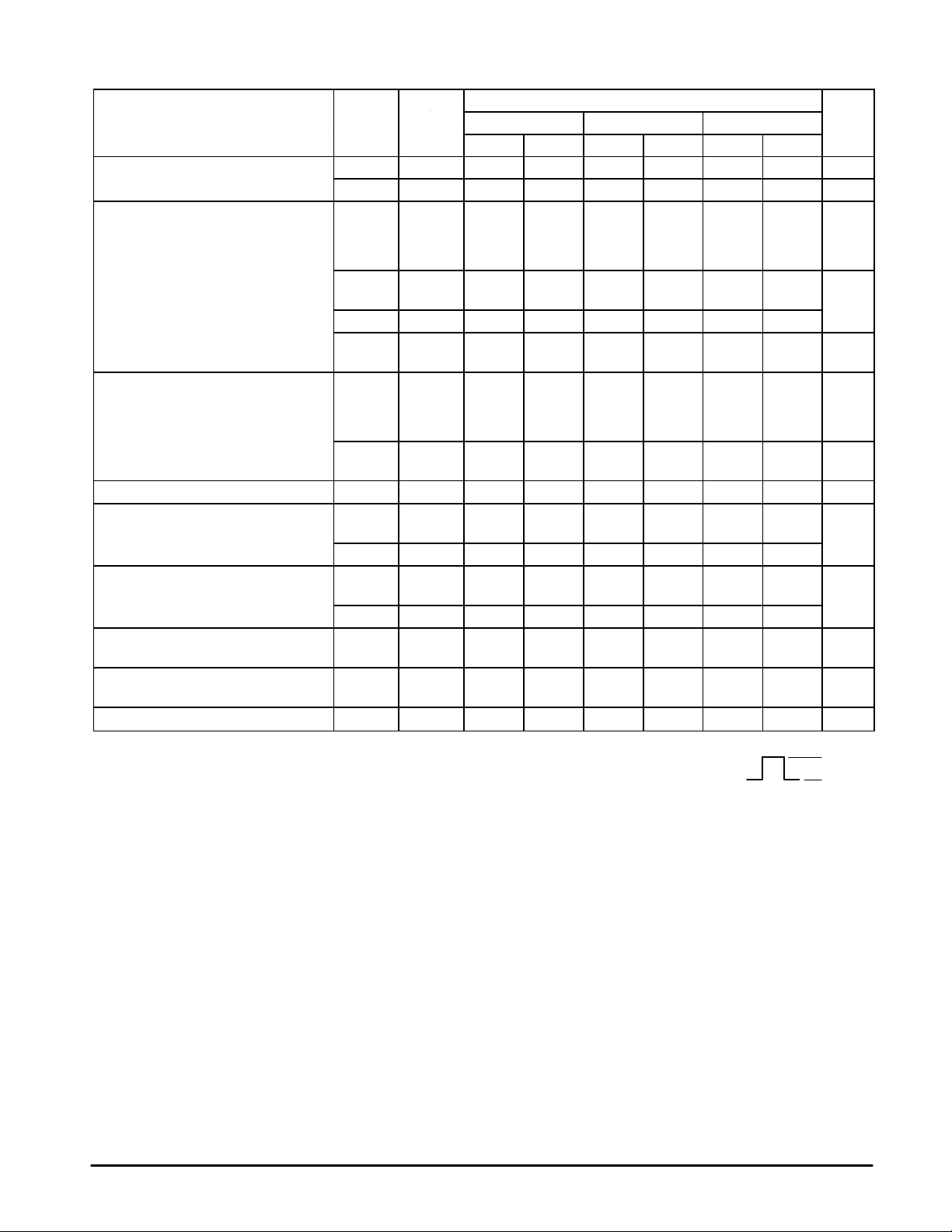
ELECTRICAL CHARACTERISTICS (Supply Voltage = –5.2 V, unless otherwise noted.)
Test Limits
Pin
Characteristic Symbol
Power Supply Drain Current
Input Current I
Leakage Current I
Reference Voltage V
Logic ‘1’ Output Voltage V
Logic ‘0’ Output Voltage V
Logic ‘1’ Threshold Voltage V
Logic ‘0’ Threshold Voltage V
Short Circuit Current I
1. Test outputs of the device must be tested by sequencing through the truth table. All input, power supply and
ground voltages must be maintained between tests. The clock input is the waveform shown.
2. In addition to meeting the output levels specified, the device must divide by 5, 8 or 10 during this test. The clock
input is the waveform shown.
3. In addition to meeting the output levels specified, the device must divide by 6, 9 or 11 during this test. The clock
input is the waveform shown.
I
CC1
I
CC2
inH1
I
inH2
I
inH3
I
inH4
inL1
I
inL2
BB
OH1
(Note 1)
V
OH2
OL1
(Note 1)
V
OL2
OHA
(Note 2)
OLA
(Note 3)
OS
Under
Test
8 –88 –80 –80 mAdc
6 5.2 5.2 5.2 mAdc
15
11
12
13
4
5
5 0.7 3.0 1.0 3.0 1.0 3.6
9
10
15
11
12
13
9
10
14 –1.360 –1.160 Vdc
2
3
7 –2.8 –2.6 –2.4
2
3
7 –4.26 –4.40 –4.48
2
3
2
3
7 –65 –20 –65 –20 –65 –20 mAdc
–30°C +25°C +85°C
Min Max Min Max Min Max
1.7
1.7
–10
–10
–10
–10
–1.6
–1.6
–1.100
–1.100
–1.990
–1.990
–1.120
–1.120
375
375
375
375
6.0
6.0
100
100
–0.890
–0.890
–1.675
–1.675
–1.655
–1.655
2.0
2.0
–10
–10
–10
–10
–1.6
–1.6
–1.000
–1.000
–1.950
–1.950
–1.020
–1.020
250
250
250
250
6.0
6.0
100
100
–0.810
–0.810
–1.650
–1.650
–1.630
–1.630
2.0
2.0
–10
–10
–10
–10
–1.6
–1.6
–0.930
–0.930
–1.925
–1.925
–0.950
–0.950
250
250
250
250
6.4
6.4
100
100
–0.700
–0.700
–1.615
–1.615
–1.595
–1.595
Clock Input
Unit
µAdc
mAdc
µAdc
µAdc
mAdc
Vdc
Vdc
Vdc
Vdc
V
IHmax
V
ILmin
Each MECL 10,000 series circuit has been designed to meet the dc specifications shown in the test table, after thermal equilibrium has been
established. The circuit is in a test socket or mounted on a printed circuit board and transverse air flow greater than 500 linear fpm is maintained.
Outputs are terminated through a 50 Ω resistor to –2.0 V. Test procedures are shown for only one gate. The other gates are tested in the same
manner.
MOTOROLA RF/IF DEVICE DATA
3
MC12009 MC12011 MC12013
Und
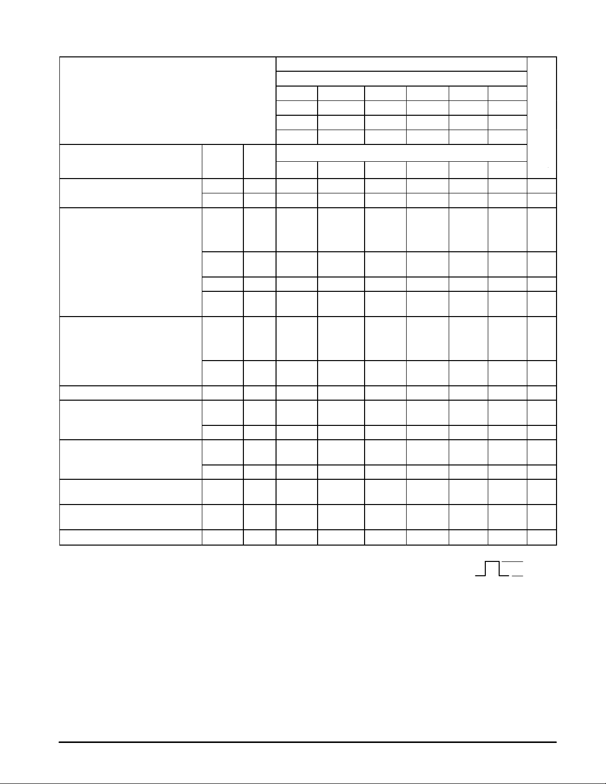
ELECTRICAL CHARACTERISTICS (Supply Voltage = –5.2 V, unless otherwise noted.) (continued)
TEST VOLTAGE/CURRENT VALUES
Volts
@ Test Temperature V
–30°C –0.890 –1.990 –1.205 –1.500 –2.8 –4.7
+25°C –0.810 –1.950 –1.105 –1.475 –2.8 –4.7
+85°C –0.700 –1.925 –1.035 –1.440 –2.8 –4.7
Pin
Characteristic Symbol
Power Supply Drain Current I
Input Current I
Leakage Current I
Reference Voltage V
Logic ‘1’ Output Voltage V
Logic ‘0’ Output Voltage V
Logic ‘1’ Threshold Voltage V
Logic ‘0’ Threshold Voltage V
Short Circuit Current I
1. Test outputs of the device must be tested by sequencing through the truth table. All input, power supply and
ground voltages must be maintained between tests. The clock input is the waveform shown.
2. In addition to meeting the output levels specified, the device must divide by 5, 8 or 10 during this test. The clock
input is the waveform shown.
3. In addition to meeting the output levels specified, the device must divide by 6, 9 or 11 during this test. The clock
input is the waveform shown.
CC1
I
CC2
inH1
I
inH2
I
inH3
I
inH4
inL1
I
inL2
BB
OH1
(Note 1.)23
V
OH2
OL1
(Note 1.)23
V
OL2
OHA
(Note 2.)23
OLA
(Note 3.)23
OS
Test
8 1,16
6 4 5 6
15
11
12
13
4
5
5 4 5 6
9
10
15
11
12
13
9
10
14 1,16
7 5 4 6
7 4 5 6
7 5 4 7 6
IHmax
er
V
IHmax
15
11
12
13
5
5
V
ILmin
TEST VOLTAGE APPLIED TO PINS LISTED BELOW
V
ILmin
4
4
11,12,13
11,12,13
11,12,13
11,12,13
V
IHAminVILAmax
V
IHAminVILAmax
11,12,13
11,12,13
11,12,13
11,12,13
V
IH
V
IH
9
10
Clock Input
V
ILH
V
10
9,10
9,10
9,10
9,10
Gnd
IL
1,16
1,16
1,16
1,16
6
6
1,16
1,16
1,16
1,16
1,16
1,16
9
1,16
1,16
1,16
1,16
1,16
1,16
1,16
1,16
1,16
1,16
V
IHmax
V
ILmin
4
MOTOROLA RF/IF DEVICE DATA

MC12009 MC12011 MC12013
Und
ELECTRICAL CHARACTERISTICS (Supply Voltage = –5.2 V, unless otherwise noted.) (continued)
TEST VOLTAGE/CURRENT VALUES
Volts mA
@ Test Temperature V
–30°C –3.2 –4.4 –5.2 –0.25 16 –0.40
+25°C –3.2 –4.4 –5.2 –0.25 16 –0.40
+85°C –3.2 –4.4 –5.2 –0.25 16 –0.40
Pin
Characteristic Symbol
Power Supply Drain Current I
Input Current I
Leakage Current I
Reference Voltage V
Logic ‘1’ Output Voltage V
Logic ‘0’ Output Voltage V
Logic ‘1’ Threshold Voltage V
Logic ‘0’ Threshold Voltage V
Short Circuit Current I
1. Test outputs of the device must be tested by sequencing through the truth table. All input, power supply and
ground voltages must be maintained between tests. The clock input is the waveform shown.
2. In addition to meeting the output levels specified, the device must divide by 5, 8 or 10 during this test. The clock
input is the waveform shown.
3. In addition to meeting the output levels specified, the device must divide by 6, 9 or 11 during this test. The clock
input is the waveform shown.
CC1
I
CC2
inH1
I
inH2
I
inH3
I
inH4
inL1
I
inL2
BB
OH1
(Note 1.)23
V
OH2
OL1
(Note 1.)23
V
OL2
OHA
(Note 2.)23
OLA
(Note 3.)23
OS
Test
8 8 1,16
6 8 6
15
11
12
13
4
5
5 8 6
9
10
15
11
12
13
9
10
14 8 14 1,16
7 8 7 6
7 8 7 6
7 8 6
IHT
er
V
IHT
9,10
9,10
9,10
9,10
9,10
V
ILT
TEST VOLTAGE APPLIED TO PINS LISTED BELOW
V
ILT
9,10
9,10
V
EE
V
EE
8
8
8
8
8
8
8
8
8,15
8,11
8,12
8,13
8
8
8
8
8
8
8
8
8
8
I
L
I
L
I
OL
I
OL
Clock Input
I
I
OH
OH
Gnd
1,16
1,16
1,16
1,16
1,16
1,16
1,16
1,16
1,16
1,16
1,16
1,16
1,16
1,16
1,16
1,16
1,16
1,16
1,16
1,16
V
IHmax
V
ILmin
6
6
MOTOROLA RF/IF DEVICE DATA
5
 Loading...