

Motorola MC12002P Datasheet
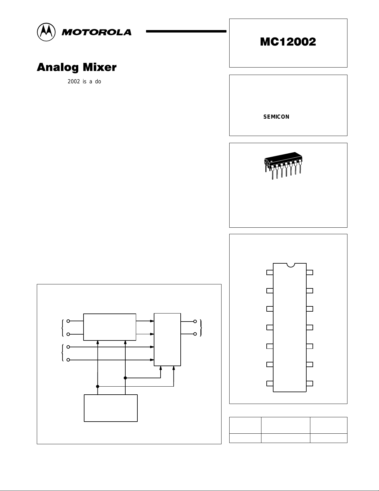
The MC12002 is a double balanced analog mixer, including an input
amplifier feeding the mixer carrier port and a temperature compensated bias
regulator. The input circuits for both the amplifier and mixer are differential
amplifier circuits. The on-chip regulator provides all of the required biasing.
This circuit is designed for use as a balanced mixer in high-frequency
wide-band circuits. Other typical applications include suppressed carrier and
amplitude modulation, synchronous AM detection, FM detection, phase
detection, and frequency doubling, at frequencies up to UHF.
Order this document by MC12002/D
ANALOG MIXER
SEMICONDUCTOR
TECHNICAL DATA
14
1
Local
Oscillator
Inputs
Signal
Inputs
P SUFFIX
PLASTIC PACKAGE
CASE 646
PIN CONNECTIONS
Regulator
Bypass
Local Oscillator
Input
1
2
14 V
13
CC
Resistor Load
Figure 1. Logic Diagram
Local Oscillator
2
3
8
9
Amplifier
V
B
Regulator
Bias
V
R
Carrier
Port
Mixer
Signal
Port
VRV
12
Output
11
B
Alternate Signal
Device
MC12002P TA = –30° to +85°C Plastic
Input
Input
Null Adjust
Null Adjust
V
ORDERING INFORMATION
3
4
5
6
78
EE
Operating
Temperature Range
(Top View)
12
Data Output
11
Data Output
10
Regulator
Bypass
9
Mixer Signal
Input
Mixer Signal
Input
Package
Motorola, Inc. 1997 Rev 5

ELECTRICAL CHARACTERISTICS
Under
Pin
Under
CC
inH
I
inL
IO
IO
I
out
Bias
A
Test
14 — — — 16 — — mAdc — — 11,12,14 5,6,7
1112————0.7
1
1112————2.1
2
11
11
12
12
11,12
1
11,12
2
10
11 — — 5.0 — — — V/V 2 11 9 14 7
V
11 — — 0.28 — — — V/V 8 11 3 14 7
Characteristic Symbol
Power Supply Drain I
Input Current
Output Current
Differential Current ∆IO
Bias Voltage V
AC Gain (See Figure 1)
(Frequency =
100 MHz) *Note
NOTE: *Note: AC Gain is a function of collector load impedance.
I
∆IO
–30°C +25°C +85°C
Min Max Min Max Min Max Unit
2
—
—
—
—
—
—
—
—
—
—
—
—
–100
–200
2.33
390
275
275
1.26
—
—
—
—
—
—
—
—
—
—
—
—
+100
+200
2.53
590
415
415
1.46
3
8
9
2
3
8
9
1
4
5
6
MC12002
Test Limits
—
—
—
—
– 0.7
– 0.7
– 0.7
– 0.7
0.7
2.1
4.2
4.2
4.2
4.2
–100
–200
2.32
400
285
285
1.185
1.385
0.75
0.75
0.75
0.75
+100
+200
2.52
600
425
425
—
—
—
—
—
—
—
—
—
—
—
—
1.3
1.3————
3.9
3.9————
7.8
— —
7.8
7.8
7.8
–100
–200
2.3
410
295
295
1.105
—
—
—
—
—
—
—
—
—
—
—
+100
+200
2.5
610
435
435
1.305
TEST VOLTAGE VALUES
V
IHmaxVILminVCC
+2.9 +2.0 +5.0
VOLTAGE APPLIED TO PINS
LISTED BELOW
V
IHmaxVILminVCC
mAdc
mAdc
mAdc
mAdc
mAdc
mAdc
mAdc
mAdc
mAdc
mAdc
mAdc
mAdc
mAdc
mAdc
mAdc
mAdc
µAdc
µAdc
Vdc
mVdc
mVdc
mVdc
Vdc
2
3
8
9
—
—
—
—
—
—
—
—
2,9
3,8
2,8
3,9
—
—
—
—
—
—
—
PulseInPulse
Out
Volts
—
11,12,14
—
11,12,14
—
11,12,14
—
11,12,14
2
11,12,14
3
11,12,14
8
11,12,14
9
11,12,14
——11,12,14
11,12,1477
——11,12,14
11,12,14
—
11,12,14
—
11,12,14
—
11,12,14
—
11,12,14
——11,12,14
11,12,1475,6,7
—
11,12,14
—
11,12,14
—
11,12,14
—
11,12,14
—
11,12,14
–3.0 V Gnd V
Gnd
5,6,7
5,6,7
5,6,7
5,6,7
5,6,7
5,6,7
5,6,7
5,6,7
5,6,7
5,6,7
5,6,7
5,6,7
5,6,7
5,6,7
5,6,7
5,6,7
7
7
5,6,7
EE
2
MOTOROLA RF/IF DEVICE DATA
MC12002
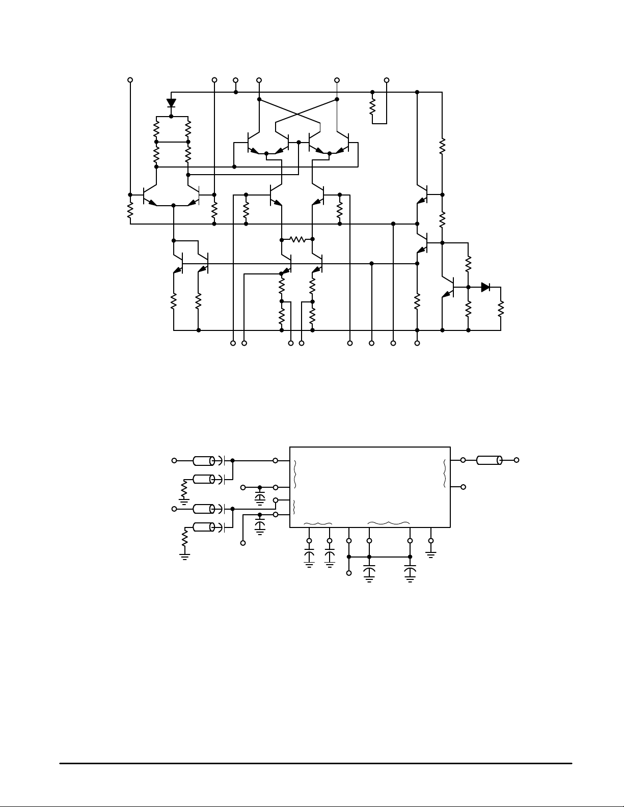
Figure 2. Analog Mixer Circuit Schematic
1 k
2
6767
67 67
167167
1 k
1 k1 k
100
167 167
333333
12
133
1095648
1311143
663
17
493
318
880
350631
0.1
µ
f
Signal A
50
Signal B
50
Note 1:
VIL= –3.0 V on pin 3 when pin 8 is under test.
VIL= –3.0 V on pin 9 when pin 2 is under test.
Signal A = 30 mVpp
Signal B = 300 mVpp
Freq. = 100 MHz
0.1
0.1
0.1
µ
f
Note 1
µ
f
µ
F
0.1
µ
Note 1
Figure 3. AC Gain Test
2
Local Oscillator
Inputs
3
8
f
0.1
9
µ
f
0.1
Mixer
Inputs
Reg. Bypass
µ
F
V
0.1
µ
F
–5.0V
EE
12
Outputs
Null
Adj.
57110
614
10
11
V
CC
µ
F0.1µf
All input and output
cables to the scope are
equal lengths of 50-ohm
coaxial cable.
The unused output is
connected to a 50-ohm
resistor to ground.
MOTOROLA RF/IF DEVICE DATA
3
 Loading...