

MOTOROLA MC1121DMR2 Datasheet
MC1121
100mA Charge Pump V oltage
Converter with Shutdown
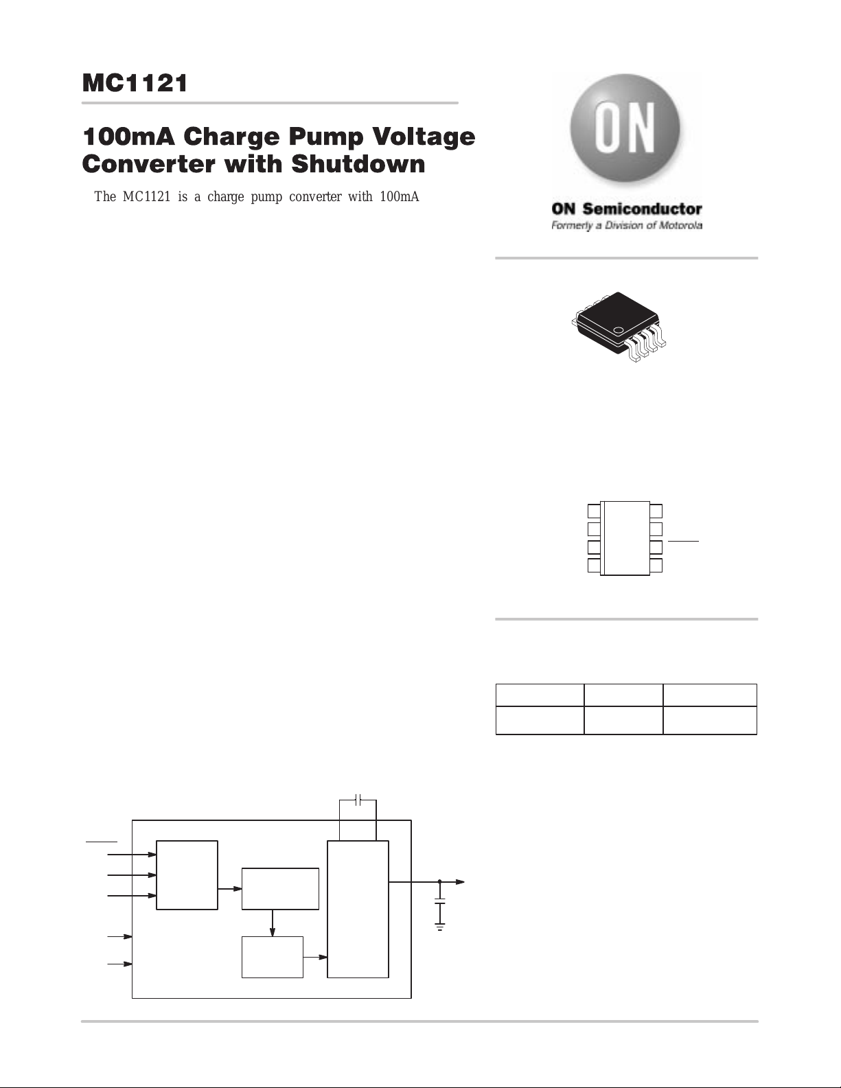
The MC1121 is a charge pump converter with 100mA output
current capability. It converts a 2.4V to 5.5V input to a corresponding
negative output voltage. As with all charge pump converters, the
MC1121 uses no inductors saving cost, size, and reducing EMI.
An on–board oscillator operates at a typical frequency of 10kHz (at
VDD = 5V) when the frequency control input (FC) is connected to
ground. The oscillator frequency increases to 200kHz when FC is
connected to VDD, allowing the use of smaller capacitors. Operation at
sub–10kHz frequencies results in lower quiescent current and is
accomplished with the addition of an external capacitor from OSC (pin
7) to ground. The MC1121 can be driven from an external clock
connected OSC. Typical supply current at 10kHz is 50µA, and falls to
less than 1µA when the shutdown input is brought low, whether the
internal or an external clock is used. The MC1121 is available in a
Micro–8 package.
http://onsemi.com
Micro8
DM SUFFIX
CASE TBD
PRELIMINARY INFORMATION
Features
• Converts a 2.4V to 5.5V Input Voltage to a Corresponding Negative
Output Voltage (Inverter Mode)
• Uses Only 2 Capacitors; No Inductors Required!
• High Output Current: 100mA
• Selectable Oscillator Frequency: 10kHz to 200kHz
• Power–Saving Shutdown Input
• Optional High–Frequency Operation Allows Use of Small Capacitors
• Low Operating Current (FC = GND): 50µA
• T ested Operating Temperature Range: –40°C to +85°C
Typical Applications
• Laptop Computers
• Medical Instruments
• Disk Drives
• µP–Based Controllers
• Process Instrumentation
FUNCTIONAL BLOCK DIAGRAM
+
–
CAP
–
V
out
C2
+
SHDN
FC
OSC
V
DD
GND
OSC
CONTROL
MC1121
CAP
RC
OSCILLATOR
LOGIC
CIRCUITS
+
C1
SWITCH
MATRIX
PIN CONFIGURATION
(Top View)
FC
1
CAP+
2
3
4
MC1121
GND
CAP–
ORDERING INFORMATION
Device Package Shipping
MC1121DMR2 Micro–8 2500 Tape/Reel
8
7
6
5
V
DD
OSC
SHDN
V
OUT
Semiconductor Components Industries, LLC, 1999
February , 2000 – Rev. 0
1 Publication Order Number:
MC1121/D
MC1121
Á
ББББББ
Á
Á
Á
ББББББ
ББББББ
ББББББ
ББББББ
ББББББ
ББББББ
ББББББ
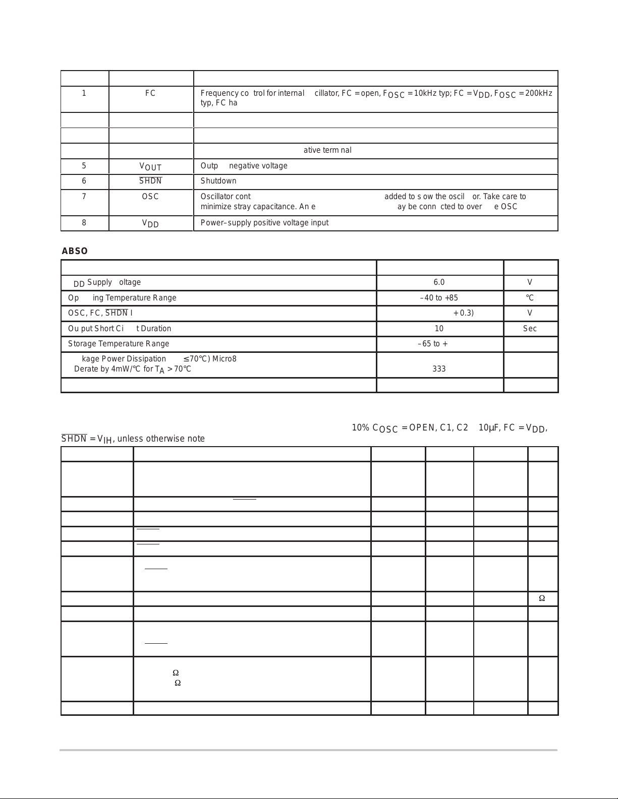
PIN DESCRIPTION
Pin No. Symbol Description
1
ÁÁÁ
2
3
4
5
6
7
8
ABSOLUTE MAXIMUM RATINGS*
VDD Supply Voltage 6.0 V
Operating Temperature Range –40 to +85 °C
OSC, FC, SHDN Input Voltage –0.3 to (VDD + 0.3) V
Output Short Circuit Duration 10 Sec
Storage Temperature Range –65 to +150 °C
Package Power Dissipation (TA ≤ 70°C) Micro8
Derate by 4mW/°C for TA > 70°C
Lead Temperature (Soldering, 10 Seconds) +300 °C
* Maximum Ratings are those values beyond which damage to the device may occur.
FC
ÁÁÁÁ
CAP+
GND
CAP–
V
OUT
SHDN
OSC
V
DD
Frequency control for internal oscillator, FC = open, F
typ, FC has no effect when OSC pin is driven externally
ББББББББББББББББББББББ
= 10kHz typ; FC = VDD, F
OSC
OSC
Charge–pump capacitor, positive terminal
Power–supply ground input
Charge–pump capacitor, negative terminal
Output, negative voltage
Shutdown
Oscillator control input. An external capacitor can be added to slow the oscillator. Take care to
minimize stray capacitance. An external oscillator also may be connected to overdrive OSC
Power–supply positive voltage input
Parameter Value Unit
333
= 200kHz
mW
ELECTRICAL CHARACTERISTICS (TA = –40°C to +85°C, VDD = 5V ±10% C
= OPEN, C1, C2 = 10µF, FC = VDD,
OSC
SHDN = VIH, unless otherwise noted. Typical values are at TA = 25°C.)
Symbol Characteristic Min Typ Max Unit
I
DD
I
DD(SHDN)
V
DD
V
IH
V
IL
I
IN
R
OUT
I
OUT
F
OSC
P
EFF
V
EFF
Active Supply Current
RL = Open, FC = Open or GND
RL = Open, FC = V
DD
—
—
50
0.6
100
1.0
Shutdown Supply Current (SHDN = 0V) — 0.2 1.0 µA
Supply Voltage 2.4 — 5.5 V
SHDN Logic High Input Voltage VDD x 0.8 — — V
SHDN Logic Low Input Voltage — — 0.4 V
Input Leakage Current
SHDN
, OSC
FC Pin
Output Source Resistance (I
Output Current (V
more negative than –3.75V) 60 100 — mA
OUT
–1.0
–4.0
= 60 mA) — 12 20
OUT
—
—
1.0
4.0
Oscillator Frequency
OSC Open, FC = Open or GND
= VIH, FC = V
SHDN
DD
5.0
100
10
200
—
—
Power Efficiency (FC = GND)
RL = 2kW between VDD and V
RL = 1 kW between V
IL = 60 mA to GND
OUT
and GND
OUT
93
94
—
97
97
92
—
—
—
Voltage Conversion Efficiency (RL = OPEN) 99 99.9 — %
µA
mA
µA
W
kHz
%
http://onsemi.com
2
MC1121
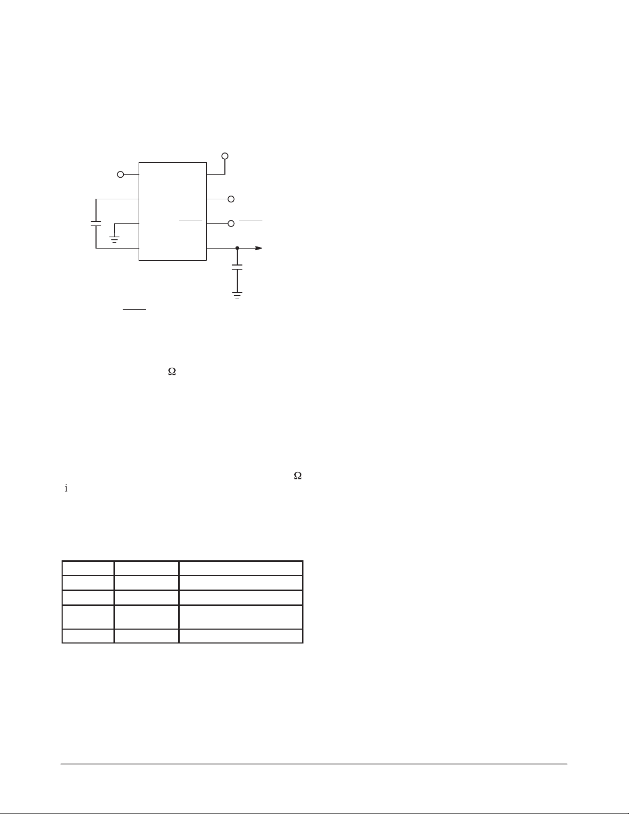
APPLICATIONS INFORMATION
Negative Voltage Converter
The MC1121 is typically used as a charge–pump voltage
inverter. C1 and C2 are the only two external capacitors used
in the operating circuit (see Figure 1).
2.4 V to 5.5 V
MC1121
+
SHDN
–
V
DD
OSC
V
out
7
SHDN*
6
V
5
–
+
out
C2
+
C2
–
NOTES: *SHDN
Figure 1. Charge Pump Inverter
FC
18
CAP
2
GND
3
CAP
4
should be tied to VDD if not used.
The MC1121 is not actively regulated. A typical output
source resistance of 11.8W means that an input of +5V
results in - 5V output voltage under light load, and only
decreases to - 3.8V (typ) with a 100mA load.
The supplied output current is from capacitor C2 during
one–half the charge–pump cycle. This results in a
peak–to–peak ripple of:
V
RIPPLE
Where f
= I
is 5kHz (one half the nominal 10kHz
PUMP
OUT
/2(f
PUMP
) (C2) + I
OUT
(ESRC2)
oscillator frequency), and C2 = 150µF with an ESR of 0.2
ripple is about 90mV with a 100mA load current. If C2 is
raised to 390µF, the ripple drops to 45mV.
Changing Oscillator Frequency
The MC1121’s clock frequency is controlled by four
modes:
The oscillator runs at 10kHz (typical) when FC and OSC
are not connected. The oscillator frequency is lowered by
connecting a capacitor between OSC and GND, but FC can
still multiply the frequency by 20 times in this mode.
An external clock source that swings within 100mV of
VDD and GND may overdrive OSC in the inverter mode.
OSC can be driven by any CMOS logic output. When OSC
is overdriven, FC has no effect.
Note that the frequency of the signal appearing at CAP
+
and CAP- is half that of the oscillator. In addition, by
lowering the oscillator frequency, the effective output
resistance of the charge–pump increases. T o compensate for
this, the value of the charge–pump capacitors may be
increased.
Because the 5kHz output ripple frequency may be low
enough to interfere with other circuitry, the oscillator
frequency can be increased with the use of the FC pin or an
external oscillator. The output ripple frequency is half the
selected oscillator frequency. Although the MC1121’s
quiescent current will increase if the clock frequency is
increased, it allows smaller capacitance values to be used for
C1 and C2.
Capacitor Selection
In addition to load current, the following factors affect the
MC1121 output voltage drop from its ideal value 1) output
resistance, 2) pump (C1) and reservoir (C2) capacitor ESRs,
and 3) C1 and C2 capacitance.
The voltage drop is the load current times the output
resistance. The loss in C2 is the load current times C2’ s ESR;
C1’s loss is larger because it handles currents greater than
the load current during charge–pump operation. Therefore,
W
the voltage drop due to C1 is about four times C1’s ESR
multiplied by the load current, and a low (or high) ESR
capacitor has a greater impact on performance for C1 than
for C2.
In general, as the MC1121’s pump frequency increases,
capacitance values needed to maintain comparable ripple
and output resistance diminish proportionately.
FC OSC Oscillator Frequency
Open Open 10kHz
FC = V
Open or
FC = V
Open External Clock External Clock Frequency
Open 200kHz
DD
External
Capacitor
DD
Reduced from 10kHz or
200kHz depending on FC state
Cascading Devices
To produce greater negative magnitudes of the initial
supply voltage, the MC1121 may be cascaded (see Figure 2).
The resulting output resistance is approximately equal to the
sum of individual MC1121 R
(where n is an integer representing the number of devices
cascaded) is defined by
V
OUT
http://onsemi.com
3
= - n (VIN).
values. The output voltage
OUT
 Loading...