

MOTOROLA MC10SX1190DT, MC10SX1190DTR2 Datasheet
MC10SX1190
Product Preview
Fibre Channel Coaxial
Cable Driver and Loop
Resiliency Circuit
The MC10SX1190 is a differential receiver, differential transmitter
specifically designed to drive coaxial cables. It incorporates the output
cable drive capability of the MC10EP89 Coaxial Cable Driver with
additional circuitry to multiplex the output cable drive source between
the cable receiver or the local transmitter inputs. The multiplexer
control circuitry is TTL compatible for ease of operation.
The MC10SX1190 is useful as a bypass element for Fibre
Channel-Arbitrated Loop (FC-AL) or Serial Storage Architecture
(SSA) applications, to create loop style interconnects with fault
tolerant, active switches at each device node. This device is
particularly useful for back panel applications where small size is
desirable.
The EP89 style drive circuitry produces swings approximately 70%
larger than a standard PECL output. When driving a coaxial cable,
proper termination is required at both ends of the line to minimize
reflections. The 1.4V output swings allow for proper termination at
both ends of the cable, while maintaining the required swing at the
receiving end of the cable. Because of the larger output swings, the
QT, QT
VCC– 3.0V instead of 50Ω to VCC– 2.0V.
• 2.5 Gbps Operation
• 425ps Propagation Delay
• 1.4V Output Swing on the Cable Driving Output
• PECL Mode: 3.0V to 5.5V V
• ECL Mode: 0V V
• 75kΩ Internal Input Pull Down Resistors
• >1000 Volt ESD Protection
outputs are terminated into the thevenin equivalent of 50Ω to
, with VEE = 0V
CC
, with VEE = –3.0V to –5.5V
CC
V
V
V
CC
QR QR
CC
1920 18 17 16 15 14
EE
DT DT V
13
CC
VBBV
12911
EE
http://onsemi.com
20
1
TSSOP–20
DT SUFFIX
CASE 948E
MARKING DIAGRAM
10SX
1190
ALYW
*For additional information, see Application Note
AND8002/D
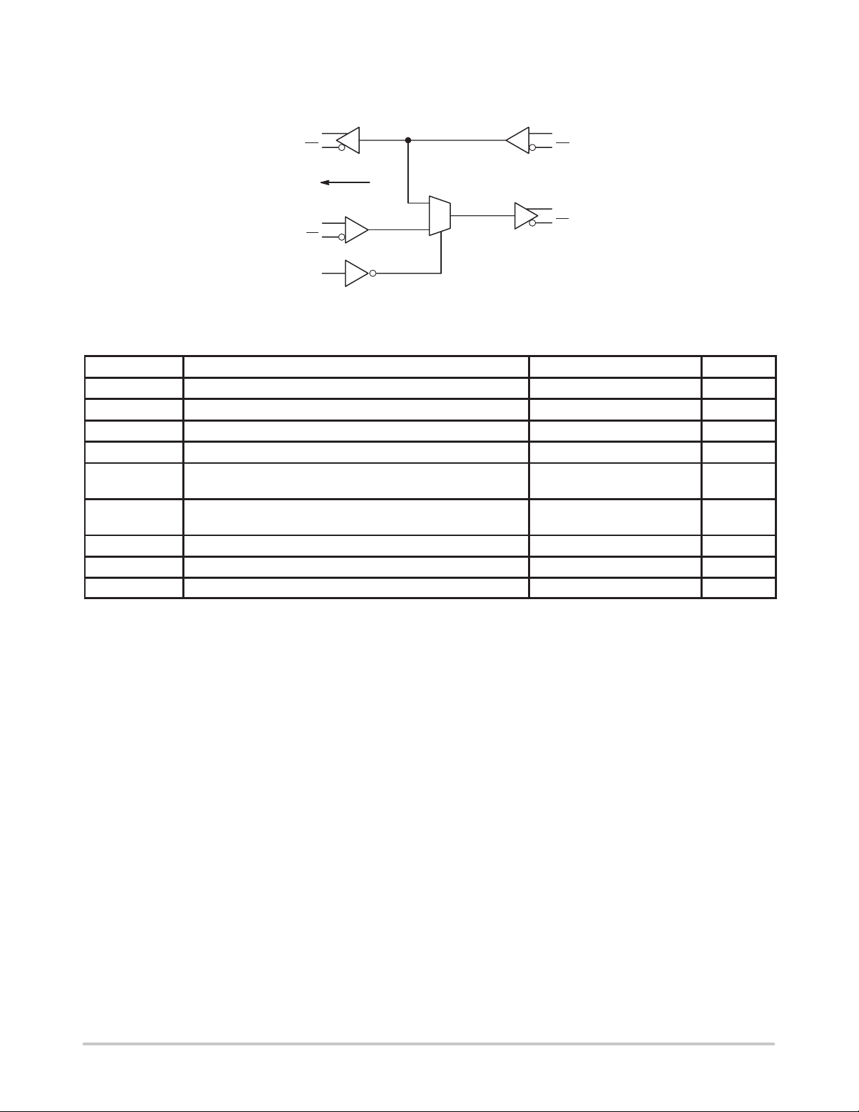
PIN DESCRIPTION
PIN
DR/DR
QR/QR ECL Buffered Differential Outputs from
DT/DT
QT/QT ECL Buffered Differential Output to
SEL
V
V
V
ECL Diff. Inputs from Receive Cable
Receive Cable
ECL Differential Input to Transmit Cable
Transmit Cable
TTL Multiplexer Control Signal
Reference Voltage Output
BB
ECL Positive Supply
CC
ECL Negative, 0 Supply
EE
A = Assembly Location
L = Wafer Lot
Y = Y ear
W = Work Week
FUNCTION
21 34567
V
DR DR
EE
Figure 1. 20-Lead TSSOP Pinout: (Top View)
This document contains information on a product under development. ON Semiconductor
reserves the right to change or discontinue this product without notice.
Semiconductor Components Industries, LLC, 1999
December, 1999 – Rev. 1
VCCV
CC
QT QT V
8
EE
SEL V
10
CC
1 Publication Order Number:
TRUTH TABLE
SEL Function
L
H
ORDERING INFORMATION
Device Package Shipping
MC10SX1 190DT TSSOP–20 75 Units/Rail
DR QT
DT QT
MC10SX1190/D
MC10SX1190
LOGIC DIAGRAM
LOCAL
RECEIVE DATA
(ECL LEVELS)
LOCAL
TRANSMIT DATA
(ECL LEVELS)
QR
QR
V
BB
DT
DT
SEL (TTL)
DR
DR
1
0
QT
QT
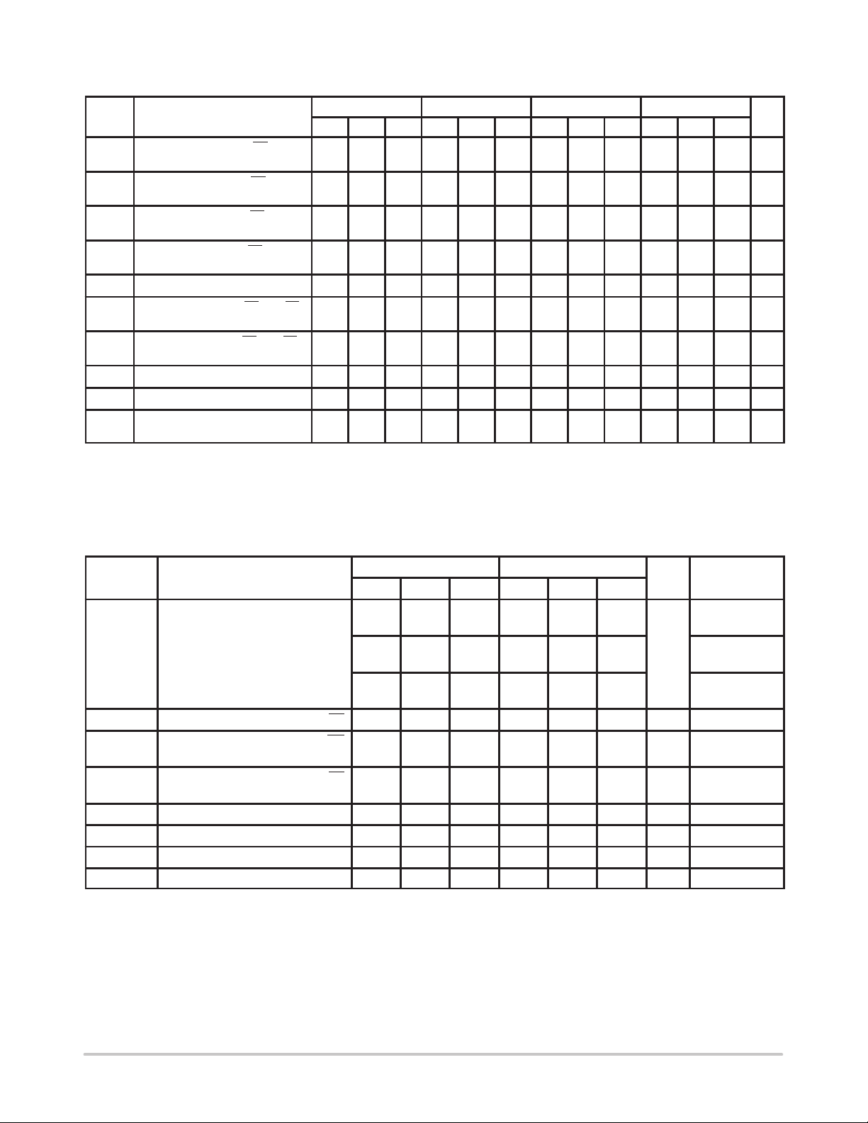
ABSOLUTE MAXIMUM RATINGS*
Symbol Parameter Value Unit
V
CC
V
EE
V
IN
V
IN
I
OUT
θJA Thermal Resistance (Junction–to–Ambient) Still Air
θJC Thermal Resistance (Junction–to–Case) 30 to 35 °C/W
T
A
T
STG
* Absolute Maximum Ratings are those values beyond which damage to the device may occur. Functional operation should be restricted to
the Recommended Operating Conditions.
Power Supply Voltage (VEE = 0V) 0 to +6.0 Vdc
Power Supply Voltage (VCC = 0V) –6.0 to 0 Vdc
Input Voltage (VEE = 0V, VIN not more positive than VCC) 0 to +6.0 Vdc
Input Voltage (VCC = 0V, VIN not more negative than VEE) –6.0 to 0 Vdc
Output Current Continuous
Surge
500 LFPM
Operating Temperature Range –40 to +85 °C
Storage Temperature Range –50 to +150 °C
FROM
INPUT CABLE
(ECL LEVELS)
TO OUTPUT
CABLE
(ENHANCED SWING)
50
100
90
60
mA
°C/W
http://onsemi.com
2
MC10SX1190
DC CHARACTERISTICS (Note 1)
-40°C 0°C 25°C 85°C
Symbol Characteristic Min Typ Max Min Typ Max Min Typ Max Min Typ Max Unit
V
V
V
V
I
CC
V
V
V
V
V
1. 10SX circuits are designed to meet the DC specifications shown in the table after thermal equilibrium has been established. The circuit is mounted in a test socket
or mounted on a printed circuit board and transverse air greater than 500lfm is maintained.
2. Values will track 1:1 with the VCC supply.
3. Outputs loaded with 50Ω to +3.0V
4. Outputs loaded with 50Ω to +2.0V
5. Outputs open circuited.
6. TTL signal threshold is 1.5V above VEE.
AC CHARACTERISTICS (Note 1 & 7)
t
PLH
t
PLH
tr,
t
f
tr,
t
f
t
skew
V
V
f
max
1. 10SX circuits are designed to meet the AC specifications shown in the table after thermal equilibrium has been established. The circuit is mounted in a test socket
or mounted on a printed circuit board and transverse air greater than 500lfm is maintained.
2. The differential propagation delay is defined as the delay from the crossing points of the differential input signals to the crossing point of the differential output
signals.
3. The single-ended propagation delay is defined as the delay from the 50% point of the input signal to the 50% point of the output signal.
4. Duty cycle skew is the difference between t
5. Minimum input swing for which AC parameters are guaranteed.
6. The CMR range is referenced to the most positive side of the differential input signal. Normal operation is obtained if the HIGH level falls within the specified range
and the peak-to-peak voltage lies between VPP
7. Data taken at V
Output Voltage High (QR,QR)
OH
OL
OH
OL
IH
IL
IH
IL
BB
VCC = 5.0V, VEE = 0V (Notes 2,3)
Output Voltage Low (QR,QR)
VCC = 5.0V, VEE = 0V (Notes 2,3)
Output Voltage High (QT,QT)
VCC = 5.0V, VEE = 0V (Notes 2,4)
Output Voltage Low (QT,QT)
VCC = 5.0V, VEE = 0V (Notes 2,4)
Quiescent Supply Current (Note 5) 55 mA
Input Voltage High (DR,DR & DT,DT)
VCC = 5.0V, VEE = 0V (Note 2)
Input Voltage Low (DR,DR & DT,DT)
VCC = 5.0V, VEE = 0V (Note 2)
Input Voltage High SEL (Note 6) 2.0 2.0 2.0 2.0 V
Input Voltage Low SEL (Note 6) 0.8 0.8 0.8 0.8 V
Output Reference Voltage
VCC = 5.0V, VEE = 0V (Note 2)
4.01 4.04 4.06 4.16 V
3.23 3.26 3.28 3.33 V
3.94 3.98 4.04 4.13 V
2.51 2.49 2.48 2.47 V
3.77 4.11 3.83 4.16 3.87 4.19 3.94 4.28 V
3.05 3.50 3.05 3.52 3.05 3.52 3.05 3.56 V
3.57 3.63 3.70 3.62 3.67 3.73 3.65 3.70 3.75 3.69 3.75 3.81 V
–40°C 0 to 85°C
Symbol Characteristic Min Typ Max Min Typ Max Unit Condition
, t
, t
Propagation Delay DR QR (Diff)
PHL
to Output (SE)
DR QT (Diff)
(SE)
DT QT (Diff)
(SE)
Propagation Delay SEL QT,QT 450 600 850 500 650 800 ps 1.5V to 50% Pt
PHL
Rise Time QR,QR
Fall Time
Rise Time QT,QT
Fall Time
240
240
425
425
425
425
118
118
230
230
ps Note 2
ps 20% to 80%
ps 20% to 80%
Note 3
80% to 20%
80% to 20%
Within Device Skew 15 15 ps Note 4
PP
CMR
Minimum Input Swing 200 200 mV Note 5
Common Mode Range 3.0 4.35 3.0 4.35 V Note 6
Maximum Operation Frequency 2.5 2.5 Gb/s
CC, nom
= 3.3V.
PLH
and t
propagation delay through a device.
PHL
and 1.0V.
Min
http://onsemi.com
3
 Loading...