

Motorola MC10SX1189D, MC10SX1189DR2 Datasheet
SEMICONDUCTOR TECHNICAL DATA
!
"
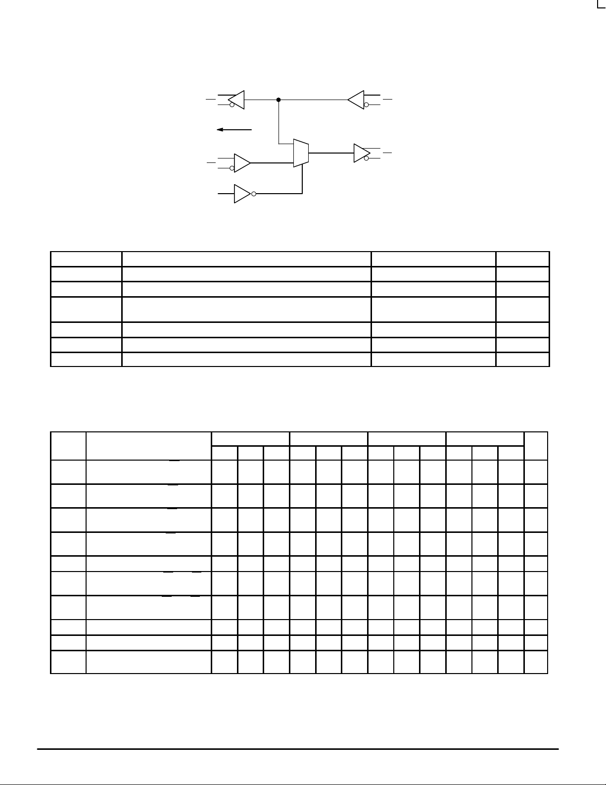
The MC10SX1189 is a differential receiver, differential transmitter
specifically designed to drive coaxial cables. It incorporates the output
cable drive capability of the MC10EL89 Coaxial Cable Driver with
additional circuitry to multiplex the output cable drive source between the
cable receiver or the local transmitter inputs. The multiplexer control
circuitry is TTL compatible for ease of operation.
• 425ps Propagation Delay
• 1.6V Output Swing on the Cable Driving Output
• Single +5V operation
• 75kΩ Internal Input Pull Down Resistors
• >1000 Volt ESD Protection
The MC10SX1189 is useful as a bypass element for Fibre
Channel-Arbitrated Loop (FC-AL) or Serial Storage Architecture (SSA)
applications, to create loop style interconnects with fault tolerant, active
switches at each device node. This device is particularly useful for back
panel applications where small size is desirable.
The EL89 style drive circuitry produces swings twice as large as a
standard PECL output. When driving a coaxial cable, proper termination
is required at both ends of the line to minimize reflections. The 1.6V
output swings allow for proper termination at both ends of the cable, while
maintaining the required swing at the receiving end of the cable. Because
of the larger output swings, the QT, QT
thevenin equivalent of 50Ω to VCC– 3.0V instead of 50Ω to VCC– 2.0V .
outputs are terminated into the
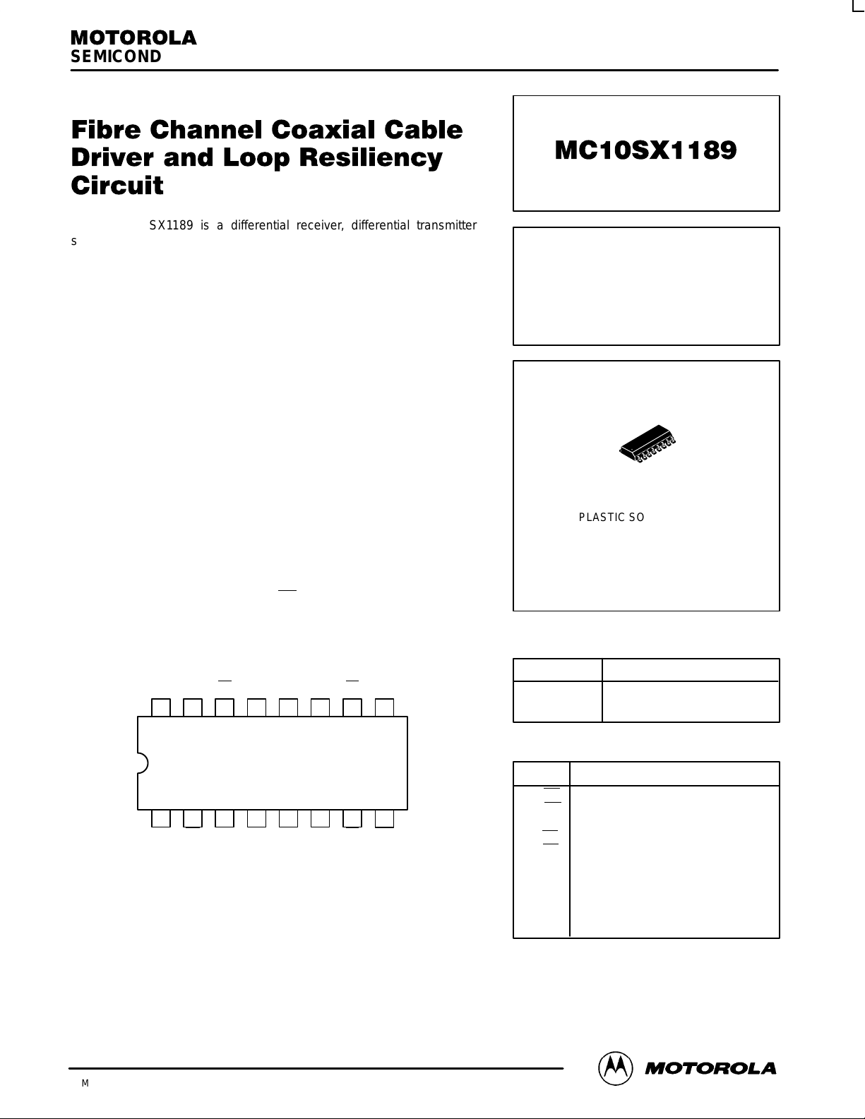
FIBRE CHANNEL COAXIAL
CABLE DRIVER AND LOOP
RESILIENCY CIRCUIT
16
1
D SUFFIX
PLASTIC SOIC PACKAGE
CASE 751B-05
DR DR
V
CC
1516 14 13 12 11 10
21 34567
QR QR
Pinout: 16-Lead SOIC (Top View)
GND VBBDT DT SEL
VCCNC VCCQT QT V
9
8
CC
TRUTH TABLE
SEL Function
L
H
PIN NAMES
Pins
DR/DR
QR/QR
DT/DT
QT/QT
SEL
V
CC
GND
V
BB
Function
Differential Input from Receive Cable
Buffered Differential Output from
Receive Cable
Differential Input to Transmit Cable
Buffered Differential Output to
Transmit Cable
Multiplexer Control Signal (TTL)
Positive Power Supply
Ground
Reference Voltage Output
DR → QT
DT → QT
3/96
Motorola, Inc. 1996
1
REV 1
MC10SX1189
LOGIC DIAGRAM
LOCAL
RECEIVE DATA
(ECL LEVELS)
LOCAL
TRANSMIT DATA
(ECL LEVELS)
V
QR
QR
BB
DT
DT
DR
DR
1
0
QT
QT
FROM
INPUT CABLE
(ECL LEVELS)
TO OUTPUT
CABLE
(ENHANCED SWING)
SEL (TTL)
ABSOLUTE MAXIMUM RATINGS*
Symbol Parameter Value Unit
V
CC
V
IN
I
OUT
T
A
T
STG
V
CC
* Absolute Maximum Ratings are those values beyond which damage to the device may occur . Functional operation should be restricted to the
Recommended Operating Conditions.
1. Parametric values specified at 4.75 to 5.25V.
Power Supply Voltage (Referenced to GND) 0 to +7.0 Vdc
Input Voltage (Referenced to GND) 0 to +6.0 Vdc
Output Current Continuous
Surge
50
100
mA
Operating Temperature Range –40 to +85 °C
Storage Temperature Range –50 to +150 °C
Operating Voltage Range
1
4.5 to 5.5 Vdc
DC CHARACTERISTICS
Symbol Characteristic Min Typ Max Min Typ Max Min Typ Max Min Typ Max Unit
V
OH
V
OL
V
OH
V
OL
I
CC
V
IH
V
IL
V
IH
V
IL
V
BB
1. 10SX circuits are designed to meet the DC specifications shown in the table after thermal equilibrium has been established. The circuit is mounted in a test socket
or mounted on a printed circuit board and transverse air greater than 500lfm is maintained.
2. Values will track 1:1 with the VCC supply.
3. Outputs loaded with 50Ω to +3.0V
4. Outputs loaded with 50Ω to +2.0V
5. Outputs open circuited.
Output Voltage High (QR,QR)
VCC = 5.0V, GND = 0V (Notes 2,3)
Output Voltage Low (QR,QR)
VCC = 5.0V, GND = 0V (Notes 2,3)
Output Voltage High (QT,QT)
VCC = 5.0V, GND = 0V (Notes 2,4)
Output Voltage Low (QT,QT)
VCC = 5.0V, GND = 0V (Notes 2,4)
Quiescent Supply Current (Note 5) 20 25 42 22 26 47 23 27 47 25 28 47 mA
Input Voltage High (DR,DR & DT,DT)
VCC = 5.0V, GND = 0V (Note 2)
Input Voltage Low (DR,DR & DT,DT)
VCC = 5.0V, GND = 0V (Note 2)
Input Voltage High SEL 2.0 2.0 2.0 2.0 V
Input Voltage Low SEL 0.8 0.8 0.8 0.8 V
Output Reference Voltage
VCC = 5.0V, GND = 0V (Note 2)
1
-40°C 0°C 25°C 85°C
3.92 4.05 4.11 3.98 4.09 4.16 4.02 4.11 4.19 4.09 4.16 4.28 V
3.05 3.23 3.35 3.05 3.24 3.37 3.05 3.24 3.37 3.05 3.25 3.41 V
3.71 3.89 4.08 3.79 3.98 4.17 3.83 4.02 4.20 3.90 4.09 4.28 V
1.94 2.22 2.50 1.83 2.12 2.41 1.80 2.10 2.39 1.77 2.06 2.35 V
3.77 4.11 3.83 4.16 3.87 4.19 3.94 4.28 V
3.05 3.50 3.05 3.52 3.05 3.52 3.05 3.56 V
3.57 3.63 3.70 3.62 3.67 3.73 3.65 3.70 3.75 3.69 3.75 3.81 V
MOTOROLA High Performance Frequency
2
Control Products — BR1334
 Loading...