

MOTOROLA MC10SX1130D, MC10SX1130DR2 Datasheet
SEMICONDUCTOR TECHNICAL DATA
Order this data sheet
by MC10SX1130/D
The MC10SX1 130 is high speed LED Driver/current switch specifically
targeted for use in FDDI PMD and ANSI X3T9.3 FibreChannel 266
Mbits/s optical transmitters. The integrated circuit contains several
unique functional blocks which makes it easily configurable for use with a
variety of high performance LED devices. The part is fabricated using
Motorola’s proven MOSAIC III advanced bipolar process. The logic is
designed so that a data HIGH input results in the modulation current
flowing through the I
• Differential Data Inputs
• 300MHz Operation
• 100mA Peak Drive Current
• Extremely Low Jitter
• Duty Cycle Distortion Compensation
• Adjustable Output Current Tracking With Temperature
• Thermally Enhanced 16-Lead SOIC Package
• 75kΩ Data Input Pulldown Resistors
• +5V or –5.2V Operation
• V
Reference Available
BB
The device incorporates open collector outputs with a capability of
driving peak currents of 100mA. Since the output current switching
circuitry simply switches current between the complementary outputs, the
dynamic switching demands on the system power supply are greatly reduced. In addition, because the design is pure bipolar, the
device current drain is insensitive to the data pattern and frequency of operation.
The LED drive current is adjustable through the selection of an external set resistor, RSET. In addition, to allow for open loop
compensation for the LED’s negative optical output power tracking over temperature, a circuit is included to provide an
adjustable positive temperature tracking coefficient to the LED drive current. This is controlled through the selection of an
external resistor, RTCO.
The MC10SX1 130 incorporates novel pulse stretching circuitry which is intended to compensate for the turn-on delay and rise
and fall time asymmetry inherent in LED devices. The stretch circuitry can be used to pre-distort the input signal pulse width to
minimize the duty cycle distortion of the transmitted optical eye pattern. The stretch circuitry supports three different selections of
pre-distortion. This choice is accomplished through a unique ‘tri-state’ input which can be left open, tied to VCC, or tied to VEE to
determine the pre-distortion amount.
The device provides a VBB output for either single-ended use or as a DC bias for AC coupling the signal into the device. The
VBB pin should only be used as a bias for the MC10SX1 130 as its current sink/source capability is limited. Whenever used, the
VBB pin should be bypassed to ground via a 0.01µF capacitor.
pin to turn on the LED.
OUT
LED DRIVER
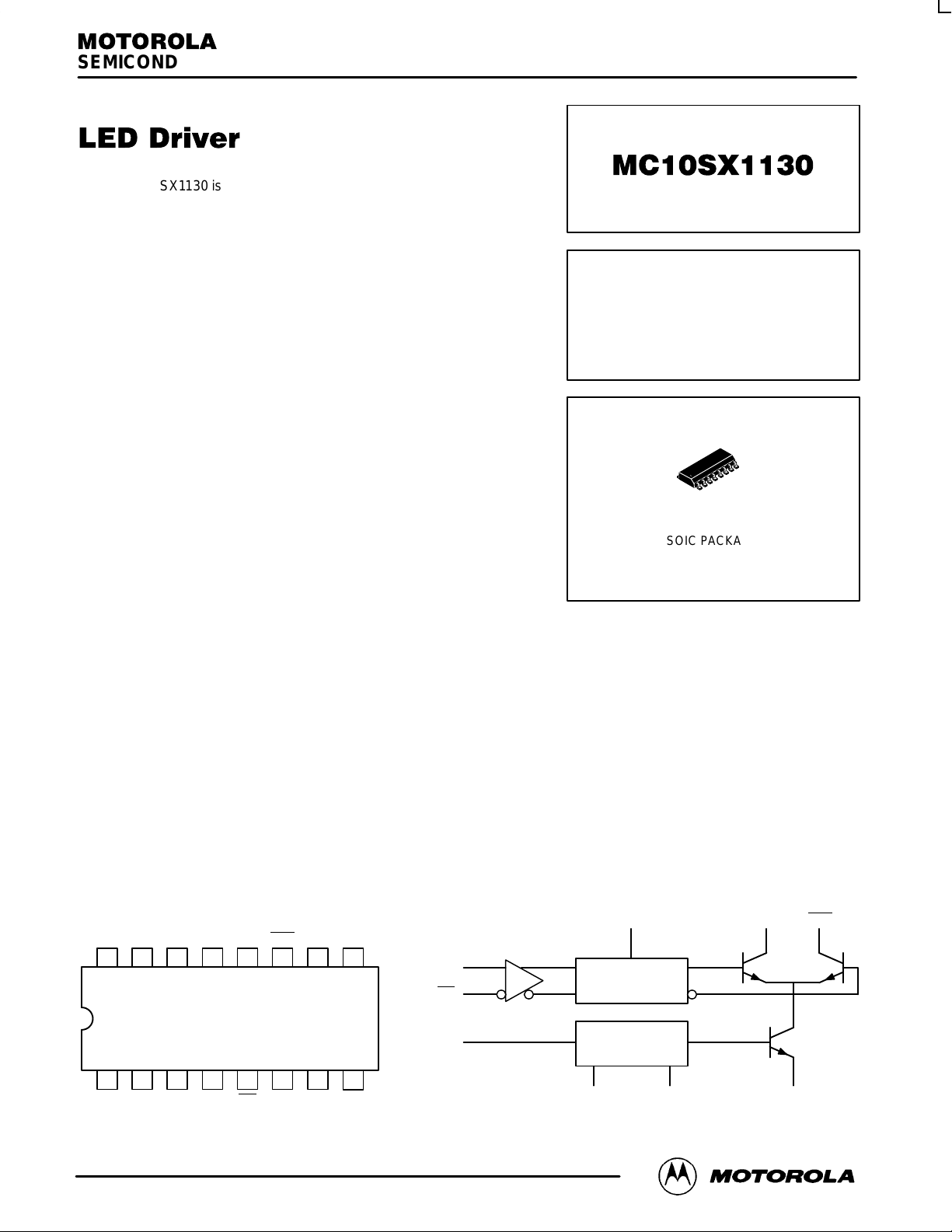
16
1
D SUFFIX
SOIC PACKAGE
CASE 751B-05
Pinout: 16-Lead Plastic Package (Top View)
Stretch VEEI
V
EE
1516 14 13 12 11 10
21 34567
VEEVCCVBBDIND
MOSAIC III is a trademark of Motorola.
3/94
OUT
RSET I
OUTVCCVEE
RTCO1RTCO2V
IN
Motorola, Inc. 1994
9
8
EE
BLOCK DIAGRAM
ECL
BUFFER
D
IN
D
IN
V
BB
Stretch
PULSE WIDTH
ADJUST CIRCUIT
BIAS
CONTROL
1
REV 1
RTCO
2
I
OUTIOUT
RSETRTCO
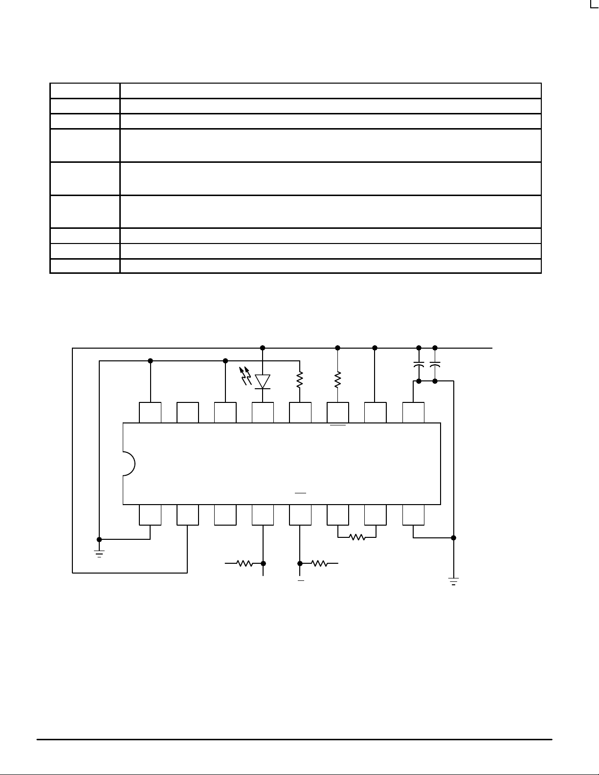
PIN FUNCTION TABLE
Pin
D
IN
I
OUT
STRETCH Control input to select the amount of duty cycle pre-distortion. When the pin is left open, no pre-distortion is introduced.
RSET Resistor to set LED drive current. This resistor sets the tail current of the output current switch and should be connected
RTCO1, RTCO
V
CC
V
EE
V
BB
Differential data inputs.
Differential open collector outputs.
If the pin is connected to VCC, the output LOW state current pulse width is increased by 155ps. When it is connected to
VEE, the current pulse width is increased by 310ps.
to the VEE plane. Since the RSET voltage compensation circuit is referenced to VEE, the RSET voltage will track 1:1 with
VEE changes, thus the voltage across the RSET resistor will remain constant.
Terminals for positive temperature tracking resistor. This resistor controls the temperature tracking rate of the voltage at
2
the RSET pin, which in turn sets the LED drive current tracking. If the two pins are shorted together, the nominal tracking
rate is 1.4mV/°C and when a 2kΩ resistor is connected across the pins, the nominal tracking rate is 4.9mV/°C.
Most positive power supply input. +5V for PECL operation or ground for standard ECL operation.
Most negative power supply input. Ground for PECL operation or –5.2V for standard ECL operation.
Reference voltage for use in single ended applications or when the input signal is AC coupled into the device.
Function
V
EE
V
EE
Stretch V
V
10
Ω
1516 14 13 12 11 10
50
I
OUT
D
IN
Ω
IN
EE
PECL
BIAS
V
BB
CC
21 34567
RSET I
D
IN
50
IN
10
Ω
OUT
RTCO1RTCO
1k
Ω
PECL
BIAS
Ω
9
V
CC
V
EE
V
2
EE
8
Figure 1. T ypical +5V Applications Circuit
SUPPLY
+5.0V
DECOUPLING
CAPACITORS
MOTOROLA High Performance Frequency
2
Control Products — BR1334
ABSOLUTE MAXIMUM RATINGS
Symbol
V
V
I
out
T
V
EE
I
A
EE
Power Supply (VCC = 0V) –7.0 to 0 VDC
Input Voltage (VCC = 0V) 0 to –6.0 VDC
Output Current Continuous
Operating Temperature Range –40 to +85 °C
Operating Range (VCC = 0) –5.5 to –4.5 VDC
*
Parameter Value Unit
Surge
* Absolute maximum rating, beyond which, device life may be impaired.
100
110
mA
DC CHARACTERISTICS1 (RTCO = 1kΩ ±5%, R
Symbol Characteristic Min Typ Max Min Typ Max Min Typ Max Min Typ Max Unit
I
IH
I
IL
I
CC
V
IH
V
IL
V
BB
V
SET
IO
IO
V
TR
1. 10SX circuits are designed to meet the DC specifications shown in the table after thermal equilibrium has been established. The circuit is mounted in a test socket
or mounted on a printed circuit board and transverse air greater than 500lfm is maintained.
2. Note that in PECL applications, VIH, VIL, VBB will vary 1:1 with the VCC supply.
3. V
4. VTR tracking measures the rate of change of the V
Input HIGH Current
(DIN, DIN
Input LOW Current
(DIN, DIN
Quiescent Supply Current
(No Load on RSET Pin)
Input HIGH Voltage
Input LOW Voltage
Output Reference Voltage
Output Voltage at RSET Pin
VCC = 5.0V, RTCO = Short
VEE = GND RTCO = 1kΩ
VCC = GND
VEE = –5.2V RTCO = 1kΩ
Output ‘ON’ Current
on
(IOUT, IOUT
Output ‘OFF’ Current
off
(IOUT, IOUT
VSET Tracking
tracks 1:1 with the VEE supply to maintain the same voltage across the RSET resistor.
SET
Pins)
Pins)
2
VCC = 5.0V, VEE = GND
VCC = GND, VEE = -4.5 to -5.5V
2
VCC = 5.0V, VEE = GND
VCC = GND, VEE = -4.5 to -5.5V
2
VCC = 5.0V, VEE = GND
VCC = GND, VEE = -4.5 to -5.5V
RTCO = 2kΩ
3
Pins)
Pins)
Short Between RTCO1 and RTCO2
1kΩ Between RTCO1 and RTCO2
2kΩ Between RTCO1 and RTCO2
RTCO = Short
RTCO = 2kΩ
4
0.5 0.5 0.5 0.5
12 17 24 12 17 24 12 18 24 12 19 24
3770
-1230
3050
-1950
3570
-1430
30 75 30 75 30 75 30 100
voltage over temperature.
SET
= R at I
SET
-40°C 0°C 25°C 85°C
200 200 200 200
4110
-890
3500
-1500
3700
-1300
600
430
230
-4400
-4570
-4770
50 50 50 50
1.4
3.4
4.9
OUT
3830
-1170
3050
-1950
3620
-1380
= R at I
635
515
355
-4365
-4485
-4645
1.4
3.4
4.9
= 10Ω ±1%, Unless Otherwise Noted)
OUT
4160
-840
3520
-1480
3730
-1270
3870
-1130
3050
-1950
3650
-1350
610
570
470
-4390
-4430
-4530
690
650
550
-4310
-4350
-4450
1.4
3.4
4.9
4190
-810
3520
-1480
3750
-1250
770
730
630
-4230
-4270
-4370
3940
-1060
3050
-1950
3690
-1310
775
855
845
-4225
-4145
-4155
1.4
3.4
4.9
µA
µA
mA
mV
4280
-720
mV
3555
-1445
mV
3810
-1190
mV
mA
µA
mV/
°C
Control Products — BR1334
MOTOROLAHigh Performance Frequency
3
 Loading...