

MOTOROLA MC10SX1125D, MC10SX1125DR2 Datasheet
SEMICONDUCTOR TECHNICAL DATA
1
REV 1
Motorola, Inc. 1996
5/96
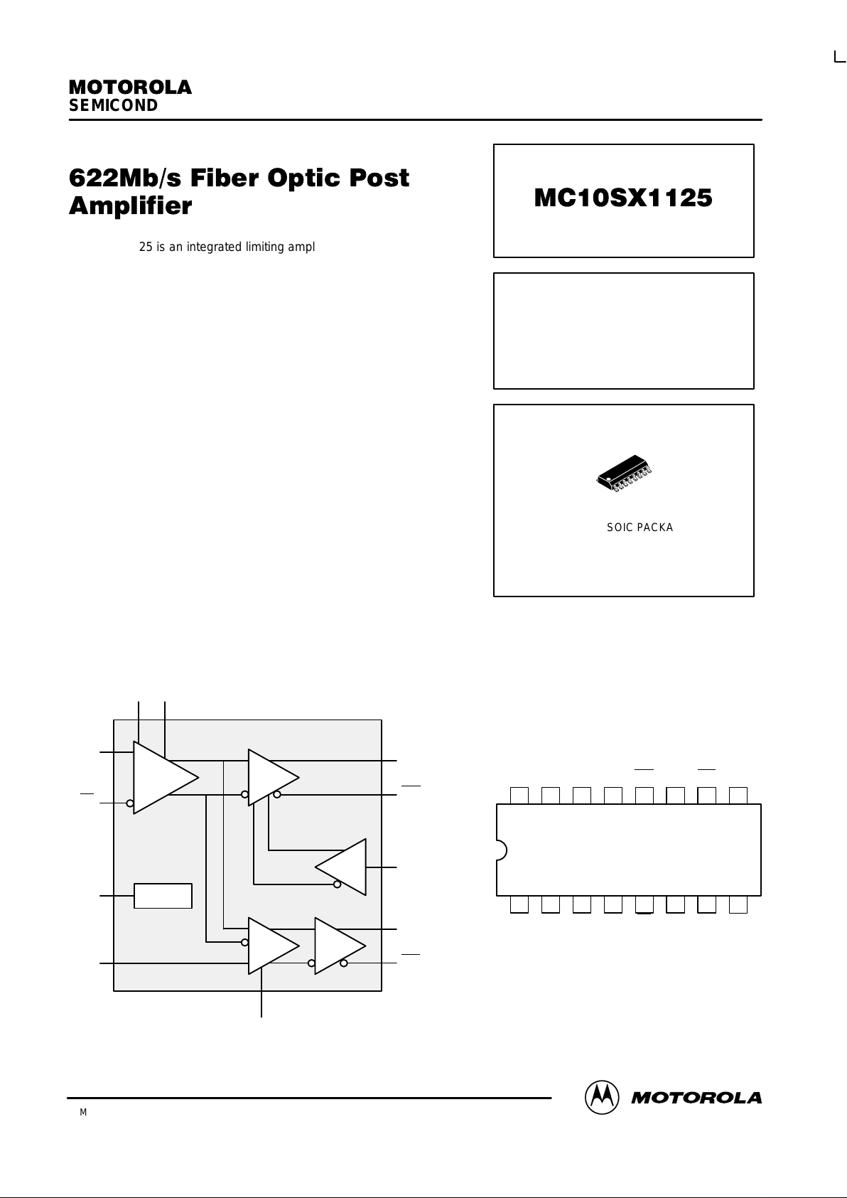
The SX1125 is an integrated limiting amplifier for high frequency fiber
optic applications. The device interfaces directly to the trans–impedance
amplifier of a typical optical to electrical conversion portion of a fiber optic
link. With data rate capabilities in the 622Mb/s range, the high gain
limiting amplification of the SX1125 is ideal for high speed fiber optic
applications like SONET/SDM, A TM, FDDI, Fibre Channel or Serial Hippi.
The device is functionally and pin compatible to the Signetics SA5225
with a significantly higher bandwidth. The C
AZP
and C
AZN
inputs to the
limiting amplifier provide an auto-zero function to effectively cancel any
input offset voltage present in the amplifier.
The SX1125 incorporates a programmable level detect function to
identify when the input signal has been lost. This information can be fed
back to the Disable input of the device to maintain stability under loss of
signal conditions. Using the V
set
pin the sensitivity of the level detect can
be adjusted. The CLD input is used to filter the level detect input so that
random noise spikes are filtered out.
The MC10SX1125 is compatible with MECL10H logic levels.
• Wideband Operation: 20kHz to 550MHz
• Programmable Input Signal Level Detection
• Operation with single +5V or standard ECL supply
• Standard 16-lead SOIC Package
• Fully Differential Design to Minimize Noise Affects
• 10KH Compatible
BLOCK DIAGRAM
LOS
LOS
D
out
D
out
Reference
ECL
Buffer
Level
Detect
Limiting
Amplifier
ECL
Buffer
Disable
Disable
C
LD
D
in
D
in
V
ref
V
set
C
AZPCAZN
1516 14 13 12 11 10
21 34567
V
set
9
8
V
refVCCEDout
D
out
GNDELOS LOS
C
AZNCAZP
GNDADinD
in
V
CCACLD
Disable
Pinout: 16-Lead Plastic Package
(Top View)
FIBER OPTIC
POST AMPLIFIER
D SUFFIX
PLASTIC SOIC PACKAGE
CASE 751B-05
MC10SX1125
MOTOROLA ECLinPS and ECLinPS Lite
DL140 — Rev 3
2
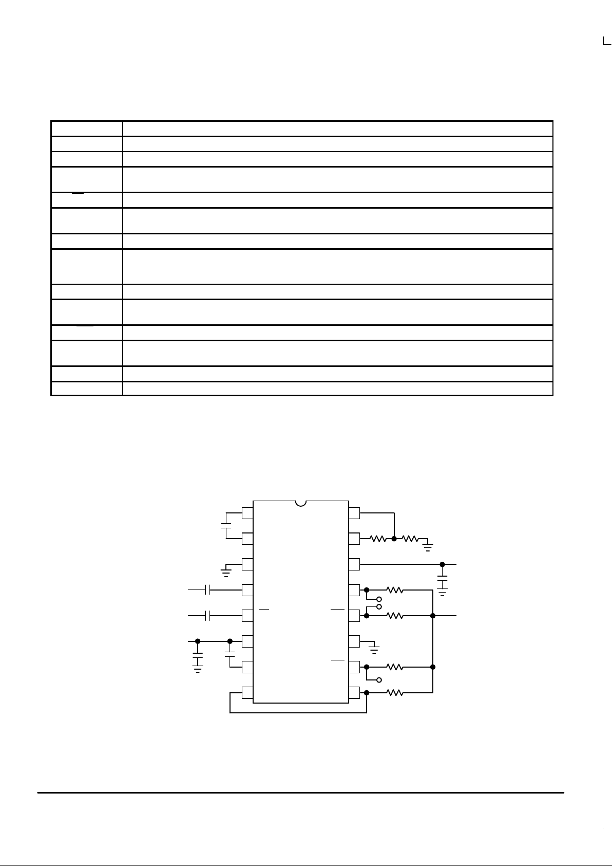
FUNCTION TABLE
Pin Function
C
AZN
Auto-zero capacitor pin. A capacitor between this pin and C
AZP
cancels any offset inherent to the limiting amplifier.
C
AZP
Auto-zero capacitor pin. A capacitor between this pin and C
AZN
cancels any offset inherent to the limiting amplifier.
GND
A
Analog ground pin. Ground for PECL operation or –5.2V for standard ECL operation. GNDA and GNDE must be at the same
potential.
Din, D
in
Differential data input.
V
CCA
Analog power supply pin. +5V for PECL operation or ground for standard ECL operation. V
CCA
and V
CCE
must be at the
same potential.
C
LD
Filter capacitor for the level detect comparator. Capacitor should be connected to V
CCA
.
Disable When asserted LOW, or left open and pulled LOW via the input pulldown resistor , the output buffer will be enabled and will
respond to the input stimulus on the Din input. Forcing Disable HIGH will force the D
out
output LOW and its complimentary
output HIGH.
LOS Loss of signal. This output will go HIGH when the input signal falls below (V
set
/100) mV
P-P
.
GND
E
Digital ground pin. Ground for PECL operation or –5.2V for standard ECL operation. GNDA and GNDE must be at the same
potential.
D
out
, D
out
Differential data outputs.
V
CCE
Digital power supply pin. +5V for PECL operation or ground for standard ECL operation. V
CCA
and V
CCE
must be at the
same potential.
V
ref
Reference voltage for threshold level set voltage division network (2.64V).
V
set
Input threshold level detect setting input. Input generated from voltage divider between V
ref
and GNDA.
Figure 1. Typical Operating Circuit
161
C
AZN
V
set
152
C
AZP
V
ref
143
GND
A
V
CCE
134
D
in
D
out
125
D
in
D
out
116
V
CCA
GND
E
107
C
LD
LOS
98
Disable LOS
R1 R2
50
DATA OUT
50
5V
3V
50
LEVEL
DETECT OUT
50
C
bypass
C
AZ
C
in
C
in
DATA IN
5V
C
AZ
C
bypass
 Loading...