

Motorola MC10H681FN, MC100H681FN Datasheet
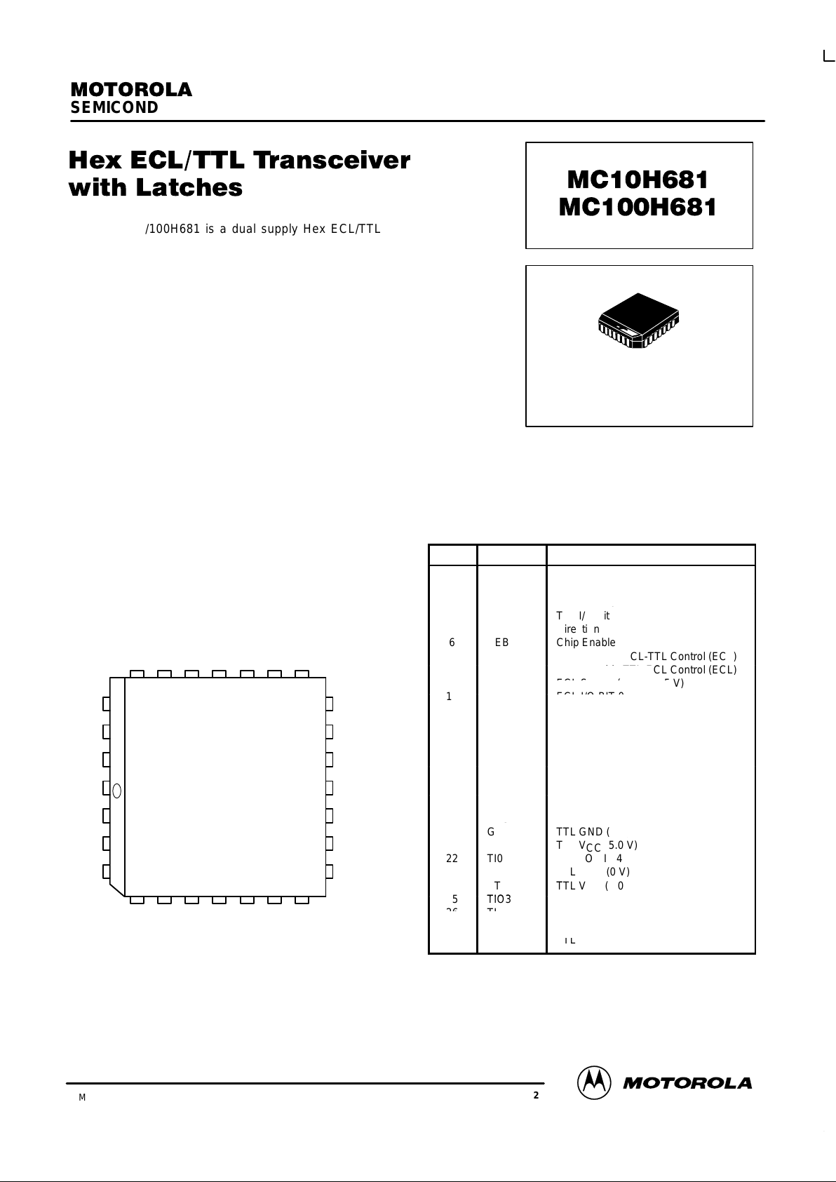
SEMICONDUCTOR TECHNICAL DATA
2–316
REV 2
Motorola, Inc. 1996
9/96
The MC10/100H681 is a dual supply Hex ECL/TTL transceiver with
latches in both directions. ECL controlled Direction and Chip Enable Bar
pins. There are two Latch Enable pins, one for each direction.
The ECL outputs are single ended and drive 50 Ω. The TTL outputs are
specified to source 15 mA and sink 48 mA, allowing the ability to drive highly
capacitive loads. The high driving ability of the TTL outputs make the device
ideal for bussing applications.
The ECL output levels are standard VOH and VOL cutoff equal to –2.0 V
(VTT). When the ECL ports are disabled the outputs go to the VOL cutoff
level. Multiple ECL V
CCO
pins are utilized to minimize switching noise.
The TTL ports have standard levels. The TTL input receivers have PNP
input devices to significantly reduce loading. Multiple TTL power and ground
pins are utilized to minimize switching noise.
The 10H version is compatible with MECL 10H ECL logic levels. The
100H version is compatible with 100K levels.
• Separate Latch Enable Controls for each Direction
• ECL Single Ended 50 Ω I/O Port
• High Drive TTL I/O Ports
• Extra TTL and ECL Power/Ground Pins to Minimize
Switching Noise
• Dual Supply
• Direction and Chip Enable Control Pins
Pinout: 28–Lead PLCC (Top View)
1
567891011
25 24 23 22 21 20 19
26
27
28
2
3
4
12
13
14
15
16
17
18
TIO2
VT
GT
TIO1
VT
GT
TIO0
EIO5
V
CCO
EIO4
V
CCE
EIO3
V
CCO
EIO2
TIO3
VT
GT
TIO4
VT
GT
TIO5
DIR
LEET
EIO1
CEB
LETE
EIO0
V
EE
Pin Symbol Description
1 TI01 TTL I/O BIT 1
12TI01VTTTL I/O BIT 1
TTL V
(5.0 V
)
23VTGTTTL V
CC
(5.0
V)
TTL GND (0 V)
34GT
TI00
TTL GND (0 V)
TTL I/O Bit 0
45TI00
DIR
TTL I/O Bit 0
Direction Control (ECL)
6 CEB
()
Chip Enable Bar Control (ECL)
7
LEET
p()
Latch Enable ECL-TTL Control (ECL)
8
LETE
Latch Enable TTL-ECL Control (ECL)
9
V
EE
ECL Supply (–5.2/–4.5 V)
10
EI00
ECL I/O BIT 0
11
EI01
ECL I/O BIT 1
12
EI02
ECL I/O BIT 2
—
13
V
CCO
ECL V
CC
(0 V)
— Outputs
14
EIO3
TTL I/O BIT 3
1516V
CCE
EIO4
ECL V
CC
(0
V)
ECL I/O BIT 4
1617EIO4VECL I/O BIT 4
ECL V
(0 V) — Outputs
1718V
CCO
EIO5
ECL V
CC
(0 V) —
Outputs
ECL I/O BIT 5
1819EIO5
TI05
ECL I/O BIT 5
TTL I/O BIT 5
1920TI05GTTTL I/O BIT 5
TTL GND (0 V)
021GVTG(0)
TTL VCC (5.0 V)
22
TI04
CC
()
TTL I/O BIT 4
23
GT
TTL GND (0 V)
24
VT
TTL VCC (5.0 V)
25
TIO3
TTL I/O BIT 3
26
TIO2
TTL I/O BIT 2
27
VT
TTL VCC (5.0 V
)
28GTTTL V
CC
(0
V)
FN SUFFIX
PLASTIC PACKAGE
CASE 776–02
MC10H681 MC100H681
2–317 MOTOROLAMECL Data
DL122 — Rev 6
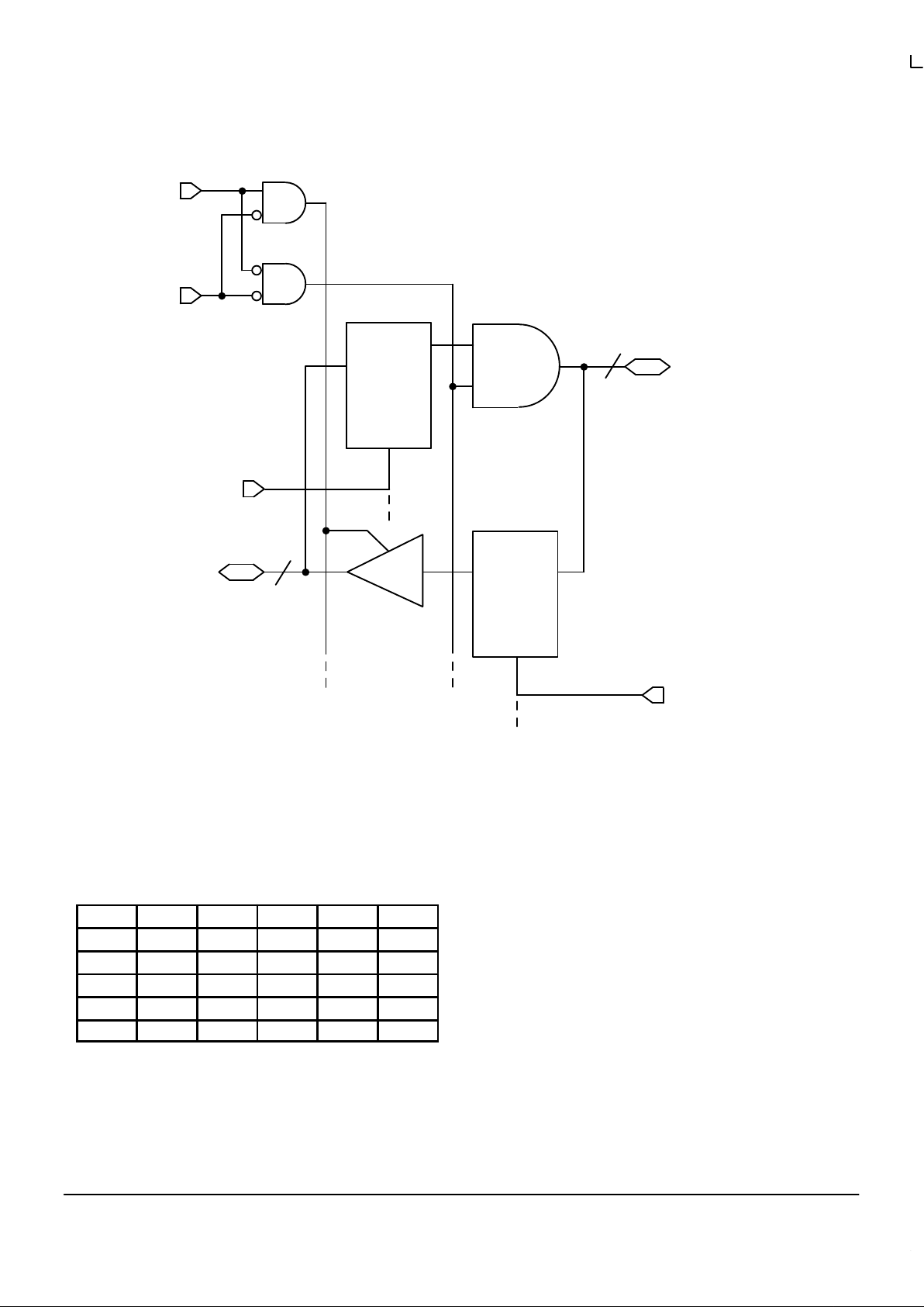
DIR
CE
LE-TE
TIO
D
Q
6
EIO
LE-ET
6
TOE
EOE
QD
LE
TRUTH TABLE
CEB DIR LEET LETE EOUT TOUT
H X X X Z Z
L H L L Z EIN
L H H L Z Qo
L L L L TIN Z
L L L H Qo Z
• Hex
• Bi-Directional
• ECL/TTL Translation
• Dual Supply
• ECL Outputs, 50 Ohm S.E., VOH/Cutoff
• TTL Outputs, 48 mA Sink, 15 mA Source
• Multi Power and Ground Pins
• Separate LE Controls
MC10H681 MC100H681
MOTOROLA MECL Data
DL122 — Rev 6
2–318
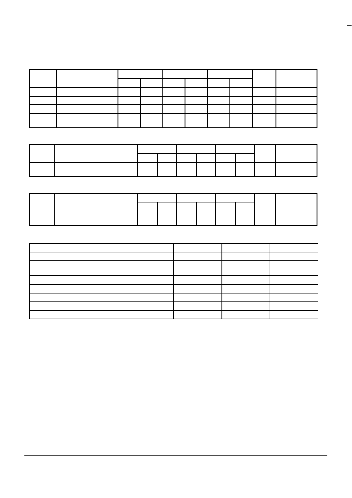
ECL DC CHARACTERISTICS: V
CCT
= +5.0 V ±10%, VEE = –5.2 ±5% (10H Version); VEE = –4.2 V to –5.5 V (100H Version)
Test
TA = 0°C TA = 25°C TA = 75°C
Test
Symbol
Parameter Min Max Min Max Min Max Unit Condition
I
EE
Supply Current/ECL — –113 — –113 — –113 mA
I
INH
Input HIGH Current — 225 — 145 — 145 µA
I
INL
Input LOW Current 0.5 — 0.5 — 0.3 — µA
V
OH
V
OL
Output HIGH Voltage
Output LOW Voltage
–1020
–2.1
–840
–2.03
–980
–2.1
–810
–2.03
–920
–2.1
–735
–2.03
mV
V
50 Ω to –2.1 V
10H ECL DC CHARACTERISTICS: V
CCT
= +5.0 ±10%, VEE = –5.2 ±5%
Test
TA = 0°C TA = 25°C TA = 75°C
Test
Symbol
Parameter Min Max Min Max Min Max Unit Condition
V
IH
V
IL
Input HIGH Voltage
Input LOW Voltage
–1170
–1950
–840
–1480
–1130
–1950
–810
–1480
–1070
–1950
–735
–1450
mV
100H ECL DC CHARACTERISTICS: V
CCT
= +5.0 ±10%, VEE = –4.2 V to –5.5 V
Test
TA = 0°C TA = 25°C TA = 75°C
Test
Symbol
Parameter Min Max Min Max Min Max Unit Condition
V
IH
V
IL
Input HIGH Voltage
Input LOW Voltage
–1165
–1810
–880
–1475
–1165
–1810
–880
–1475
–1165
–1810
–880
–1475
mV
ABSOLUTE RATINGS (Do not exceed):
Power Supply Voltage VEE (ECL) –8.0 to 0 Vdc
Power Supply Voltage V
CCT
(TTL) –0.5 to +7.0 Vdc
Input Voltage VI (ECL)
VI (TTL)
0.0 to V
EE
–0.5 to +7.0
Vdc
Disabled 3-State Output V
out
(TTL) 0.0 to V
CCT
Vdc
Output Source Current Continuous I
out
(ECL) 100 mAdc
Output Source Current Surge I
out
(ECL) 200 mAdc
Storage Temperature T
stg
–65 to 150 °C
Operating Temperature T
amb
0.0 to +75 °C
 Loading...