

Motorola MC10H680FNR2, MC10H680FN, MC100H680FN Datasheet
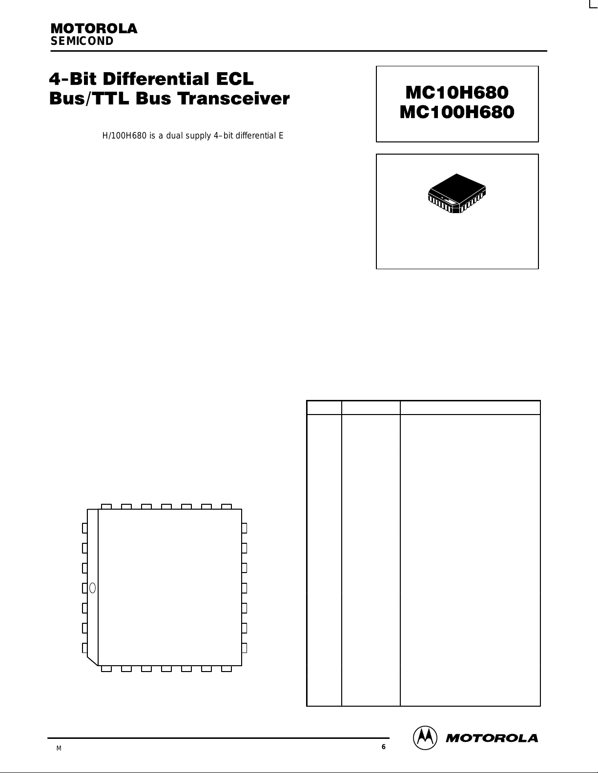
SEMICONDUCTOR TECHNICAL DATA
The MC10H/100H680 is a dual supply 4–bit differential ECL bus to TTL
bus transceiver. It is designed to allow the system designer to no longer be
limited in bus speed associated with standard TTL busses. Using a
differential ECL Bus will increase the frequency of operation and increase
noise immunity .
Both the TTL and the ECL ports are capable of driving a bus. The ECL
outputs have the ability to drive 25 Ω, allowing both ends of the bus line to be
terminated in the characteristic impedance of 50 Ω. The TTL outputs are
specified to source 15 mA and sink 48 mA, allowing the ability to drive highly
capacitive loads.
The ECL output levels are VOH approximately equal to –1.0 V and V
cutoff equal to –2.0 V (VTT). When the ECL ports are disabled both EIOx and
EIOxB go to the VOL cutoff level. The ECL input receivers have special
circuitry which detects this disabled condition, prevents oscillation, and
forces the TTL output to the low state. The noise margin in this disabled state
is greater than 600 mV. Multiple ECL V
pins are utilized to minimize
CCO
switching noise.
The TTL ports have standard levels. The TTL input receivers have PNP
input devices to significantly reduce loading. Multiple TTL power and ground
pins are utilized to minimize switching noise.
The control pins (EDIR and ECEB) of the 10H version is compatible with
MECL 10H ECL logic levels. The control pins of the 100H version are
compatible with 100K levels.
OL
FN SUFFIX
PLASTIC PACKAGE
CASE 776–02
• Differential ECL Bus (25 Ω) I/O Ports
• High Drive TTL Bus I/O Ports
• Extra TTL and ECL Power/Ground Pins to Minimize
Switching Noise
• Dual Supply
• Direction and Chip Enable Control Pins
Pinout: 28–Lead PLCC (Top View)
TIO2
GT3
VT2
25 24 23 22 21 20 19
T101
26
27
GT2
28
VT1
1
GT1
2
TIO0
3
TDIR
412
EDIR
567891011
EIO0
CCO1
EIO0B
V
GT4
EE
V
TIO3
EI01
TCEB
CCO2
V
ECEB
18
17
16
15
14
13
EIO1B
EIO3B
V
EIO3
V
EIO2B
V
EIO2
CCO4
CCE
CCO3
PIN DESCRIPTIONS
Pin Symbol Function
1 GT1 TTL Ground 1
2 TIO0 TTL I/O Bit 0
3 TDIR TTL Direction Control
4 EDIR ECL Direction Control
5 EIO0 ECL I/O Bit 0
6 VCCO1 ECL VCC 1 (0V) – Outputs
7 EIO0B ECL I/O Bit 0 Bar
8 VEE ECL Supply (–5.2/–4.5V)
9 EIO1 ECL I/O Bit 1
10 VCCO2 ECL VCC 2 (0V) – Outputs
11 EIO1B ECL I/O Bit 1 Bar
12 EIO2 ECL I/O Bit 2
13 VCCO3 ECL VCC 3 (0V) – Outputs
14 EIO2B ECL I/O Bit 2 Bar
15 VCCE ECL VCC (0V)
16 EIO3 ECL I/O Bit 3
17 VCCO4 ECL VCC 4 (0V) – Outputs
18 EIO3B ECL I/O Bit 3 Bar
19 ECEB ECL Chip Enable Bar Control
20 TCEB TTL Chip Enable Bar Control
21 TIO3 TTL I/O Bit 3
22 GT4 TTL Ground 4
23 VT2 TTL Supply 2 (5V)
24 GT3 TTL Ground 3
25 TIO2 TTL I/O Bit 2
26 TIO1 TTL I/O Bit 1
27 GT2 TTL Ground 2
28 VT1 TTL Supply 1 (5V)
9/96
Motorola, Inc. 1996
2–144
REV 6
TRUTH TABLE
MC10H680 MC100H680
TDIR — Direction Control TTL Levels
EDIR — Direction Control ECL Levels
TCEB — Chip Enable Bar Control TTL Levels
ECEB — Chip Enable Bar Control ECL Levels
TIN — TTL Input
TOUT — TTL Output
EIN — ECL Input
EINB — ECL Input Bar
EOUT — ECL Output
EOUTB — ECL Output Bar
ECEB
TCEB EDIR TDIR EIN EINB EOUT EOUTB TIN TOUT COMMENTS
H X X X X X LC LC X Z ECL and TTL Outputs Disabled
X H X X X X LC LC X Z ECL and TTL Outputs Disabled
L L H X H LC NA H ECL to TTL Direction
L L H X LC H NA L ECL to TTL Direction
L L H X LC LC NA L ECL to TTL Direction (L–L Cond.)
L L X H H LC NA H ECL to TTL Direction
L L X H LC H NA L ECL to TTL Direction
L L X H LC LC NA L ECL to TTL Direction (L–L Cond.)
L L L L NA NA H LC H TTL to ECL Direction
L L L L NA NA LC H L TTL to ECL Direction
H — HIGH
L — LOW
LC — ECL Low Cutoff (VTT = –2.0 V)
X — Don’t Care
Z — High Impedance
ABSOLUTE RATINGS (Do not exceed):
Power Supply Voltage VEE (ECL) –8.0 to 0 Vdc
Power Supply Voltage V
Input Voltage VI (ECL)
Disabled 3–State Output V
Output Source Current Continuous I
Output Source Current Surge I
Storage Temperature T
Operating Temperature T
(TTL) –0.5 to +7.0 Vdc
CCT
0.0 to V
VI (TTL)
(TTL) 0.0 to V
out
(ECL) 100 mAdc
out
(ECL) 200 mAdc
out
stg
amb
EE
–0.5 to +7.0
CCT
–65 to 150 °C
0.0 to +75 °C
Vdc
Vdc
DL122 — Rev 6
2–145 MOTOROLAMECL Data
MC10H680 MC100H680
Test
Test
Test
Test
Test
ECL DC CHARACTERISTICS: V
Test
Symbol
I
EE
I
INH
I
INL
V
OH
V
OL
Supply Current/ECL –110 –110 –110 mA
Input HIGH Current 225 145 145 µA
Input LOW Current 0.5 0.5 0.3 µA
Output HIGH Voltage
Output LOW Voltage
Parameter Min Max Min Max Min Max Unit Condition
CCT
CONTROL INPUTS ONLY
10H ECL DC CHARACTERISTICS:
Test
Symbol
V
IH
V
IL
Input HIGH Voltage
Input LOW Voltage
Parameter Min Max Min Max Min Max Unit Condition
CONTROL INPUTS ONLY
100H ECL DC CHARACTERISTICS:
Test
Symbol
V
IH
V
IL
Input HIGH Voltage
Input LOW Voltage
Parameter Min Max Min Max Min Max Unit Condition
= +5.0 V ±10%, VEE = –5.2 ±5% (10H Version); VEE = –4.2 V to –5.5 V (100H Version)
TA = 0°C TA = 25°C TA = 75°C
–1100
–2.1
V
= +5.0 ±10%, VEE = –5.2 ±5%
CCT
–1170
–1950
V
= +5.0 ±10%, VEE = –4.2 V to –5.5 V
CCT
–1165
–1810
–840
–2.03
TA = 0°C TA = 25°C TA = 75°C
–840
–1480
TA = 0°C TA = 25°C TA = 75°C
–880
–1475
–1100
–2.1
–1130
–1950
–1165
–1810
–810
–2.03
–810
–1480
–880
–1475
–1100
–2.1
–1070
–1950
–1165
–1810
–735
–1450
–880
–1475
–735
–2.03
mVV25 Ω to –2.1 V
mV
mV
TTL DC CHARACTERISTICS: V
Test
Symbol
V
IH
V
IL
V
IK
V
OH
V
OL
IIH* TTL (Input HIGH)
IIL* TTL (Input LOW) –0.6 –0.6 –0.6 mA Vin = 0.5 V
I
CCL
I
CCH
I
CCZ
I
OS
* NOTE: TTL Control Inputs only
Standard Input
Standard Input
Input Clamp –1.2 –1.2 –1.2 Vdc IIN = –18 mA
Output HIGH Voltage
Output HIGH Voltage
Output LOW Voltage 0.55 0.55 0.55 V IOL = 48 mA
TTL (Input HIGH)
Supply Current 75 75 75 mA
Supply Current 70 70 70 mA
Supply Current 70 70 70 mA
Output Short Circuit Current –100 –225 –100 –225 –100 –225 mA V
Parameter Min Max Min Max Min Max Unit Condition
= +5.0 V ±10%, VEE = –5.2 ±5% (10H Version); VEE = –4.2 V to –5.5 V (100H Version)
CCT
TA = 0°C TA = 25°C TA = 75°C
2.0
0.8
2.5
2.0
20
100
2.0
2.5
2.0
0.8
20
100
2.0
2.5
2.0
0.8
20
100
Vdc
V IOH = –3.0 mA
µA Vin = 2.7 V
IOH = –15 mA
Vin = 7.0 V
OUT
TTL I/O DC CHARACTERISTICS ONLY
Test
Symbol
I
IH/IOZH
I
IL/IOZL
Parameter Min Max Min Max Min Max Unit Condition
Output Disable
Current
TA = 0°C TA = 25°C TA = 75°C
70
200
70
200
70
200
µA V
V
OUT
OUT
= 0 V
= 2.7 V
= 0.5 V
MOTOROLA MECL Data
2–146
DL122 — Rev 6
 Loading...