

Motorola MC10H660FN, MC100H660FN Datasheet
SEMICONDUCTOR TECHNICAL DATA
2–121
REV 5
Motorola, Inc. 1996
3/93
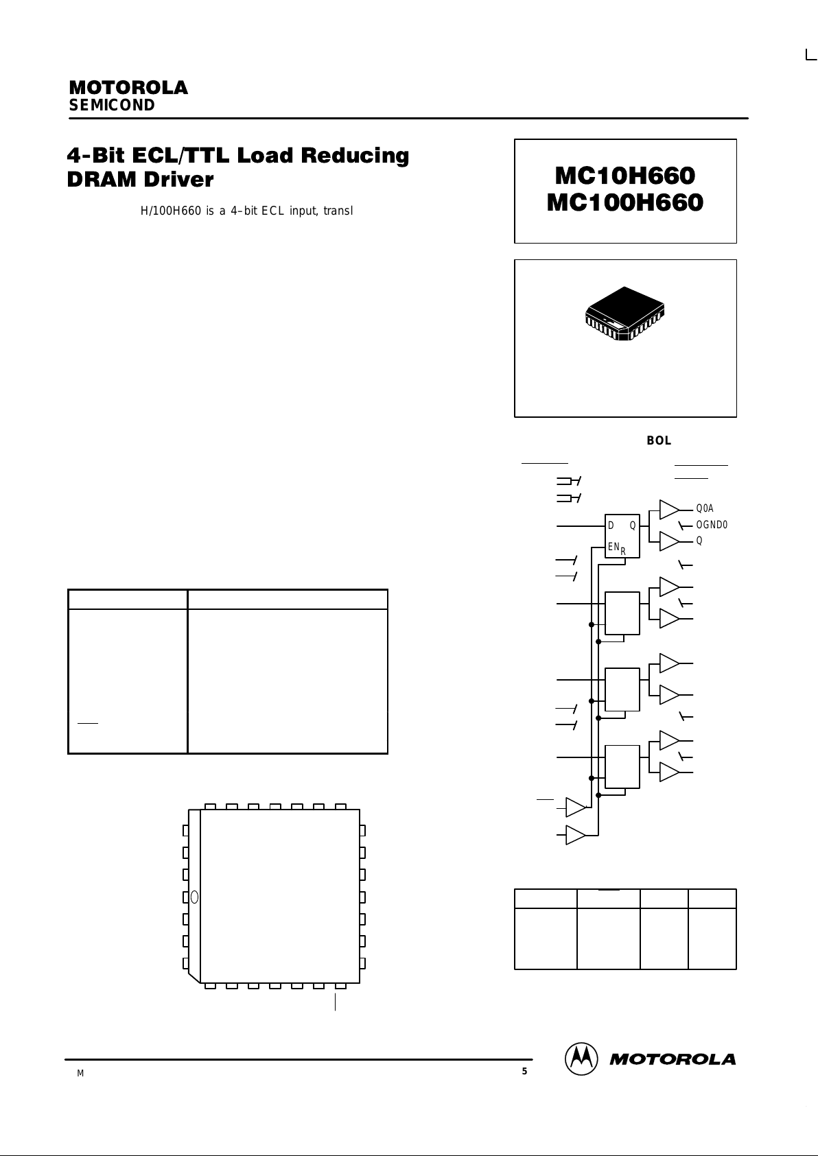
The MC10H/100H660 is a 4–bit ECL input, translating DRAM address
driver, ideally suited for driving TTL compatible DRAM inputs from an ECL
system. It is designed for use in high capacity, highly interleaved DRAM
memory boards, that directly interface to a high speed, pipelined ECL bus
interface, where new operations may be initiated to the board at up to a 50
MHz rate.
The latch provides the capability for the memory controller to propagate
new addresses to different banks without having to wait for the address timing
constraints to be satisfied from a previous memory operation. The dual output
fanout reduces input loading from the controller by a factor of two, thus
significantly improving board etch propagation delays from the controller,
without the need for additional ECL buffering.
The H660 features special TTL outputs which do not have an IOS limiting
resistor, therefore allowing rapid charging of the load capacitance. Output
voltage levels are designed specifically for driving DRAM inputs. The output
stages feature separate power and ground pins to isolate output switching
noise from internal circuitry, and also to improve simultaneous switching
performance.
The 10H version is compatible with MECL 10H ECL logic levels. The
100H version is compatible with 100K levels.
• High Capacitive Drive Outputs to Drive DRAM Address Inputs
• Extra TTL and ECL Power/Ground Pins to Minimize Switching Noise
• Dual Supply
• 10.7 ns Max. D to Q into 300 pF
PIN NAMES
PIN FUNCTION
OGND[0:3] Output Ground (0V)
OVT01, OVT23 Output VCCT (+5.0 V)
IGND01, IGND23 Internal TTL Ground (OV)
IVT01, IVT23 Internal TTL VCCT (+5.0 V)
VEE ECL Neg. Supply (–5.2/ –4.5 V)
VCCE ECL Ground (0V)
D[0:3] Data Inputs (ECL)
Q[0:3]A, Q[0:3]B Data Outputs (TTL levels)
LEN Latch Enable (ECL)
R Reset (ECL)
Q2A
OGND2
Q2B
OVT23
Q3A
OGND3
Q3B
IVT01
IGND01
VEE
VEE
D0
LEN
D1
1
567891011
25 24 23 22 21 20 19
Pinout: 28–Lead PLCC
(Top View)
26
27
28
2
3
412
13
14
15
16
17
18Q1B
OGND1
Q1A
OVT01
Q0B
OGND0
Q0A
IVT23
IGND23
VCCE
VCCE
D3
D2
R
FN SUFFIX
PLASTIC PACKAGE
CASE 776–02
EN
LOGIC SYMBOL
D
EN
R
Q
Q0A
OGND0
Q0B
D
Q1A
OGND1
Q1B
R
Q
D
EN
R
Q
Q2A
OGND2
Q2B
D
EN
R
Q
Q3A
OGND3
Q3B
IGND01
IVT01
IVT23
IGND23
OVT01
ECL Inputs
DRAM Driver
Outputs
VEE
VCCE
D0
D1
D2
D3
LEN
R
OVT23
D
L
H
X
X
LEN
H
H
L
X
R
L
L
L
H
Q
L
H
Q
0
L
TRUTH TABLE
MC10H660 MC100H660
MOTOROLA MECL Data
DL122 — Rev 6
2–122
DC CHARACTERISTICS: V
CCT
= 5.0 V ± 10%; VEE = –5.2 V ±5% (10H version); VEE = –4.2 V to –5.5 V (100H version)
0°C 25°C 85°C
Symbol Characteristic min max min max min max Unit Condition
I
EE
Power Supply Current
ECL 41.8 44.0 46.2 mA
I
CCH
TTL
77.0 77.1 79.2 mA
I
CCL
94.6 95.7 96.8 mA
TTL CHARACTERISTICS: V
CCT
= 5.0 V ± 10%; VEE = –5.2 V ±5% (10H version); VEE = –4.2 V to –5.5 V (100H version)
0°C 25°C 85°C
Symbol Characteristic min max min max min max Unit Condition
V
OH
Output HIGH Voltage 2.6 2.6 2.6 V IOH = –24 mA
V
OL
Output LOW Voltage 0.50 0.50 0.50 V IOL = 24 mA
I
OS
Output Short Circuit Current* * * * V See Note 1
1. The outputs must not be shorted to ground, as this will result in permanent damage to the device. The high drive outputs of this device do not
include a limiting IOS resistor. Minimum recommended load capacitance is 100 pF. Precise output performance and waveforms will depend
on the exact nature of the actual load. The lumped load is of course an approximation to a real memory system load.
AC Characteristics: V
CCT
= 5.0 V ± 10%; VEE = –5.2 V ±5% (10H version) VEE = –4.2 V to –5.5 V (100H version)
0°C 25°C 85°C
Symbol Characteristic min max min max min max Unit Condition
t
s
Set–up Time, D to LEN 0.5 0.5 0.5 ns
t
n
Hold Time, D to LEN 1.5 1.5 1.5 ns
tw(H) LEN Pulse Width, HIGH 2.0 2.0 2.0 ns
t
R
t
F
Output Rise/Fall Time
0.8 V – 2.0 V
0.5 2.0 0.5 2.0 0.5 2.0 ns CL = 200 pF
t
PLH
t
PHL
Propagation Delay
to Output
D 3.0
4.0
4.5
6.0
8.0
9.5
3.0
4.0
4.5
6.0
8.0
9.5
3.0
4.0
4.5
6.0
8.0
9.5
ns CL = 100 pF
CL = 200 pF
CL = 300 pF
50% point of ECL input
to 1.5 V point of TTL
output
LEN 4.3
4.9
5.4
6.9
8.9
10.4
4.3
4.9
5.4
6.9
8.9
10.4
4.3
4.9
5.4
6.9
8.9
10.4
ns CL = 100 pF
CL = 200 pF
CL = 300 pF
t
PHL
Propagation Delay
to Output
R 4.1
4.5
5.0
9.1
8.5
10.0
4.1
4.5
5.0
9.1
8.5
10.0
4.1
4.5
5.0
9.1
8.5
10.0
ns CL = 100 pF
CL = 200 pF
CL = 300 pF
t
PLH
Propagation Delay
to Output
D 3.9
4.8
5.8
5.9
7.2
8.8
3.9
4.8
5.8
5.9
7.2
8.8
4.0
5.0
5.9
6.1
7.4
8.9
ns CL = 100 pF
CL = 200 pF
CL = 300 pF
50% point of ECL input
to 2.4 V point of TTL
output
LEN 4.7
5.5
6.3
7.1
8.3
9.5
4.7
5.5
6.3
7.1
8.3
9.5
4.8
5.6
6.4
7.2
8.4
9.6
ns CL = 100 pF
CL = 200 pF
CL = 300 pF
t
PHL
Propagation Delay
to Output
D 4.5
6.0
7.0
6.7
9.0
10.6
4.5
6.0
7.0
6.7
9.0
10.6
4.4
6.0
6.9
6.6
9.0
10.3
ns CL = 100 pF
CL = 200 pF
CL = 300 pF
50% point of ECL input
to 0.8 V point of TTL
output
LEN 4.0
4.9
6.0
6.0
7.3
9.0
4.0
4.9
6.0
6.0
7.3
9.0
4.0
4.9
5.9
6.0
7.3
8.9
ns CL = 100 pF
CL = 200 pF
CL = 300 pF
R 4.3
6.1
7.2
6.5
9.1
10.8
4.3
6.1
7.2
6.5
9.1
10.8
4.3
6.1
7.2
6.5
9.1
10.8
ns CL = 100 pF
CL = 200 pF
CL = 300 pF
MC10H660 MC100H660
2–123 MOTOROLAMECL Data
DL122 — Rev 6
– Output Q0A Structure Shown – typical
INTERNAL TTL GROUND IGND01
OGND0
Q0A
OVT01
IVT01
INTERNAL TTL POWER
POWER VS FREQUENCY
PER BIT
FREQUENCY,
MHZ
P
TOTAL
= P
STATIC
+ P
DYNAMIC
P
DYNAMIC
= CL
ƒ
V
SWING VCC
120100806040200
0
100
200
300
400
500
600
700
Power, mW
300 PF
200 PF
100 PF
50 PF
NO LOAD
OUTPUT STRUCTURE POWER VS FREQUENCY
10H ECL DC Characteristics:
V
CCT
= 5.0 V ± 10%; VEE = –5.2 V ± 5%
0°C 25°C 85°C
Symbol Characteristic
min max min max min max
Unit Condition
I
IH
I
IL
Input HIGH Current
Input LOW Current
1.5
225
1.0
145
1.0
145 µA
µA
V
IH
V
IL
Input HIGH Voltage
Input LOW Voltage
–1170
–1950
–840
–1480
–1130
–1950
–810
–1480
–1060
–1950
–720
–1445mVmV
100H ECL DC Characteristics: V
CCT
= 5.0 V ± 10%; VEE = –4.2 V to –5.5 V
0°C 25°C 85°C
Symbol Characteristic
min max min max min max
Unit Condition
I
IH
I
IL
Input HIGH Current
Input LOW Current
1.5
225
1.0
145
1.0
145 µA
µA
V
IH
V
IL
Input HIGH Voltage
Input LOW Voltage
–1165
–1810
–880
–1475
–1165
–1810
–880
–1475
–1165
–1810
–880
–1475mVmV
 Loading...