

MOTOROLA MC10H646FNR2, MC100H646FN, MC100H646FNR2 Datasheet
MOTOROLA
SEMICONDUCTOR TECHNICAL DATA
PECL/TTL-TTL 1:8 Clock
Distribution Chip
The MC10H/100H646 is a single supply , low skew translating 1:8 clock
driver. Devices in the Motorola H600 translator series utilize the 28–lead
PLCC for optimal power pinning, signal flow through and electrical
performance. The single supply H646 is similar to the H643, which is a
dual supply 1:8 version of the same function.
MC10H646
MC100H646
PENTIUM
MICROPROCESSOR
• PECL/TTL–TTL Version of Popular ECLinPS E111
• Low Skew
• Guaranteed Skew Spec
• Tri–State Enable
• Differential Internal Design
• V
Output
BB
• Single Supply
• Extra TTL and ECL Power/Ground Pins
• Matched High and Low Output Impedance
• Meets Specifications Required to Drive the Pentium Microprocessor
The H646 was designed specifically to drive series terminated
transmission lines. Special techniques were used to match the HIGH and
LOW output impedances to about 7ohms. This simplifies the choice of the
termination resistor for series terminated applications. T o match the HIGH
and LOW output impedances, it was necessary to remove the standard
IOS limiting resistor. As a result, the user should take care in preventing an
output short to ground as the part will be permanently damaged.
The H646 device meets all of the requirements for driving the 60 and 66MHz Pentium Microprocessor. The device has no PLL
components, which greatly simplifies its implementation into a digital design. The eight copies of the clock allows for
point–to–point clock distribution to simplify board layout and optimize signal integrity.
The H646 provides differential PECL inputs for picking up LOW skew PECL clocks from the backplane and distributing it to
TTL loads on a daughter board. When used in conjunction with the MC10/100E1 11, very low skew, very wide clock trees can be
designed. In addition, a TTL level clock input is provided for flexibility. Note that only one of the inputs can be used on a s ingle
chip. For correct operation, the unused input pins should be left open.
The Output Enable pin forces the outputs into a high impedance state when a logic 0 is applied.
The output buffers of the H646 can drive two series terminated, 50Ω transmission lines each. This capability allows the H646
to drive up to 16 different point–to–point clock loads. Refer to the Applications section for a more detailed discussion in this area.
The 10H version is compatible with MECL 10H ECL logic levels. The 100H version is compatible with 100K levels.
PECL/TTL–TTL
CLOCK DRIVER
FN SUFFIX
PLASTIC PACKAGE
CASE 776–02
MECL 10H and ECLinPS are trademarks of Motorola, Inc. Pentium is a trademark of Intel Corporation.
8/94
Motorola, Inc. 1996
1
REV 1
Q3
OGND
Q2
OVT
Q1
OGND
Q0
Q4
OGNDQ5
25 24 23 22 21 20 19
26
27
28
OVT
Q6
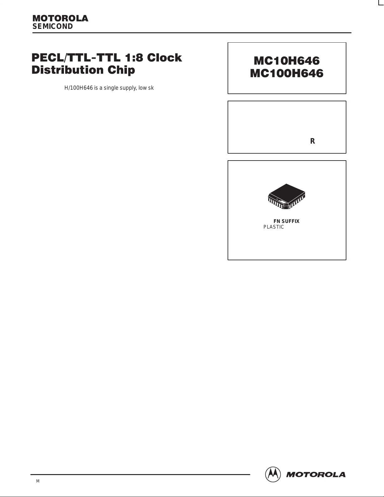
Pinout: 28–Lead PLCC
1
2
3
4
567891011
TCLK
IVT
(Top View)
VEE
IGND
VEE
OGNDQ7
18
17
16
15
14
13
12
VEE
ECLK
EN
IVT
IGND
VCCE
VCCE
VBB
ECLK
PIN NAMES
PIN FUNCTION
OGND
OVT
IGND
IVT
V
EE
V
CCE
ECLK, ECLK
V
BB
Q0–Q7
EN
INTERNAL TTL POWER
TTL Output Ground (0V)
TTL Output VCC (+5.0V)
Internal TTL GND (0V)
Internal TTL VCC (+5.0V)
ECL VEE (0V)
ECL Ground (5.0V)
Differential Signal Input
(PECL)
VBB Reference Output
Signal Outputs (TTL)
Tri–State Enable Input (TTL)
IVT01
OVT01
EN
TCLK
ECLK
ECLK
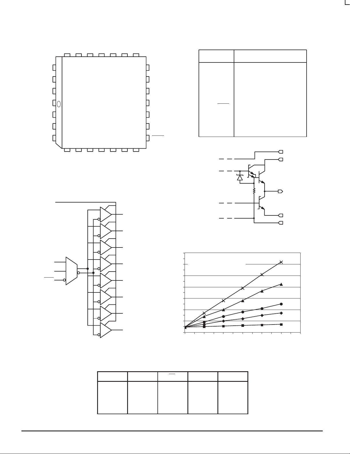
LOGIC DIAGRAM
Q0
Q1
Q2
Q3
Q4
Q5
Q6
Q7
INTERNAL TTL GROUND IGND01
Figure 1. Output Structure
700
P
600
500
400
300
POWER, mW
200
100
Dynamic
P
Total
0
0 20 40 60 80 100 120
Power versus Frequency per Bit
= CL ƒ V
Static
Swing VCC
+ P
Dynamic
FREQUENCY, MHz
= P
Figure 2. Power versus Frequency (Typical)
Q0A
OGND0
300pF
200pF
100pF
50pF
No Load
TRUTH TABLE
TCLK ECLK ECLK EN Q
GND
GND
H
L
X
L = Low Voltage Level; H = High Voltage Level; Z = Tristate
MOTOROLA TIMING SOLUTIONS
L
H
GND
GND
X
H
L
GND
GND
X
2
H
H
H
H
L
L
H
H
L
Z
BR1333 — Rev 6
 Loading...