

MOTOROLA MC10H645FN, MC10H645FNR2 Datasheet
MOTOROLA
SEMICONDUCTOR TECHNICAL DATA
1:9 TTL Clock Driver
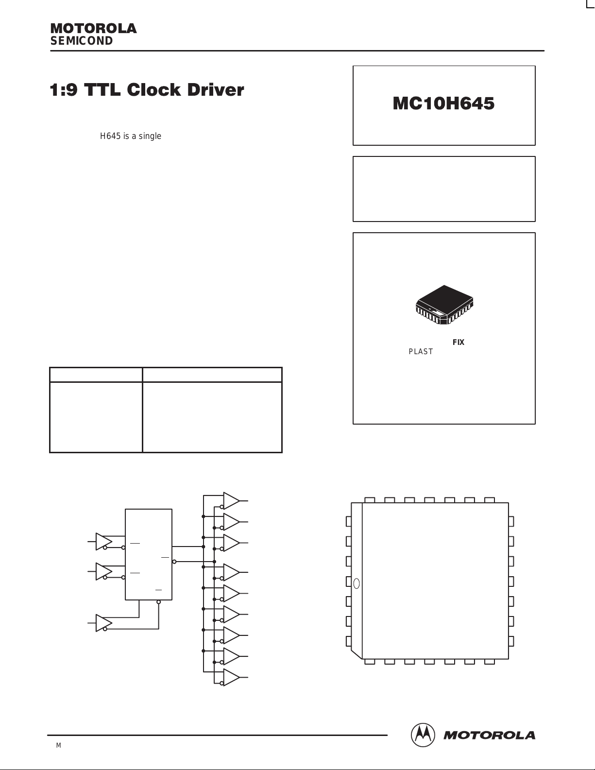
The MC10H645 is a single supply , low skew, TTL I/O 1:9 Clock Driver.
Devices in the Motorola H600 clock driver family utiize the 28–lead PLCC
for optimal power and signal pin placement.
The device features a 24mA TTL ouput stage with AC performance
specified into a 50pF load capacitance. A 2:1 input mux is provided on
chip to allow for distributing both system and diagnostic clock signals or
designing clock redundancy into a system. With the SEL input held LOW
the DO input will be selected, while the D1 input is selected when the SEL
input is forced HIGH.
• Low Skew Typically 0.65ns Within Device
• Guaranteed Skew Spec 1.25ns Part–to–Part
• Input Clock Muxing
• Differential ECL Internal Design
• Single Supply
• Extra TTL and ECL Power/Ground Pins
PIN NAMES
PIN FUNCTION
GT
VT
VE
GE
Dn
Q0 – Q8
SEL
TTL Ground (0V)
TTL VCC (+5.0V)
ECL VCC (+5.0V)
ECL Ground (0V)
TTL Signal Input
TTL Signal Outputs
TTL Mux Select
MC10H645
1:9 TTL
CLOCK DRIVER
FN SUFFIX
PLASTIC PACKAGE
CASE 776–02
TTL
Inputs
D0
D1
SEL
9/96
Motorola, Inc. 1996
LOGIC DIAGRAM
MUX
D0
D0
D1
D1
Q
Q
SS
TTL Outputs
Q0
Q1
Q2
Q3
Q4
Q5
Q6
Q7
Q8
2–1
GT
Q5
VT
Q4
VT
Q3
GT
Pinout: 28–Lead PLCC (Top View)
GT Q6 VT Q7 VT Q8 GT
25 24 23 22 21 20 19
26
27
28
1
2
3
4
567891011
GT
Q2 VT Q1 VT Q0 GT
REV 4
18
17
16
15
14
13
12
NC
D0
D1
VE
SEL
GE
NC
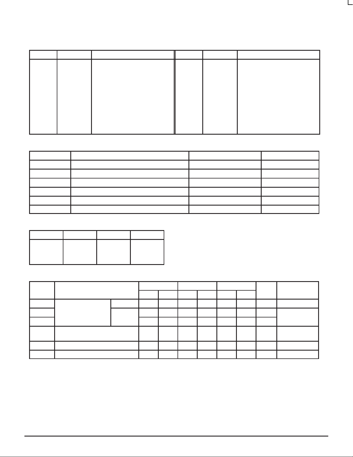
MC10H645
PIN DESCRIPTIONS
Pin Symbol Description Pin Symbol Description
1
2
3
4
5
6
7
8
9
10
11
12
13
14
ABSOLUTE RATINGS (Do not exceed)
Symbol Characteristic Value Unit
VE (ECL) Power Supply Voltage –0.5 to +7.0 V
VT (TTL) Power Supply Voltage –0.5 to +7.0 V
VI (TTL) Input Voltage –0.5 to +7.0 V
V
out
T
stg
T
amb
Q4
VT
Q3
GT
GT
Q2
VT
Q1
VT
Q0
GT
NC
GE
SEL
Signal Output (TTL)
TTL VCC (+5.0V)
Signal Output (TTL)
TTL Ground (0V)
TTL Ground (0V)
Signal Output (TTL)
TTL VCC (+5.0V)
Signal Output (TTL)
TTL VCC (+5.0V)
Signal Output (TTL)
TTL Ground (0V)
No Connection
ECL Ground
Select Input (TTL)
Disabled 3–State Output 0.0 to V
Storage Temperature –65 to 150 °C
Operating Temperature 0.0 to +85 °C
15
16
17
18
19
20
21
22
23
24
25
26
27
28
VE
D1
D0
NC
GT
Q8
VT
Q7
VT
Q6
GT
GT
Q5
VT
ECL VCC (+5.0V)
Signal Input (TTL)
Signal Input (TTL)
No Connection
TTL Ground (0V)
Signal Output (TTL)
TTL VCC (+5.0V)
Signal Output (TTL)
TTL VCC (+5.0V)
Signal Output (TTL)
TTL Ground (0V)
TTL Ground (0V)
Signal Output (TTL)
TTL VCC (+5.0V)
T
V
TRUTH TABLE
D0 D1 SEL Q
L
H
X
X
X
X
L
H
L
L
H
H
L
H
L
H
DC CHARACTERISTICS (VT = VE = 5.0V ±5%)
0°C 25°C 85°C
Symbol Characteristic Min Max Min Max Min Max Unit Condition
I
EE
I
CCH
I
CCL
V
OH
V
OL
I
OS
Power Supply Current ECL 30 30 30 mA VE Pin
TTL 30 30 30 mA Total all VT pins
35 35 35 mA
Output HIGH Voltage 2.5
2.0
Output LOW Voltage 0.5 0.5 0.5 V IOL = 24mA
Output Short Circuit Current –100 –225 –100 –225 –100 –225 mA V
2.5
2.0
2.5
2.0
V IOH = –3.0mA
IOH = –15mA
= 0V
OUT
MOTOROLA MECL Data
2–2
DL122 — Rev 6
 Loading...