

MOTOROLA
SEMICONDUCTOR TECHNICAL DATA
Differential Receiver
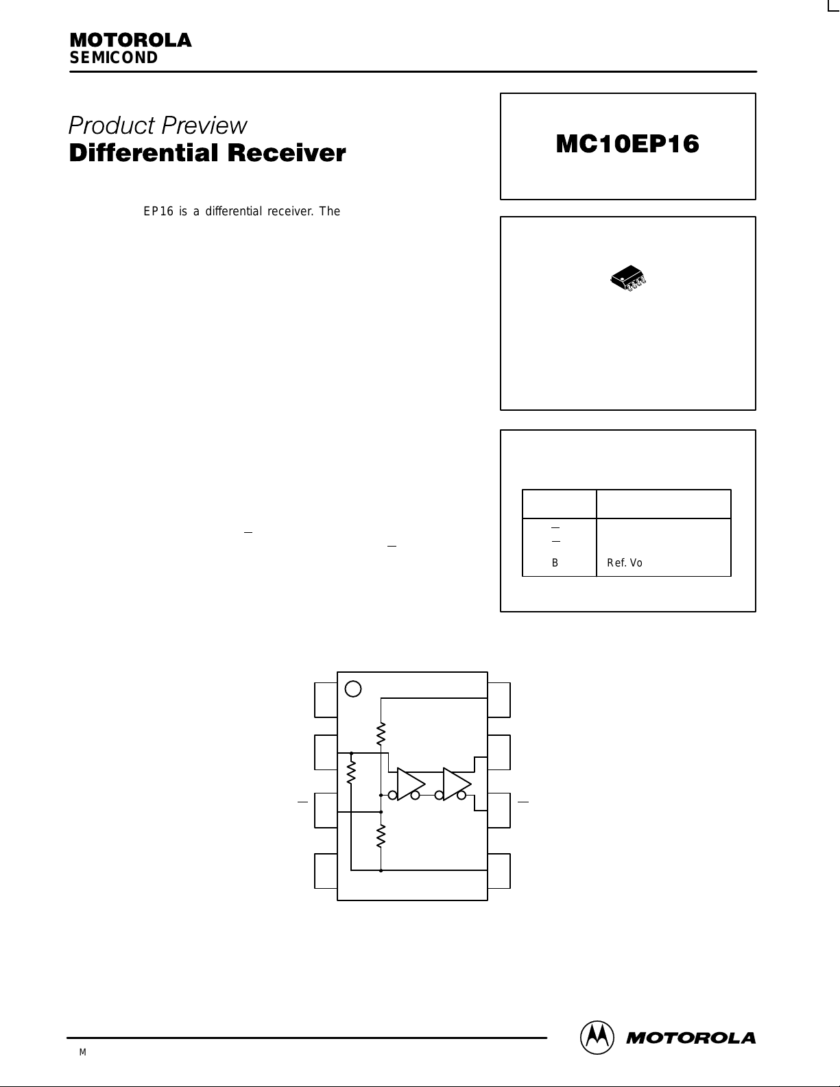
The MC10EP16 is a differential receiver. The device is functionally
equivalent to the EL16 device with higher performance capabilities. With
output transition times significantly faster than the EL16 the EP16 is
ideally suited for interfacing with high frequency sources.
The EP16 provides a VBB output for either single-ended use or as a DC
bias for AC coupling to the device. The VBB pin should be used only as a
bias for the EP16 as its current sink/source capability is limited.
Whenever used, the VBB pin should be bypassed to ground via a 0.01µf
capacitor.
Under open input conditions (pulled to VEE) internal input clamps will
force the Q output LOW.
• 160ps Propagation Delay
• High Bandwidth Output Transitions
• 75kΩ Internal Input Pulldown Resistors
• >1000V ESD Protection
• Maximum Frequency > 2.7GHz
• V
Sink/Source Current = 0.5mA maximum
BB
• Component Count = 22 NPN devices
NOTE: Inputs have 75kΩ to VEE on D input and 75kΩ to VEE and VCC on D input
and when left open, force outputs to known state Q=Low, Q
temp 265°C for maximum for < 2–3 seconds; 245°C desired.
=High. Solder
MC10EP16
8–LEAD PLASTIC SOIC PACKAGE
PIN FUNCTION
D, D
Q, Q
V
BB Ref. Voltage Output
D SUFFIX
CASE 751-06
PIN DESCRIPTION
Data Inputs
Data Outputs
1
NC
75k
2
D
75k
D
3
75k
V
Figure 1. 8–Lead Pinout (Top View) and Logic Diagram
This document contains information on a product under development. Motorola reserves the right to change or
discontinue this product without notice.
3/98
Motorola, Inc. 1998
45
BB
1
8
V
7
Q
6
Q
V
REV 0
CC
EE
MC10EP16
MAXIMUM RATINGS*
Symbol Parameter Value Unit
V
EE
V
I
I
out
T
A
V
EE
θ
JA
θ
JC
* Maximum Ratings are those values beyond which damage to the device may occur. Functional operation should be restricted to the
Recommended Operating Conditions.
Power Supply (VCC = 0V) –8.0 to +0 VDC
Input Voltage (VCC = 0V) 0 to +–6.0 VDC
Output Current Continuous
Surge
50
100
mA
Operating Temperature Range –40 to +85 °C
Operating Range –5.5 to 3.0 V
Thermal Resistance (Junction–to–Ambient) Still Air
500lfpm
190
130
°C/W
Thermal Resistance (Junction–to–Case) 41 to 44 (±5%) °C/W
DC CHARACTERISTICS (VEE = VEE(min) to VEE(max); VCC =
–40°C 0°C 25°C 85°C
Symbol Characteristic Min Typ Max Min Typ Max Min Typ Max Min Typ Max Unit
V
V
V
V
V
V
I
IH
I
IL
IEE
Output HIGH Voltage –1080 –890 –1020 –840 –980 –810 –910 –720 mV
OH
Output LOW Voltage –1950 –1650 –1950 –1630 –1950 –1630 –1950 –1595 mV
OL
Input HIGH Voltage –1230 –890 –1170 –840 –1130 –810 –1060 –720 mV
IH
Input LOW Voltage –1950 –1500 –1950 –1480 –1950 –1480 –1950 –1445 mV
IL
Power Supply Voltage –5.5 –3.0 –5.5 –3.0 –5.5 –3.0 –5.5 –3.0 Volts
EE
Reference Voltage mV
BB
Input HIGH Current 150 150 150 150 µA
Input LOW Current DD0.5
–600
VEE Supply Current 23 29 23 29 23 29 23 29 mA
0.5
–600
GND; Note 1.)
0.5
–600
0.5
–600
µA
µA
1. 10EL circuits are designed to meet the DC specifications shown in the table after thermal equilibrium has been established. The circuit is in
a test socket or mounted on a printed circuit board and transverse airflow greater than 500lfpm is maintained. Outputs are terminated through
a 50Ω resistor to VCC –2.0V except where otherwise specified on the individual data sheets.
AC CHARACTERISTICS (VEE = VEE(min) to VEE(max); VCC = GND)
–40°C 0°C 25°C 85°C
Symbol Characteristic Min Typ Max Min Typ Max Min Typ Max Min Typ Max Unit
f
max
t
PLH
t
PHL
t
SKEW
V
V
t
r
t
f
2. Minimum f
3. Duty cycle skew is the difference between a T
4. Minimum input swing for which AC parameters guaranteed. The device has a DC gain of ≈40.
5. The CMR range is referenced to the most positive side of the differential input signal. Normal operation is obtained if the HIGH level falls within
Maximum Frequency (Note 2.) 2.7 2.7 2.7 2.7 GHz
,
Propagation Delay to Output Diff. 160 160 160 160 ps
Duty Cycle Skew (Note 3.) Diff. 5.0 5.0 20 5.0 20 5.0 20 ps
Minimum Input Swing (Note 4.) 150 150 150 150 mV
PP
Common Mode Range (Note 5.) –0.4 –0.4 –0.4 –0.4 V
CMR
Output Rise/Fall Times Q
(20% – 80%)
specified to 2.7GHz with reduced output swing. See Figure 2 on page 3.
max
110 110 110 110 ps
PLH
and T
propagation delay through a device.
PHL
the specified range and the peak-to-peak voltage lies between VPPmin and 1V . The lower end of the CMR range is dependent on VEE and is
equal to VEE + 2.5V.
MOTOROLA ECLinPS and ECLinPS Lite
2
DL140 — Rev 3
 Loading...