

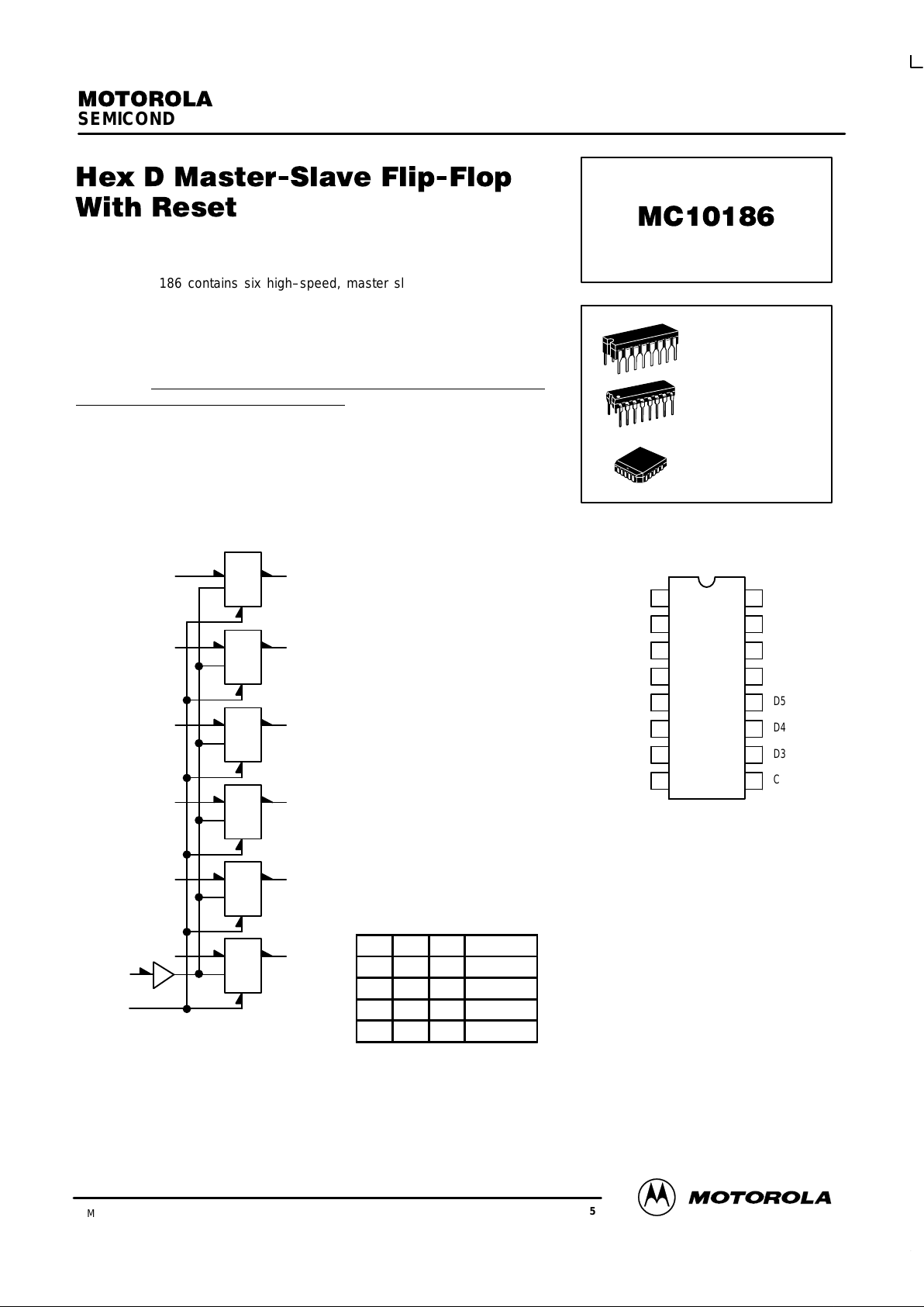
LOGIC DIAGRAM
VCC= PIN 16
VEE= PIN 8
2 5
CLOCK
RESET 1
9
Q0
3 Q1
4 Q2
13 Q3
14 Q4
15 Q5
D0
6D1
7D2
10D3
11D4
D5
12
SEMICONDUCTOR TECHNICAL DATA
3–147
REV 5
Motorola, Inc. 1996
3/93
The MC10186 contains six high–speed, master slave type “D” flip–flops.
Clocking is common to all six flip–flops. Data is entered into the master when
the clock is low. Master to slave data transfer takes place on the positive–going
Clock transition. Thus, outputs may change only on a positive–going Clock
transition. A change in the information present at the data (D) input will not affect
the output information any other time due to the master–slave construction of
this device. A COMMON RESET IS INCLUDED IN THIS CIRCUIT. RESET
ONLY FUNCTIONS WHEN CLOCK IS LOW.
PD= 460 mW typ/pkg (No Load)
f
toggle
= 150 MHz (typ)
tr, tf= 2.0 ns typ (20%–80%)
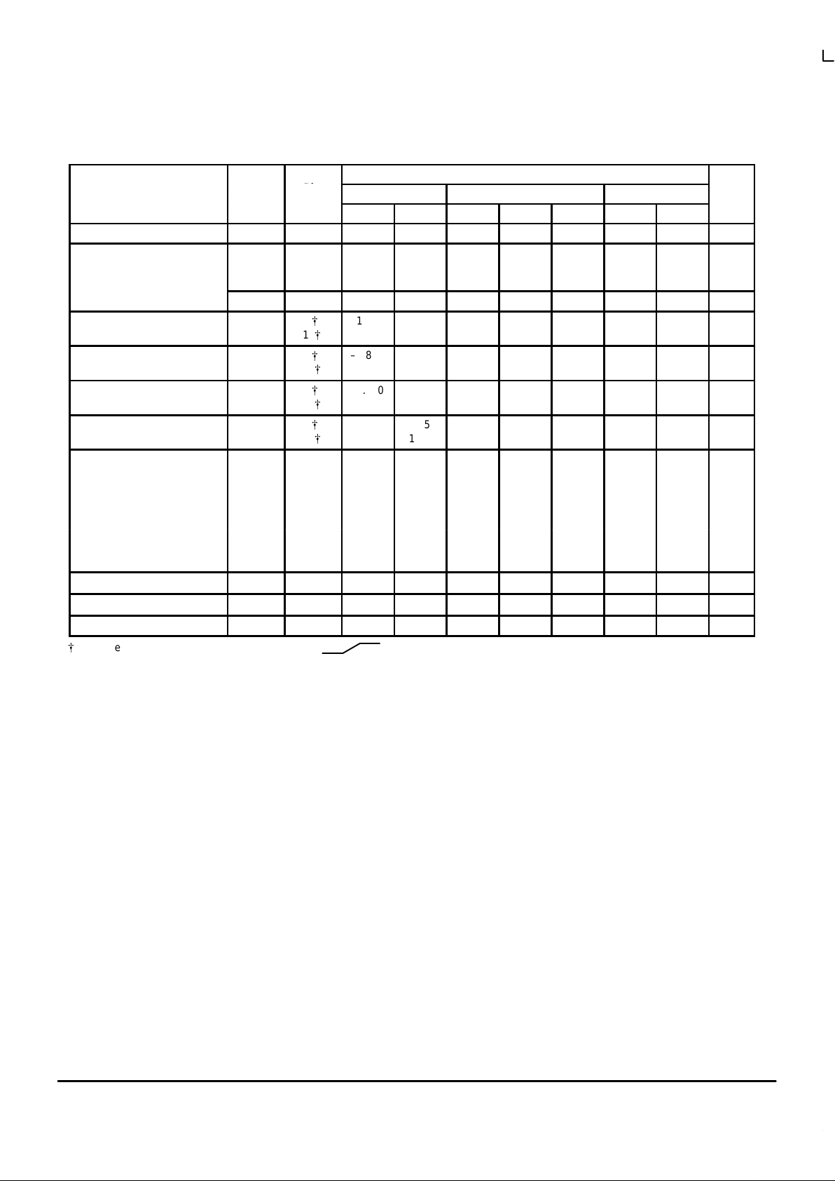
CLOCKED TRUTH TABLE
R C D Qn + 1
L L X Q
n
L H* L L
L H* H H
H L X L
*A clock H is a clock transition
from a low to a high state.
DIP
PIN ASSIGNMENT
RESET
Q0
Q1
Q2
D0
D1
D2
V
EE
V
CC
Q5
Q4
Q3
D5
D4
D3
CLOCK
16
15
14
13
12
11
10
9
1
2
3
4
5
6
7
8
Pin assignment is for Dual–in–Line Package.
For PLCC pin assignment, see the Pin Conversion
T ables on page 6–11 of the Motorola MECL Data
Book (DL122/D).
L SUFFIX
CERAMIC PACKAGE
CASE 620–10
P SUFFIX
PLASTIC PACKAGE
CASE 648–08
FN SUFFIX
PLCC
CASE 775–02
MC10186
MOTOROLA MECL Data
DL122 — Rev 6
3–148
ELECTRICAL CHARACTERISTICS
Test Limits
Pin
Under
–30°C +25°C +85°C
Characteristic Symbol
Under
Test
Min Max Min Typ Max Min Max
Unit
Power Supply Drain Current I
E
8 121 88 110 121 mAdc
Input Current I
inH
5
9
1
350
495
920
220
310
575
220
310
575
µAdc
I
inL
5 0.5 0.5 0.3 µAdc
Output Voltage Logic 1 V
OH
2
[
15
[
–1.060
–1.060
–0.890
–0.890
–0.960
–0.960
–0.810
–0.810
–0.890
–0.890
–0.700
–0.700
Vdc
Output Voltage Logic 0 V
OL
2
[
15
[
–1.890
–1.890
–1.675
–1.675
–1.850
–1.850
–1.650
–1.650
–1.825
–1.825
–1.615
–1.615
Vdc
Threshold Voltage Logic 1 V
OHA
2
[
15
[
–1.080
–1.080
–0.980
–0.980
–0.910
–0.910
Vdc
Threshold Voltage Logic 0 V
OLA
2
[
15
[
–1.655
–1.655
–1.630
–1.630
–1.595
–1.595
Vdc
Switching Times (50Ω Load) ns
Propagation Delay t
1+3–
t
1+4–
t
9+2+
t
9+2–
3
4
2
2
1.6
1.6
1.6
1.6
4.6
4.6
4.6
4.6
1.6
1.6
1.6
1.6
2.5
2.5
3.5
3.5
4.5
4.5
4.5
4.5
1.6
1.6
1.6
1.6
5.0
5.0
5.0
5.0
Rise Time (20 to 80%) t
2+
2 1.0 4.1 1.1 1.8 4.0 1.1 4.4
Fall Time (20 to 80%) t
2–
2 1.0 4.1 1.1 1.8 4.0 1.1 4.4
Setup Time t
setup
2 2.5 2.5 2.5 2.5 ns
Hold Time t
hold
2 1.5 1.5 –1.5 1.5 ns
Toggle Frequency (Max) f
tog
2 125 125 150 125 MHz
[
Output level to be measured after clock pulse.
V
IH
V
IL
appears at clock input (Pin 9).
 Loading...