

SEMICONDUCTOR TECHNICAL DATA
3–141
REV 6
Motorola, Inc. 1996
9/96
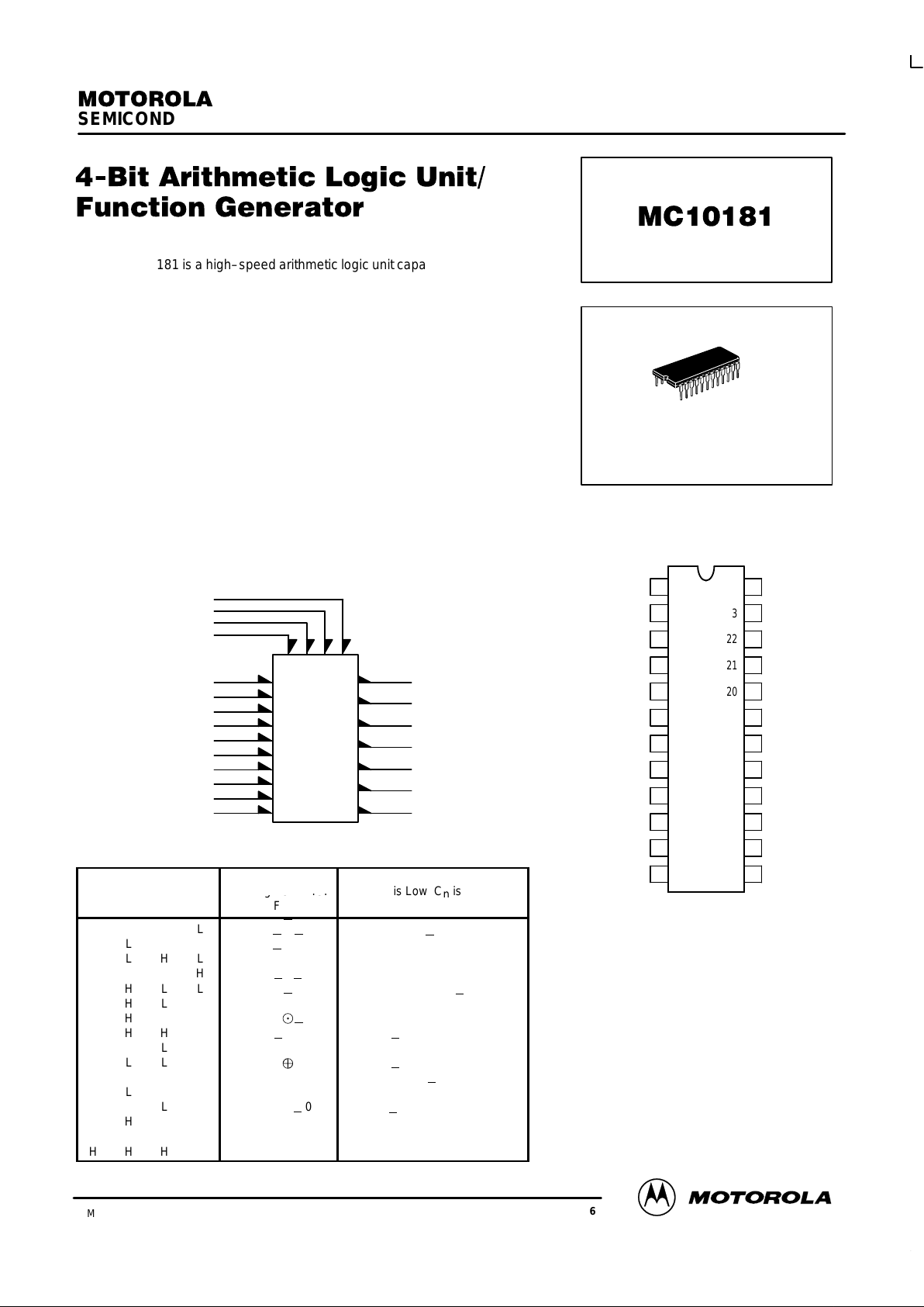
The MC10181 is a high–speed arithmetic logic unit capable of performing 16
logic operations and 16 arithmetic operations on two four–bit words. Full
internal carry is incorporated for ripple through operation.
Arithmetic logic operations are selected by applying the appropriate binary
word to the select inputs (S0 through S3) as indicated in the tables of
arithmetic/logic functions. Group carry propagate (PG) and carry generate (GG)
are provided to allow fast operations on very long words using a second order
look ahead. The internal carry is enabled by applying a low level voltage to the
mode control input (M).
PD= 600 mW typ/pkg (No Load)
tpd (typ): A1 to F = 6.5 ns
Cn to Cn + 4 = 3.1 ns
A1 to PG = 5.0 ns
A1 to GG = 4.5 ns
A1 to Cn + 4 = 5.0
LOGIC DIAGRAM
V
CC1
= PIN 1
V
CC2
= PIN 24
VEE= PIN 12
23
13
15
17
14
21
20
18
19
16
11
10
9
22
2
3
7
6
4
8
5
S0 S1 S2 S3
A0
B0
A1
B1
A2
B2
A3
B3
C
n
M
F0
F1
F2
F3
G
G
P
G
C
n+4
Logic Functions Arithmetic Operation
Function Select
Logic Functions
M is High C = D.C.
Arithmetic Operation
M is Low C
is low
S3 S2 S1 S0
M is High C = D.C
.
F
M is Low C
n
is
low
F
L
L
L
L
L
L
L
L
H
H
H
H
H
H
H
H
L
L
L
L
H
H
H
H
L
L
L
L
H
H
H
H
L
L
H
H
L
L
H
H
L
L
H
H
L
L
H
H
L
H
L
H
L
H
L
H
L
H
L
H
L
H
L
H
F = A
F = A + B
F = A + B
F = Logical “1”
F = A • B
F = B
F = AB
F = A + B
F = A • B
F = A B
F = B
F = A + B
F = Logical “0”
F = A
• B
F = A • B
F = A
F = A
F = A plus (A • B)
F = A plus (A • B)
F = A times 2
F = (A + B) plus 0
F = (A + B) plus (A
• B)
F = A plus B
F = A plus (A + B)
F = (A + B) plus 0
F = A minus B minus 1
F = (A + B) plus (A • B)
F = A plus (A + B)
F = minus 1 (two’s complement)
F = (A
• B) minus 1
F = (A • B) minus 1
F = A minus 1
PIN ASSIGNMENT
V
CC1
F0
F1
G
G
CN +
4
F3
F2
P
G
V
CC2
M
C
N
A0
B0
B1
A1
S1
24
23
22
21
20
19
18
17
1
2
3
4
5
6
7
8
B3
A3
B2
V
EE
A2
S2
S0
S3
16
15
14
13
9
10
11
12
L SUFFIX
CERAMIC PACKAGE
CASE 623–05

MC10181
MOTOROLA MECL Data
DL122 — Rev 6
3–142
S3 13
S2 15
S1 17
S0 14
B0 20
A0 21
B1 19
A1 18
B2 11
A2 16
B3 9
A3 10
Cn 22
M 23
2 F0
3 F1
7 F2
6 F3
8 P
G
4 G
G
5 C
n+4
POSITIVE LOGIC DIAGRAM

MC10181
3–143 MOTOROLAMECL Data
DL122 — Rev 6
ELECTRICAL CHARACTERISTICS
Test Limits
Pin
Under
–30°C +25°C +85°C
Characteristic Symbol
Under
Test
Min Max Min Typ Max Min Max
Unit
Power Supply Drain Current I
E
12 159 145 159 mAdc
Input Current I
inH
9
10
11
13
14
15
16
17
18
19
20
21
22
23
390
350
390
320
425
425
350
425
350
390
390
350
460
320
245
220
245
200
265
265
220
265
220
245
245
220
290
200
245
220
245
200
265
265
220
265
220
245
245
220
290
200
µAdc
Input Leakage Current I
inL
9
10
11
13
14
15
16
17
18
19
20
21
22
23
0.5
0.5
0.5
0.5
0.5
0.5
0.5
0.5
0.5
0.5
0.5
0.5
0.5
0.5
0.5
0.5
0.5
0.5
0.5
0.5
0.5
0.5
0.5
0.5
0.5
0.5
0.5
0.5
0.3
0.3
0.3
0.3
0.3
0.3
0.3
0.3
0.3
0.3
0.3
0.3
0.3
0.3
µAdc
Output Voltage Logic 1 V
OH
* –1.060 –0.890 –0.960 –0.810 –0.890 –0.700 Vdc
Output Voltage Logic 0 V
OL
* –2.000 –1.675 –1.990 –1.650 –1.920 –1.615 Vdc
Threshold Voltage Logic 1 V
OHA
* –1.080 –0.980 –0.910 Vdc
Threshold Voltage Logic 0 V
OLA
* –1.655 –1.630 –1.595 Vdc
* Test all input–output combinations according to Function Table.
** For threshold level test, apply threshold input level to only one input pin at a time.

MC10181
MOTOROLA MECL Data
DL122 — Rev 6
3–144
ELECTRICAL CHARACTERISTICS (continued)
TEST VOLTAGE VALUES (Volts)
@ Test Temperature V
IHmax
V
ILmin
V
IHAminVILAmax
V
EE
–30°C –0.890 –1.890 –1.205 –1.500 –5.2
+25°C –0.810 –1.850 –1.105 –1.475 –5.2
+85°C –0.700 –1.825 –1.035 –1.440 –5.2
Pin
TEST VOLTAGE APPLIED TO PINS LISTED BELOW
Characteristic Symbol
Und
er
Test
V
IHmax
V
ILmin
V
IHAminVILAmax
V
EE
(VCC)
Gnd
Power Supply Drain Current I
E
12 12 1, 24
Input Current I
inH
9
10
11
13
14
15
16
17
18
19
20
21
22
23
9
10
11
13
14
15
16
17
18
19
20
21
22
23
12
12
12
12
12
12
12
12
12
12
12
12
12
12
1, 24
1, 24
1, 24
1, 24
1, 24
1, 24
1, 24
1, 24
1, 24
1, 24
1, 24
1, 24
1, 24
1, 24
Input Leakage Current I
inL
9
10
11
13
14
15
16
17
18
19
20
21
22
23
9
10
11
13
14
15
16
17
18
19
20
21
22
23
12
12
12
12
12
12
12
12
12
12
12
12
12
12
1, 24
1, 24
1, 24
1, 24
1, 24
1, 24
1, 24
1, 24
1, 24
1, 24
1, 24
1, 24
1, 24
1, 24
Output Voltage Logic 1 V
OH
* * * 12 1, 24
Output Voltage Logic 0 V
OL
* * * 12 1, 24
Threshold Voltage Logic 1 V
OHA
* ** ** 12 1, 24
Threshold Voltage Logic 0 V
OLA
* ** ** 12 1, 24
* Test all input–output combinations according to Function Table.
** For threshold level test, apply threshold input level to only one input pin at a time.
Each MECL 10,000 series circuit has been designed to meet the dc specifications shown in the test table, after thermal equilibrium has been
established. The circuit is in a test socket or mounted on a printed circuit board and transverse air flow greater than 500 linear fpm is maintained.
Outputs are terminated through a 50–ohm resistor to –2.0 volts. Test procedures are shown for only one gate. The other gates are tested in the
same manner.

MC10181
3–145 MOTOROLAMECL Data
DL122 — Rev 6
AC Switching Characteristics
–30°C * +25°C +85°C *
Characteristic Symbol Input Output Conditions†Min Max Min Typ Max Min Max Unit
Propagation Delay
Rise Time, Fall Time
t++,t– –
t+,t–
C
n
C
n
C
n+4
C
n+4
A0,A1,A2,A3
A0,A1,A2,A3
1.0
1.0
5.1
3.2
1.1
1.0
3.1
2.0
5.0
3.0
1.1
1.0
5.4
3.2nsns
Propagation Delay
Rise Time, Fall Time
t++,t+–
t–+,t– –
t+,t–
C
n
C
n
C
n
F1
F1
F1
A0
A0
A0
1.7
1.7
1.3
7.2
7.2
5.3
2.0
2.0
1.5
4.5
4.5
3.0
7.0
7.0
5.0
2.0
2.0
1.5
7.5
7.5
5.3
ns
ns
ns
Propagation Delay
Rise Time, Fall Time
t++,t+–
t–+,t– –
t+,t–
A1
A1
A1
F1
F1
F1
—
—
—
2.6
2.6
1.3
10.4
10.4
5.4
3.0
3.0
1.5
6.5
6.5
3.0
10
10
5.0
3.0
3.0
1.5
10.8
10.8
5.3
ns
ns
ns
Propagation Delay
Rise Time, Fall Time
t++,t– –
t+,t–
A1
A1
P
G
P
G
S0,S3
S0,S3
1.6
0.8
7.0
3.7
2.0
1.1
5.0
2.0
6.5
3.5
2.0
1.1
7.0
3.8nsns
Propagation Delay
Rise Time, Fall Time
t++,t– –
t+,t–
A1
A1
G
G
G
G
A0,A2,A3,C
n
A0,A2,A3,C
n
1.1
1.2
7.4
5.1
2.0
1.5
4.5
4.0
7.0
5.0
1.3
1.2
7.7
5.3nsns
Propagation Delay
Rise Time, Fall Time
t+–,t–+
t+,t–
A1A1C
n+4
C
n+4
A0,A2,A3,C
n
A0,A2,A3,C
n
1.7
1.0
7.3
3.1
2.0
1.0
5.0
2.0
7.0
3.0
2.0
1.0
7.8
3.2nsns
Propagation Delay
Rise Time, Fall Time
t++,t–+
t+,t–
B1
B1
F1
F1
S3,C
n
S3,C
n
2.7
1.2
11.3
5.3
3.0
1.5
8.0
3.5115.0
3.0
1.5
11.9
5.3nsns
Propagation Delay
Rise Time, Fall Time
t++,t– –
t+,t–
B1
B1
P
G
P
G
S0,A1
S0,A1
1.6
1.0
7.7
3.6
2.0
1.1
6.0
2.0
7.5
3.5
2.0
1.1
8.0
3.9nsns
Propagation Delay
Rise Time, Fall Time
t++,t– –
t+,t–
B1
B1
G
G
G
G
S3,C
n
S3,C
n
1.7
1.4
8.2
5.2
2.0
1.5
6.0
3.0
8.0
5.0
2.0
1.2
8.6
5.4nsns
Propagation Delay
Rise Time, Fall Time
t+–,t–+
t+,t–
B1B1C
n+4
C
n+4
S3,C
n
S3,C
n
1.8
0.9
8.2
3.1
2.0
1.0
6.0
2.0
8.0
3.0
2.0
1.0
8.7
3.2nsns
Propagation Delay
Rise Time, Fall Time
t++,t+–
t+,t–
M
M
F1
F1
—
—
2.4
1.1
10.3
5.1
3.0
1.5
6.5
4.0105.0
3.0
1.5
10.8
5.3nsns
Propagation Delay
Rise Time, Fall Time
t+–,t–+
t+,t–
S1
S1
F1
F1
A1,B1
A1,B1
2.5
1.0
10.7
5.4
3.0
1.5
6.5
3.0105.0
3.0
1.5
10.8
5.4nsns
Propagation Delay
Rise Time, Fall Time
t–+,t+–
t+,t–
S1
S1
P
G
P
G
A3,B3
A3,B3
1.7
0.8
8.3
5.1
2.0
1.1
6.0
3.0
8.0
5.0
2.0
1.1
8.4
5.2nsns
Propagation Delay
Rise Time, Fall Time
t+–,t–+
t+,t–
S1S1C
n+4
C
n+4
A3,B3
A3,B3
1.6
0.9
9.3
5.3
2.0
1.1
6.0
3.0
9.0
5.0
2.0
1.0
9.9
5.2nsns
Propagation Delay
Rise Time, Fall Time
t+–,t–+
t+,t–
S1
S1
G
G
G
G
A3,B3
A3,B3
1.5
0.8
9.6
6.2
2.0
0.8
6.0
3.0
9.0
6.0
1.9
0.8
9.7
6.5nsns
†Logic high level (+1.11 Vdc) applied to pins listed. All other
input pins are left floating or tied to +0.31 Vdc.
V
CC1
= V
CC2
= +2.0 Vdc, VEE = –3.2 Vdc
* L Suffix Only

MC10181
MOTOROLA MECL Data
DL122 — Rev 6
3–146
OUTLINE DIMENSIONS
L SUFFIX
CERAMIC PACKAGE
CASE 623–05
ISSUE M
NOTES:
1. DIMENSION L TO CENTER OF LEADS WHEN
FORMED PARALLEL.
2. LEADS WITHIN 0.13 (0.005) RADIUS OF TRUE
POSITION AT SEATING PLANE AT MAXIMUM
MATERIAL CONDITION (WHEN FORMED
PARALLEL).
112
24 13
B
A
SEATING
PLANE
F
D
G
K
N
C
M
J
L
DIM MIN MAX MIN MAX
INCHESMILLIMETERS
A 31.24 32.77 1.230 1.290
B 12.70 15.49 0.500 0.610
C 4.06 5.59 0.160 0.220
D 0.41 0.51 0.016 0.020
F 1.27 1.52 0.050 0.060
G 2.54 BSC 0.100 BSC
J 0.20 0.30 0.008 0.012
K 3.18 4.06 0.125 0.160
L 15.24 BSC 0.600 BSC
M 0 15 0 15
N 0.51 1.27 0.020 0.050
____
Motorola reserves the right to make changes without further notice to any products herein. Motorola makes no warranty , representation or guarantee regarding
the suitability of its products for any particular purpose, nor does Motorola assume any liability arising out of the application or use of any product or circuit, and
specifically disclaims any and all liability, including without limitation consequential or incidental damages. “T ypical” parameters which may be provided in Motorola
data sheets and/or specifications can and do vary in different applications and actual performance may vary over time. All operating parameters, including “Typicals”
must be validated for each customer application by customer’s technical experts. Motorola does not convey any license under its patent rights nor the rights of
others. Motorola products are not designed, intended, or authorized for use as components in systems intended for surgical implant into the body, or other
applications intended to support or sustain life, or for any other application in which the failure of the Motorola product could create a situation where personal injury
or death may occur. Should Buyer purchase or use Motorola products for any such unintended or unauthorized application, Buyer shall indemnify and hold Motorola
and its officers, employees, subsidiaries, affiliates, and distributors harmless against all claims, costs, damages, and expenses, and reasonable attorney fees
arising out of, directly or indirectly, any claim of personal injury or death associated with such unintended or unauthorized use, even if such claim alleges that
Motorola was negligent regarding the design or manufacture of the part. Motorola and are registered trademarks of Motorola, Inc. Motorola, Inc. is an Equal
Opportunity/Affirmative Action Employer.
How to reach us:
USA/EUROPE/Locations Not Listed: Motorola Literature Distribution; JAPAN: Nippon Motorola Ltd.; Tatsumi–SPD–JLDC, 6F Seibu–Butsuryu–Center,
P.O. Box 5405, Denver, Colorado 80217. 303–675–2140 or 1–800–441–2447 3–14–2 Tatsumi Koto–Ku, Tokyo 135, Japan. 81–3–3521–8315
Mfax: RMFAX0@email.sps.mot.com – TOUCHT ONE 602–244–6609 ASIA/PACIFIC: Motorola Semiconductors H.K. Ltd.; 8B Tai Ping Industrial Park,
INTERNET: http://Design–NET.com 51 Ting Kok Road, Tai Po, N.T., Hong Kong. 852–26629298
MC10181/D
*MC10181/D*
◊
 Loading...