

MOTOROLA MC10104P, MC10104FNR2 Datasheet
SEMICONDUCTOR TECHNICAL DATA
3–16
REV 5
Motorola, Inc. 1996
3/93
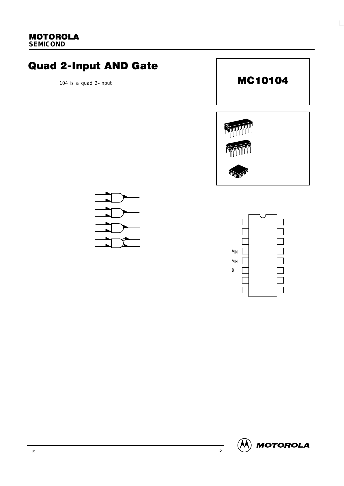
The MC10104 is a quad 2–input AND gate. One of the gates has both
AND/NAND outputs available.
PD= 35 mW typ/gate (No Load)
tpd= 2.7 ns typ
tr, tf= 2.0 ns typ (20%–80%)
LOGIC DIAGRAM
V
CC1
= PIN 1
V
CC2
= PIN 16
VEE= PIN 8
14
13
12
11
10
3
7
6
2
5
4
9
15
DIP
PIN ASSIGNMENT
V
CC1
A
OUT
B
OUT
A
IN
A
IN
B
IN
B
IN
V
EE
V
CC2
D
OUT
C
OUT
D
IN
D
IN
C
IN
C
IN
D
OUT
16
15
14
13
12
11
10
9
1
2
3
4
5
6
7
8
Pin assignment is for Dual–in–Line Package.
For PLCC pin assignment, see the Pin Conversion
T ables on page 6–11 of the Motorola MECL Data
Book (DL122/D).
L SUFFIX
CERAMIC PACKAGE
CASE 620–10
P SUFFIX
PLASTIC PACKAGE
CASE 648–08
FN SUFFIX
PLCC
CASE 775–02
MC10104
3–17 MOTOROLAMECL Data
DL122 — Rev 6
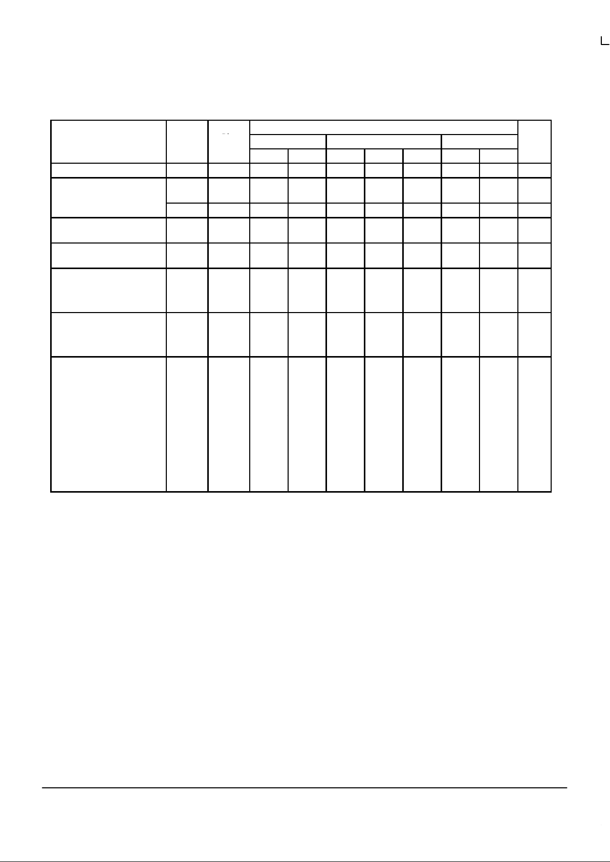
ELECTRICAL CHARACTERISTICS
Test Limits
Pin
Under
–30°C +25°C +85°C
Characteristic Symbol
Under
Test
Min Max Min Typ Max Min Max
Unit
Power Supply Drain Current I
E
8 39 35 39 mAdc
Input Current I
inH
* 12
13
425
350
265
220
265
220
µAdc
I
inL
12 0.5 0.5 0.3 µAdc
Output Voltage Logic 1 V
OH
15
9
–1.060
–1.060
–0.890
–0.890
–0.960
–0.960
–0.810
–0.810
–0.890
–0.890
–0.700
–0.700
Vdc
Output Voltage Logic 0 V
OL
15
9
–1.890
–1.890
–1.675
–1.675
–1.850
–1.850
–1.650
–1.650
–1.825
–1.825
–1.615
–1.615
Vdc
Threshold Voltage Logic 1 V
OHA
9
9
15
15
–1.090
–1.090
–1.090
–1.090
–0.980
–0.980
–0.980
–0.980
–0.910
–0.910
–0.910
–0.910
Vdc
Threshold Voltage Logic 0 V
OLA
9
9
15
15
–1.655
–1.655
–1.655
–1.655
–1.630
–1.630
–1.630
–1.630
–1.595
–1.595
–1.595
–1.595
Vdc
Switching Times (50Ω Load) ns
Propagation Delay t
12+15+
t
12–15–
t
12+9–
t
12–9+
15
15
9
9
1.0
1.0
1.0
1.0
4.3
4.3
4.3
4.3
1.0
1.0
1.0
1.0
2.2
2.2
2.2
2.2
4.0
4.0
4.0
4.0
1.0
1.0
1.0
1.0
4.2
4.2
4.2
4.2
t
13+15+
t
13+9–
15
9
1.0
1.0
4.3
4.3
1.0
1.0
2.7
2.7
4.0
4.0
1.0
1.0
4.2
4.2
Rise Time (20 to 80%) t
15+
t
9+
15
9
1.5
1.5
3.7
3.7
1.5
1.5
2.0
2.0
3.5
3.5
1.5
1.5
3.6
3.6
Fall Time (20 to 80%) t
15–
t
9–
15
9
1.5
1.5
3.7
3.7
1.5
1.5
2.0
2.0
3.5
3.5
1.5
1.5
3.6
3.6
* Inputs 4, 7, 10 and 13 will behave similarly for ac and I
inH
values.
Inputs 5, 6, 11 and 12 will behave similarly for ac and I
inH
values.
 Loading...