

MOTOROLA MC10H643FNR2, MC100H643FNR2 Datasheet
MOTOROLA
SEMICONDUCTOR TECHNICAL DATA
Dual Supply
ECL-TTL 1:8 Clock Driver
The MC10H/100H643 is a dual supply, low skew translating 1:8 clock
driver. Devices in the Motorola H600 translator series utilize the 28–lead
PLCC for optimal power pinning, signal flow through and electrical
performance. The dual–supply H643 is similar to the H641, which is a
single–supply 1:9 version of the same function.
The device features a 48mA TTL output stage, with AC performance
specified into a 50pF load capacitance. A Latch is provided on–chip.
When LEN is LOW (or left open, in which case it is pulled LOW by the
internal pulldowns) the latch is transparent. A HIGH on the enable pin
(EN
) forces all outputs LOW.
The 10H version is compatible with MECL 10H ECL logic levels. The
100H version is compatible with 100K levels.
• ECL/TTL Version of Popular ECLinPS E111
• Low Skew Within Device 0.5ns
• Guaranteed Skew Spec Part–to–Part 1.0ns
• Latch
• Differential Internal Design
• V
Output
BB
• Dual Supply
• Reset/Enable
• Multiple TTL and ECL Power/Ground Pins
MC10H643
MC100H643
DUAL SUPPLY
ECL–TTL 1:8
CLOCK DRIVER
FN SUFFIX
PLASTIC PACKAGE
CASE 776–02
Pinout: 28–Lead PLCC (Top View)
Q4
25 24 23 22 21 20 19
Q3
26
OGND2
OVT1
OGND1
ECLinPS and MECL 10H are trademarks of Motorola, Inc.
11/93
Q2
Q1
Q0
27
28
1
2
3
4
567891011
IVT1
Motorola, Inc. 1996
Q5
OGND3
V
IGND1
EE
OVT2
VEEV
2–1
Q6
EE
Q7
OGND4
D
EN
18
17
16
15
14
13
12
IVT2
IGND2
V
CCE
V
CCE
LEN
V
BB
D
PIN NAMES
PIN FUNCTION
OGND
OVT
IGND
IVT
V
EE
V
CCE
D, D
V
BB
Q0–Q7
EN
LEN
REV 3
TTL Output Ground (0V)
TTL Output VCC (+5.0V)
Internal TTL GND (0V)
Internal TTL VCC (+5.0V)
ECL VEE (–5.2/–4.5V)
ECL Ground (0V)
Signal Input (ECL)
VBB Reference Output
Signal Outputs (TTL)
Enable Input (ECL)
Latch Enable Input (ECL)
MC10H643 MC100H643
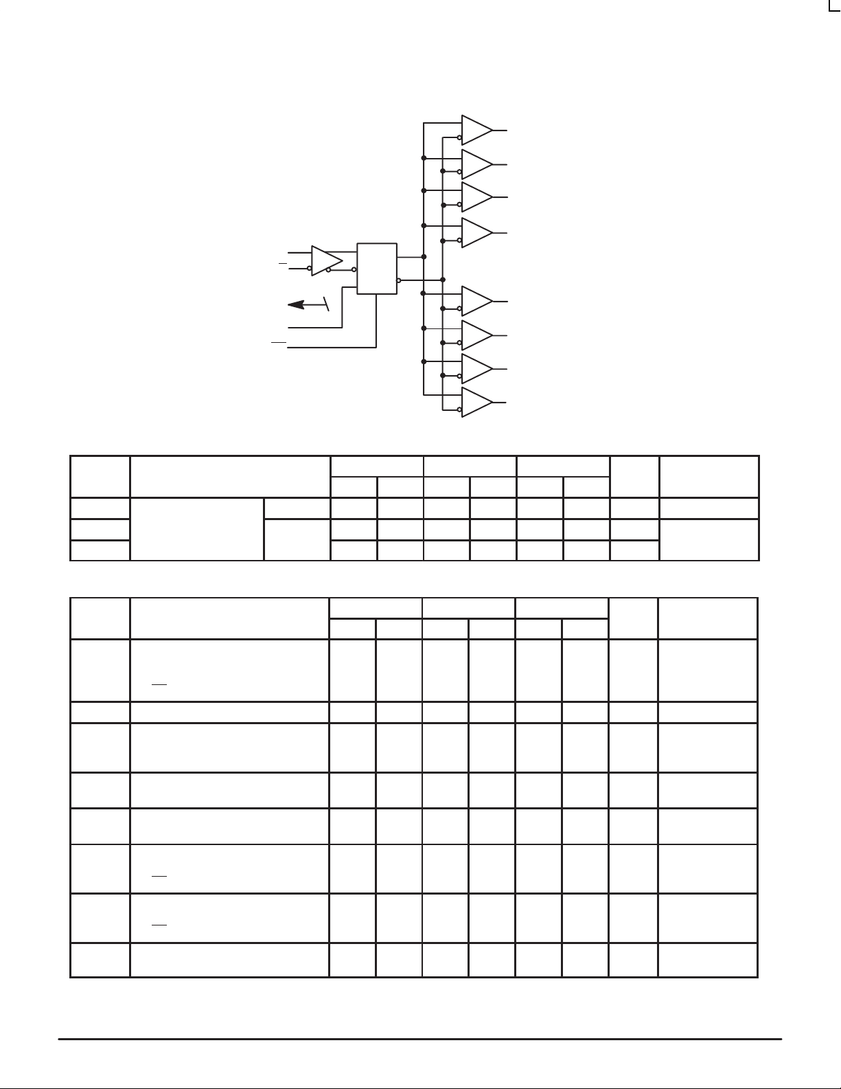
ECL INPUT
D
D
LOGIC DIAGRAM
D
Q
Q0
Q1
Q2
Q3
TTL OUTPUTS
V
BB
LEN
EN
Q4
Q5
Q6
Q7
DC CHARACTERISTICS (IVT = OVT = 5.0V ±5%; VEE = –5.2V ±5% (10H Version); VEE = –4.5V ±0.3V (100H Version))
0°C 25°C 85°C
Symbol Characteristic Min Max Min Max Min Max Unit Condition
I
EE
I
CCL
I
CCH
Power Supply Current TTL – 106 – 106 – 106 mA Total all OVT
AC CHARACTERISTICS (IVT = OVT = 5.0V ±5%; VEE = –5.2V ±10% (10H); –4.5V ±0.3V (100H); V
Symbol Characteristic Min Max Min Max Min Max Unit Condition
t
PLH
t
SKEW
tw
t
s
t
h
t
RR
t
pw
t
r
t
f
1. Within–Device skew defined as identical transitions on similar paths through a device.
2. Pulse width is defined relative to 1.5V measurement points on the ouput waveform.
Propagation Delay to Output
D
LEN
EN
Within–Device Skew – 0.5 – 0.5 0.5 ns Note 1
Pulse Width Out
HIGH or LOW
@ f
Setup Time
D
Hold Time
D
Recovery Time
LEN
EN
Minimum Pulse Width
LEN
EN
Rise / Fall Times
0.8 V – 2.0 V
= 50MHz
out
ECL – 42 – 42 – 42 mA VEE Pins
– 95 – 95 – 95 mA and IVT pins
= GND)
CCE
0°C 25°C 85°C
4.0
3.5
3.5
9.0 11.0 9.0 11.0 9.0 11.0 ns
0.75 – 0.75 – 0.75 – ns
0.75 – 0.75 – 0.75 – ns
1.25
1.25
1.5
1.5
– 1.2 – 1.2 – 1.2 ns
5.0
5.5
5.5
4.1
3.5
3.5
–
1.25
–
1.25
–
–
1.5
1.5
5.1
5.5
5.5
4.4
3.9
3.9
–
1.25
–
1.25
–
–
1.5
1.5
5.4
5.9
5.9
–
–
–
–
ns CL = 50pF
CL = 50pF
Note 2
ns
ns
CL = 50pF
MOTOROLA MECL Data
2–2
DL122 — Rev 6
 Loading...