

Motorola M4N37 Datasheet
SEMICONDUCTOR TECHNICAL DATA
The M4N37 device consists of a gallium arsenide infrared emitting diode
optically coupled to a monolithic silicon phototransistor detector.
• Current Transfer Ratio — 100% Minimum @ Specified Conditions
• Guaranteed Switching Speeds
• Meets or Exceeds All JEDEC Registered Specifications
Applications
• General Purpose Switching Circuits
• Interfacing and coupling systems of different potentials and impedances
• Regulation Feedback Circuits
• Monitor & Detection Circuits
• Solid State Relays
Order this document
by M4N37/D
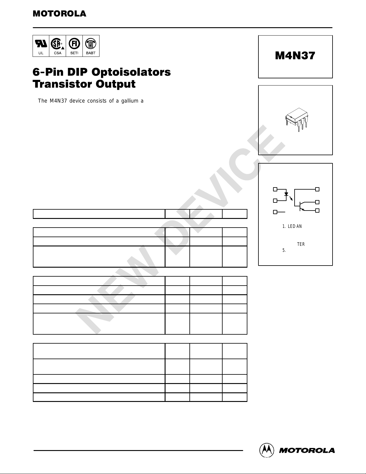
STYLE 1 PLASTIC
6
1
STANDARD THRU HOLE
SCHEMATIC
1
6
MAXIMUM RATINGS
INPUT LED
Reverse Voltage V
Forward Current — Continuous I
LED Power Dissipation @ TA = 25°C
with Negligible Power in Output Detector
Derate above 25°C
OUTPUT TRANSISTOR
Collector–Emitter Voltage V
Emitter–Base Voltage V
Collector–Base Voltage V
Collector Current — Continuous I
Detector Power Dissipation @ TA = 25°C
with Negligible Power in Input LED
Derate above 25°C
TOTAL DEVICE
Isolation Source Voltage
(Peak ac Voltage, 60 Hz, 1 sec Duration)
Total Device Power Dissipation @ TA = 25°C
Derate above 25°C
Ambient Operating Temperature Range
Storage Temperature Range
Soldering Temperature (10 sec, 1/16″ from case) T
1. Isolation surge voltage is an internal device dielectric breakdown rating.
1. For this test, Pins 1 and 2 are common, and Pins 4, 5 and 6 are common.
2. Refer to Quality and Reliability Section in Opto Data Book for information on test conditions.
(TA = 25°C unless otherwise noted)
Rating
(1)
(2)
(2)
Symbol Value Unit
6 Volts
60 mA
100
1.41
30 Volts
7 Volts
70 Volts
50 mA
150
1.76
7500 Vac(pk)
250
2.94
–55 to +100 °C
–55 to +150 °C
260 °C
mW/°C
mW/°C
mW/°C
P
CEO
EBO
CBO
P
V
ISO
P
T
T
R
F
D
C
D
D
A
stg
L
mW
mW
mW
2
3
PIN 1. LED ANODE
2. LED CATHODE
3. N.C.
4. EMITTER
5. COLLECTOR
6. BASE
5
4
Motorola Optoelectronics Device Data
Motorola, Inc. 1997
1
M4N37
(
C
,
CC
,
ELECTRICAL CHARACTERISTICS
Characteristic
INPUT LED
Forward Voltage (IF = 10 mA) TA = 25°C
Reverse Leakage Current (VR = 6 V) I
Capacitance (V = 0 V, f = 1 MHz) C
OUTPUT TRANSISTOR
Collector–Emitter Dark Current (VCE = 10 V, TA = 25°C)
Collector–Base Dark Current (VCB = 10 V) TA = 25°C
Collector–Emitter Breakdown Voltage (IC = 1 mA) V
Collector–Base Breakdown Voltage (IC = 100 µA) V
Emitter–Base Breakdown Voltage (IE = 100 µA) V
DC Current Gain (IC = 2 mA, VCE = 5 V) h
Collector–Emitter Capacitance (f = 1 MHz, VCE = 0) C
Collector–Base Capacitance (f = 1 MHz, VCB = 0) C
Emitter–Base Capacitance (f = 1 MHz, VEB = 0) C
COUPLED
Output Collector Current TA = 25°C
(IF = 10 mA, VCE = 10 V) TA = –55°C
Collector–Emitter Saturation Voltage (IC = 0.5 mA, IF = 10 mA) V
Turn–On Time
Turn–Off Time
Rise Time
Fall Time t
Isolation Voltage (f = 60 Hz, t = 1 sec) V
Isolation Current
Isolation Resistance (V = 500 V)
Isolation Capacitance (V = 0 V , f = 1 MHz)
1. Always design to the specified minimum/maximum electrical limits (where applicable).
2. Current Transfer Ratio (CTR) = IC/IF x 100%.
3. For test circuit setup and waveforms, refer to Figure 14.
4. For this test, Pins 1 and 2 are common, and Pins 4, 5 and 6 are common.
(4)
(V
= 1500 Vpk) I
I–O
(TA = 25°C unless otherwise noted)
TA = –55°C
TA = 100°C
(VCE = 30 V, TA = 100°C)
TA = 100°C
TA = 100°C
(IC = 2 mA, VCC = 10 V,
RL = 100 Ω)
(4)
(4)
(3)
(1)
Symbol Min Typ
V
R
I
CEO
I
CBO
(BR)CEO
(BR)CBO
(BR)EBO
FE
CE
CB
EB
IC (CTR)
CE(sat)
t
on
t
off
t
ISO
ISO
R
ISO
C
ISO
F 0.8
J
(2)
r
f
0.9
0.7
— — 10 µA
— 18 — pF
—
—
— 0.2
30 45 — Volts
70 100 — Volts
— 400 — —
— 7 — pF
— 19 — pF
— 9 — pF
10 (100)
4 (40)
4 (40)
— 0.14 0.3 Volts
— 7.5 10
— 5.7 10
— 3.2 —
— 4.7 —
7500 — — Vac(pk)
— 8 100 µA
10
— 0.2 2 pF
(1)
1.15
1.3
1.05
1
—
100
7 7.8 — Volts
30 (300)
—
—
11
— — Ω
Max Unit
1.5
1.7
1.4
50
500
20
—
—
—
—
Volts
nA
µA
nA
mA (%)
µs
2
Motorola Optoelectronics Device Data
1.4
1.3
1.2
1.1
TA = –55°C
TA = 25°C
1.5
NORMALIZED TO:
VCE = 10 V
IF = 10 mA
TA = 25
1.0
CTR
°
C
CE(sat) VCE
= 0.4 V
NCTR
NCTR
M4N37
(sat)
, FORWARD VOLTAGE (V)
F
V
1.0
0.9
0.8
0.7
TA = 85°C
0.5
NCTR, NORMALIZED CTR
1.0 1.0
IF, FORWARD CURRENT (mA)
10 1000.1
0
TA = 25°C
10 1000
IF, LED CURRENT (mA)
Figure 1. Forward Voltage vs. Forward Current Figure 2. Normalized Non–Saturated and
Saturated CTR, TA = 25°C vs. LED Current
1.5
NORMALIZED TO:
VCE = 10 V
IF = 10 mA
TA = 25
°
CTR
CE(sat) VCE
C
= 0.4 V
1.0
0.5
NCTR, NORMALIZED CTR
NCTR
TA = 50°C
NCTR
(sat)
1.5
NORMALIZED TO:
VCE = 10 V
IF = 10 mA
TA = 25
°
CTR
CE(sat) VCE
C
= 0.4 V
1.0
0.5
NCTR, NORMALIZED CTR
NCTR
TA = 70°C
NCTR
(sat)
0
1.0
IF, LED CURRENT (mA)
10 1000.1
Figure 3. Normalized Non–Saturated and Saturated
CTR, TA = 50°C vs. LED Current
1.5
NORMALIZED TO:
VCE = 10 V
IF = 10 mA
TA = 25
°
CTR
CE(sat) VCE
C
= 0.4 V
1.0
IF, LED CURRENT (mA)
1.0
0.5
NCTR, NORMALIZED CTR
0
0
1.0
IF, LED CURRENT (mA)
10 1000.1
Figure 4. Normalized Non–Saturated and Saturated
CTR, TA = 70°C vs. LED Current
NCTR
TA = 85°C
NCTR
(sat)
10 1000.1
Figure 5. Normalized Non–Saturated and Saturated
Motorola Optoelectronics Device Data
CTR, TA = 85°C vs. LED Current
3
 Loading...