


Mitsubishi M2V64S30DTP-8L, M2V64S30DTP-8, M2V64S30DTP-7L, M2V64S30DTP-7, M2V64S30DTP-6L Datasheet
...MITSUBISHI LSIs M2V64S20DTP-6,-6L,-7,-7L,-8,-8L |
(4-BANK x 4,194,304-WORD x |
4-BIT) |
||
SDRAM (Rev.3.2) |
M2V64S30DTP-6,-6L,-7,-7L,-8,-8L |
(4-BANK x 2,097,152-WORD x |
8-BIT) |
|
M2V64S40DTP-6,-6L,-7,-7L,-8,-8L |
(4-BANK x 1,048,576-WORD x 16-BIT) |
|||
|
||||
Feb.'00
64M Synchronous DRAM
PRELIMINARY
Some of contents are described for general products and are subject to change w ithout notice.
DESCRIPTION
M 2V64S20DTP is a 4-bank x 4,194,304-word x 4-bit,
M 2V64S30DTP is a 4-bank x 2,097,152-word x 8-bit,
M 2V64S40DTP is a 4-bank x 1,048,576-word x 16-bit,
synchronous DRAM , with LVTTL interface. All inputs and outputs are referenced to the rising edge of CLK. M 2V64S20DTP, M 2V64S30DTP and M 2V64S40DTP achieve very high speed data rate up to 133MHz for -6, and are suitable for main memory or graphic memory in computer systems.
FEATURES
|
|
|
|
|
M2V64S20/30/40DTP |
||
|
ITEM |
|
|
|
|
|
|
|
|
|
|
-6 |
-7 |
-8 |
|
|
|
|
|
|
|||
tCLK |
Clock Cycle T ime |
|
(Min.) |
7.5ns |
10ns |
10ns |
|
tRAS |
Active to Precharge Command Period |
(Min.) |
45ns |
50ns |
50ns |
||
tRCD |
Row to Column Delay |
|
(Min.) |
20ns |
20ns |
20ns |
|
tAC |
Access Time from CLK |
|
(Max.) (CL=3) |
5.4ns |
6ns |
6ns |
|
tRC |
Ref /Active Command Period |
(Min.) |
67.5ns |
70ns |
70ns |
||
|
Operation Current |
(Max.) |
|
V64S20D |
75mA |
70mA |
70mA |
Icc1 |
|
V64S30D |
75mA |
70mA |
70mA |
||
|
(Single Bank) |
|
|||||
|
|
|
V64S40D |
85mA |
80mA |
80mA |
|
|
|
|
|
||||
Icc6 |
Self Refresh Current |
|
(Max.) |
1mA |
1mA |
1mA |
|
-Single 3.3v±0.3V power supply
-Max. Clock frequency -6:133MHz<3-3-3>, -7:100MHz<2-2-2>, -8:100MHz<3-2-2>
-Fully Synchronous operation referenced to clock rising edge
-4 bank operation controlled by BA0 & BA1 (Bank Address)
-/CAS latency- 2 and 3 (programmable)
-Burst length- 1, 2, 4, 8 and full page (programmable)
-Burst typesequential and interleave (programmable)
-Byte ControlDQM L and DQMU for M2V64S40DTP
-Random column access
-Auto p recharge and All bank precharge controlled by A10
-Auto refresh and Self refresh
-4096 refresh cycles every 64ms
-LVTTL Interface
-400-mil, 54-pin Thin Small Outline Package (TSOP II) with 0.8mm lead pitch
 MITSUBISHI ELECTRIC
1
MITSUBISHI LSIs M2V64S20DTP-6,-6L,-7,-7L,-8,-8L |
(4-BANK x 4,194,304-WORD x |
4-BIT) |
|||||||||||||||||
SDRAM (Rev.3.2) |
M2V64S30DTP-6,-6L,-7,-7L,-8,-8L |
(4-BANK x 2,097,152-WORD x |
8-BIT) |
||||||||||||||||
M2V64S40DTP-6,-6L,-7,-7L,-8,-8L |
(4-BANK x 1,048,576-WORD x 16-BIT) |
||||||||||||||||||
|
Feb.'00 |
|
|
||||||||||||||||
|
|
|
|
|
|
|
|
|
|
|
64M Synchronous DRAM |
||||||||
|
|
|
|
|
|
|
|
|
|
|
|
|
|||||||
|
|
|
|
|
|
|
|
|
|
|
|
|
|
|
|
||||
|
|
PIN CONFIGURATION (TOP VIEW) |
|
|
|
|
|
|
|
|
|
|
|||||||
|
|
|
|
|
|
|
|
|
|
M2V64S20DTP |
|
|
|
|
|
|
|||
|
|
|
|
|
|
|
|
|
|
|
|
|
|
|
|
|
|||
|
|
|
|
|
|
|
|
|
|
M2V64S30DTP |
|
|
|
|
|
|
|||
|
|
|
|
|
|
|
|
|
|
|
|
|
|
|
|
|
|||
|
|
|
|
|
|
|
|
|
|
M2V64S40DTP |
|
|
|
|
|
|
|||
|
|
|
|
|
|
|
|
|
|
|
|
|
|
|
|
||||
|
|
|
|
|
|
|
|
|
PIN CONFIGURATION |
|
|
|
|
|
|
||||
|
|
|
|
|
|
|
|
|
|
(TOP VIEW) |
|
|
|
|
|
|
|||
|
|
|
|
|
|
|
|
|
|
|
|
|
|
|
|
|
|
|
|
|
Vdd |
Vdd |
|
Vdd |
|
1 |
54 |
|
|
Vss |
Vss |
Vss |
|||||||
|
|
|
|
|
|||||||||||||||
|
NC |
DQ0 |
|
DQ0 |
|
2 |
53 |
|
|
DQ15 |
DQ7 |
NC |
|||||||
|
|
|
|
|
|||||||||||||||
|
VddQ |
VddQ |
|
VddQ |
|
|
|
VssQ |
VssQ |
VssQ |
|||||||||
|
|
|
3 |
52 |
|
|
|||||||||||||
|
NC |
NC |
|
DQ1 |
|
|
|
DQ14 |
NC |
NC |
|||||||||
|
|
|
4 |
51 |
|
|
|||||||||||||
|
DQ0 |
DQ1 |
|
DQ2 |
|
|
|
DQ13 |
DQ6 |
DQ3 |
|||||||||
|
|
|
5 |
50 |
|
|
|||||||||||||
|
VssQ |
VssQ |
|
VssQ |
|
|
|
VddQ |
VddQ |
VddQ |
|||||||||
|
|
|
6 |
49 |
|
|
|||||||||||||
|
NC |
NC |
|
DQ3 |
|
|
|
DQ12 |
NC |
NC |
|||||||||
|
|
|
7 |
48 |
|
|
|||||||||||||
|
NC |
DQ2 |
|
DQ4 |
|
|
|
DQ11 |
DQ5 |
NC |
|||||||||
|
|
|
8 |
47 |
|
|
|||||||||||||
|
VddQ |
VddQ |
|
VddQ |
|
|
|
VssQ |
VssQ |
VssQ |
|||||||||
|
|
|
9 |
46 |
|
|
|||||||||||||
|
NC |
NC |
|
DQ5 |
|
|
|
DQ10 |
NC |
NC |
|||||||||
|
|
|
10 |
45 |
|
|
|||||||||||||
|
|
|
|
|
|||||||||||||||
|
DQ1 |
DQ3 |
|
DQ6 |
|
|
|
DQ9 |
DQ4 |
DQ2 |
|||||||||
|
|
|
11 |
44 |
|
|
|||||||||||||
|
VssQ |
VssQ |
|
VssQ |
|
|
|
VddQ |
VddQ |
VddQ |
|||||||||
|
|
|
12 |
43 |
|
|
|||||||||||||
|
NC |
NC |
|
DQ7 |
|
|
|
DQ8 |
NC |
NC |
|||||||||
|
|
|
13 |
42 |
|
|
|||||||||||||
|
Vdd |
Vdd |
|
Vdd |
|
14 |
41 |
|
|
Vss |
Vss |
Vss |
|||||||
|
|
|
|
|
|||||||||||||||
|
NC |
NC |
|
DQML |
|
|
|
NC |
NC |
NC |
|||||||||
|
|
|
15 |
40 |
|
|
|||||||||||||
|
/WE |
/WE |
|
/WE |
|
|
|
DQMU |
DQM |
DQM |
|||||||||
|
|
|
16 |
39 |
|
|
|||||||||||||
|
/CAS |
/CAS |
|
/CAS |
|
|
|
CLK |
CLK |
CLK |
|||||||||
|
|
|
17 |
38 |
|
|
|||||||||||||
|
/RAS |
/RAS |
|
/RAS |
|
|
|
CKE |
CKE |
CKE |
|||||||||
|
|
|
18 |
37 |
|
|
|||||||||||||
|
/CS |
/CS |
|
/CS |
|
|
|
NC |
NC |
NC |
|||||||||
|
|
|
19 |
36 |
|
|
|||||||||||||
|
BA0(A13) |
BA0(A13) |
BA0(A13) |
|
|
|
A11 |
A11 |
A11 |
||||||||||
|
|
20 |
35 |
|
|
||||||||||||||
|
BA1(A12) |
BA1(A12) |
BA1(A12) |
|
|
|
A9 |
A9 |
A9 |
||||||||||
|
|
21 |
34 |
|
|
||||||||||||||
|
A10(AP) |
A10(AP) |
|
A10(AP) |
|
|
|
A8 |
A8 |
A8 |
|||||||||
|
|
|
22 |
33 |
|
|
|||||||||||||
|
A0 |
A0 |
|
A0 |
|
|
|
A7 |
A7 |
A7 |
|||||||||
|
|
|
23 |
32 |
|
|
|||||||||||||
|
A1 |
A1 |
|
A1 |
|
|
|
A6 |
A6 |
A6 |
|||||||||
|
|
|
24 |
31 |
|
|
|||||||||||||
|
A2 |
A2 |
|
A2 |
|
|
|
A5 |
A5 |
A5 |
|||||||||
|
|
|
25 |
30 |
|
|
|||||||||||||
|
A3 |
A3 |
|
A3 |
|
|
|
A4 |
A4 |
A4 |
|||||||||
|
|
|
26 |
29 |
|
|
|||||||||||||
|
Vdd |
Vdd |
|
Vdd |
|
|
|
Vss |
Vss |
Vss |
|||||||||
|
|
|
27 |
28 |
|
|
|||||||||||||
|
|
|
|
|
|
|
|
|
|
|
|
|
|
|
|
|
|||
CLK |
: Master Clock |
DQM |
: Output Disable/ Write Mask |
|
CKE |
: Clock Enable |
A0-11 |
: Address Input |
|
/CS |
: Chip Select |
|||
BA0,1 |
: Bank Address |
|||
/RAS |
: Row Address Strobe |
|||
Vdd |
: Power Supply |
|||
/CAS |
: Column Address Strobe |
|||
VddQ |
: Power Supply for Output |
|||
/WE |
: Write Enable |
|||
Vss |
: Ground |
|||
DQ0-15 |
: Data I/O |
|||
VssQ |
: Ground for Output |
|||
|
|
 MITSUBISHI ELECTRIC
2
MITSUBISHI LSIs M2V64S20DTP-6,-6L,-7,-7L,-8,-8L |
(4-BANK x 4,194,304-WORD x |
4-BIT) |
||
SDRAM (Rev.3.2) |
M2V64S30DTP-6,-6L,-7,-7L,-8,-8L |
(4-BANK x 2,097,152-WORD x |
8-BIT) |
|
M2V64S40DTP-6,-6L,-7,-7L,-8,-8L |
(4-BANK x 1,048,576-WORD x 16-BIT) |
|||
|
||||
Feb.'00
64M Synchronous DRAM
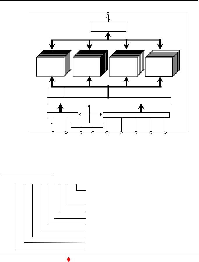
BLOCK DIAGRAM
|
|
|
|
DQ0-7 |
|
|
|
|
|
|
|
I/O Buffer |
|
|
|
||
Memory Array |
Memory Array |
|
Memory Array |
Memory Array |
||||
4096 x512 x8 |
|
4096 x512 x8 |
|
4096 x512 x8 |
4096 x512 x8 |
|||
Cell Array |
|
Cell Array |
|
Cell Array |
|
Cell Array |
||
Bank #0 |
|
Bank #1 |
|
Bank #2 |
|
Bank #3 |
||
Mode |
|
|
|
|
|
|
|
|
Register |
|
|
|
|
|
|
|
|
|
|
|
Control Circuitry |
|
|
|
||
Address Buffer |
|
|
|
Control Signal Buffer |
|
|||
|
|
Clock Buffer |
|
|
|
|
|
|
A0-11 |
BA0,1 |
CLK |
CKE |
/CS |
/RAS |
/CAS |
/WE |
DQM |
Note : This figure shows the M2V64S30DTP.
The M2V64S20DTP configration is 4096x1024x4 of cell array and DQ 0-3.
The M2V64S40DTP configration is 4096x256x16 of cell array and DQ 0-15.
Type Designation Code
M2 V 64 S 3 0 D TP -8
These rules are only applied to the Synchronous DRAM family.
Access Item |
-6 |
: 7.5ns (PC133 |
3-3-3), |
|
|
-7 |
: |
10ns (PC100 |
2-2-2), |
|
-8 |
: |
10ns (PC100 |
3-2-2) |
P ackage T ype |
T P : T S O P (II) |
|
||
P rocess Generation |
D |
: |
5th gen. |
|
Function |
R eserved for Future Use |
|||
Organization |
2 : x4, 3 : x8, 4 : x16 |
|||
Synchronous DRAM |
|
|
|
|
Density |
64 : 64Mbit |
|
||
Interface |
V : LVT T L |
|
||
Mitsubishi DRAM |
|
|
|
|
 MITSUBISHI ELECTRIC
3

MITSUBISHI LSIs |
|
M2V64S20DTP-6,-6L,-7,-7L,-8,-8L |
(4-BANK x 4,194,304-WORD x |
4-BIT) |
|||||
SDRAM (Rev.3.2) |
M2V64S30DTP-6,-6L,-7,-7L,-8,-8L |
(4-BANK x 2,097,152-WORD x |
8-BIT) |
||||||
M2V64S40DTP-6,-6L,-7,-7L,-8,-8L |
(4-BANK x 1,048,576-WORD x 16-BIT) |
||||||||
|
Feb.'00 |
|
|||||||
|
|
|
|
64M Synchronous DRAM |
|||||
|
|
|
|
|
|
||||
|
|
|
|
|
|
|
|
||
|
PIN FUNCTION |
|
|
|
|
|
|||
|
|
|
|
|
|
|
|
|
|
|
CLK |
|
|
Input |
Master Clock: |
|
|
|
|
|
|
|
All other inputs are referenced to the rising edge of CLK. |
|
|
||||
|
|
|
|
|
|
|
|||
|
|
|
|
|
|
|
|
|
|
|
|
|
|
|
Clock Enable: |
|
|
|
|
|
|
|
|
|
CKE controls internal clock. When CKE is low, internal clock for the |
|
|||
|
CKE |
|
|
Input |
following cycle is ceased. CKE is also used to select auto / |
|
|||
|
|
|
|
|
selfrefresh. After self refresh mode is started, CKE becomes |
|
|||
|
|
|
|
|
asynchronous input. Self refresh is maintained as long as CKE is low. |
|
|||
|
|
|
|
|
|
|
|
|
|
|
/CS |
|
|
Input |
Chip Select: |
|
|
|
|
|
|
|
When /CS is high, any command means No Operation. |
|
|
||||
|
|
|
|
|
|
|
|||
|
|
|
|
|
|
|
|
||
|
/RAS, /CAS, /WE |
|
|
Input |
Combination of /RAS, /CAS, /WE defines basic commands. |
|
|
||
|
|
|
|
|
|
|
|||
|
|
|
|
|
A0-11 specify the Row / Column Address in conjunction with BA0,1. |
|
|||
|
|
|
|
|
The Row Address is specified by A0-11. The Column Address is |
|
|
||
|
A0-11 |
|
|
Input |
specified by A0-9 (x4) / A0-8 (x8) / A0-7 (x16). |
|
|
||
|
|
|
A10 is also used to indicate precharge option. When A10 is high at a |
|
|||||
|
|
|
|
|
|
||||
|
|
|
|
|
read / write command, an auto precharge is performed. When A10 is |
|
|||
|
|
|
|
|
high at a precharge command, all banks are precharged. |
|
|
||
|
|
|
|
|
|
|
|
|
|
|
|
|
|
|
Bank Address: |
|
|
|
|
|
BA0,1 |
|
|
Input |
BA0,1 specifies one of four banks to which a command is applied. |
|
|||
|
|
|
|
|
BA0,1 must be set with ACT, PRE, READ, WRITE commands. |
|
|
||
|
|
|
|
|
|
|
|
||
|
DQ0-3(x4), |
|
|
|
Data In and Data out are referenced to the rising edge of CLK. |
|
|
||
|
DQ0-7(x8), |
|
Input / Output |
|
|
|
|
||
|
DQ0-15(x16) |
|
|
|
|
|
|
|
|
|
|
|
|
|
|
|
|
|
|
|
|
|
|
|
Din Mask and Output Disable: |
|
|
|
|
|
DQM(x4,x8), |
|
|
Input |
When DQM(U, L) is high in burst write, Din for the current cycle is |
|
|||
|
DQM(U, L)(x16) |
|
|
masked. When DQM(U, L) is high in burst read, Dout is disabled at |
|
||||
|
|
|
|
|
|||||
|
|
|
|
|
the next but one cycle. |
|
|
|
|
|
|
|
|
|
|
|
|||
|
Vdd, Vss |
|
Power Supply |
Power Supply for the memory array and peripheral circuitry. |
|
|
|||
|
|
|
|
|
|
|
|||
|
VddQ, VssQ |
|
Power Supply |
VddQ and VssQ are supplied to the Output Buffers only. |
|
|
|||
|
|
|
|
|
|
|
|
|
|
 MITSUBISHI ELECTRIC
4
MITSUBISHI LSIs M2V64S20DTP-6,-6L,-7,-7L,-8,-8L |
(4-BANK x 4,194,304-WORD x |
4-BIT) |
||
SDRAM (Rev.3.2) |
M2V64S30DTP-6,-6L,-7,-7L,-8,-8L |
(4-BANK x 2,097,152-WORD x |
8-BIT) |
|
M2V64S40DTP-6,-6L,-7,-7L,-8,-8L |
(4-BANK x 1,048,576-WORD x 16-BIT) |
|||
|
||||
Feb.'00
64M Synchronous DRAM
BASIC FUNCTIONS
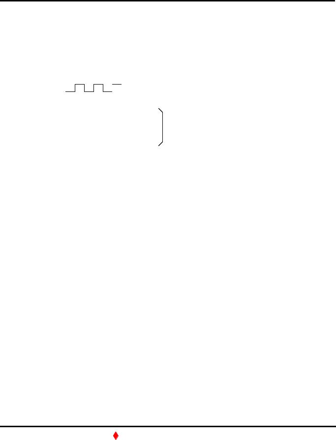
The M 2V64S20, 30 and 40DTP p rovides basic functions, bank (row) activate, burst read and write, bank (row) precharge, and auto and self refresh. Each command is defined by control signals of /RAS, /CAS and /WE at CLK rising edge. In addition to 3 signals, /CS ,CKE and A10 are used as chip select, refresh option, and precharge option, respectively. To know the detailed definition of commands, please see the command truth table.
CLK
/CS |
|
|
|
Chip Select : L=select, H=deselect |
|
/RAS |
|
|
|
Command |
|
|
|
|
|
||
/CAS |
|
|
|
Command |
def ine basic commands |
|
|
|
|||
/WE |
|
|
|
Command |
|
|
|
|
|
||
CKE |
|
|
|
Ref resh Option @ref resh command |
|
|
|
|
|||
A10 |
|
|
|
Precharge Option @precharge or read/write command |
|
|
|
|
|||
Activate (ACT) [/RAS =L, /CAS =/WE =H]
ACT command activates a row in an idle bank indicated by BA.
Read (READ) [/RAS =H, /CAS =L, /WE =H]
READ command starts burst read from the active bank indicated by BA. First output data appears after /CAS latency. When A10 =H at this command, the bank is deactivated after the burst read (autoprecharge,READA)
Write (WRITE) [/RAS =H, /CAS =/WE =L]
WRITE command starts burst write to the active bank indicated by BA. Total data length to be written is set by burst length. When A10 =H at this command, the bank is deactivated after the burst write (auto-p recharge, WRITEA).
Precharge (PRE) [/RAS =L, /CAS =H, /WE =L]
PRE command deactivates the active bank indicated by BA. This command also terminates burst read /write operation. When A10 =H at this command, all banks are deactivated (p recharge all, PREA).
Auto-Refresh (REFA) [/RAS =/CAS =L, /WE =CKE =H]
REFA command starts auto-refresh cy cle. Refresh address are generated internally. After this command, the banks are precharged automatically.
 MITSUBISHI ELECTRIC
5

MITSUBISHI LSIs |
M2V64S20DTP-6,-6L,-7,-7L,-8,-8L |
(4-BANK x 4,194,304-WORD x |
4-BIT) |
||||||||||||||
SDRAM (Rev.3.2) |
M2V64S30DTP-6,-6L,-7,-7L,-8,-8L |
(4-BANK x 2,097,152-WORD x |
8-BIT) |
||||||||||||||
M2V64S40DTP-6,-6L,-7,-7L,-8,-8L |
(4-BANK x 1,048,576-WORD x 16-BIT) |
||||||||||||||||
|
|
Feb.'00 |
|||||||||||||||
|
|
|
|
|
|
|
|
|
64M Synchronous DRAM |
||||||||
|
|
|
|
|
|
|
|
|
|
||||||||
|
|
|
|
|
|
|
|
|
|
|
|
|
|
|
|
||
|
|
COMMAND TRUTH TABLE |
|
|
|
|
|
|
|
|
|
|
|
|
|||
|
|
|
|
|
|
|
|
|
|
|
|
|
|
|
|
||
|
|
COMMAND |
|
MNEMONIC |
CKE |
CKE |
/CS |
/RAS |
/CAS |
/WE |
BA0,1 |
A11 |
A10 |
|
A0-9 |
||
|
|
|
|
|
n-1 |
n |
|
|
|
|
|
|
|
|
|
|
|
|
|
Deselect |
|
DESEL |
H |
X |
H |
X |
|
X |
X |
X |
X |
X |
|
X |
|
|
|
|
|
|
|
|
|
|
|
|
|
|
|
|
|
|
|
|
|
No Operation |
|
NOP |
H |
X |
L |
H |
|
H |
H |
X |
X |
X |
|
X |
|
|
|
|
|
|
|
|
|
|
|
|
|
|
|
|
|
||
|
|
Row Address Entry & |
ACT |
H |
X |
L |
L |
|
H |
H |
V |
V |
V |
|
V |
||
|
|
Bank Activate |
|
|
|
||||||||||||
|
|
|
|
|
|
|
|
|
|
|
|
|
|
|
|
||
|
|
Single Bank Precharge |
PRE |
H |
X |
L |
L |
|
H |
L |
V |
X |
L |
|
X |
||
|
|
|
|
|
|
|
|
|
|
|
|
|
|
|
|
||
|
|
Precharge All Banks |
PREA |
H |
X |
L |
L |
|
H |
L |
X |
X |
H |
|
X |
||
|
|
|
|
|
|
|
|
|
|
|
|
|
|
|
|
||
|
|
Column Address Entry |
WRITE |
H |
X |
L |
H |
|
L |
L |
V |
V |
L |
|
V |
||
|
|
& Write |
|
|
|
||||||||||||
|
|
|
|
|
|
|
|
|
|
|
|
|
|
|
|
||
|
|
Column Address Entry & |
WRITEA |
H |
X |
L |
H |
|
L |
L |
V |
V |
H |
|
V |
||
|
|
Write with Auto-Precharge |
|
|
|||||||||||||
|
|
|
|
|
|
|
|
|
|
|
|
|
|
|
|||
|
|
|
|
|
|
|
|
|
|
|
|
|
|
|
|
||
|
|
Column Address Entry |
READ |
H |
X |
L |
H |
|
L |
H |
V |
V |
L |
|
V |
||
|
|
& Read |
|
|
|
||||||||||||
|
|
|
|
|
|
|
|
|
|
|
|
|
|
|
|
||
|
|
|
|
|
|
|
|
|
|
|
|
|
|
|
|
||
|
|
Column Address Entry & |
READA |
H |
X |
L |
H |
|
L |
H |
V |
V |
H |
|
V |
||
|
|
Read with Auto-Precharge |
|
|
|||||||||||||
|
|
|
|
|
|
|
|
|
|
|
|
|
|
|
|||
|
|
|
|
|
|
|
|
|
|
|
|
|
|
|
|
|
|
|
|
Auto-Refresh |
|
REFA |
H |
H |
L |
L |
|
L |
H |
X |
X |
X |
|
X |
|
|
|
|
|
|
|
|
|
|
|
|
|
|
|
|
|
||
|
|
Self-Refresh Entry |
REFS |
H |
L |
L |
L |
|
L |
H |
X |
X |
X |
|
X |
||
|
|
|
|
|
|
|
|
|
|
|
|
|
|
|
|
|
|
|
|
|
|
|
L |
H |
H |
X |
|
X |
X |
X |
X |
X |
|
X |
|
|
|
Self-Refresh Exit |
REFSX |
|
|
|
|
|
|
|
|
|
|
|
|
||
|
|
L |
H |
L |
H |
|
H |
H |
X |
X |
X |
|
X |
||||
|
|
|
|
|
|
|
|||||||||||
|
|
|
|
|
|
|
|
|
|
|
|
|
|
|
|
|
|
|
|
Burst Terminate |
|
TBST |
H |
X |
L |
H |
|
H |
L |
X |
X |
X |
|
X |
|
|
|
|
|
|
|
|
|
|
|
|
|
|
|
|
|
||
|
|
Mode Register Set |
MRS |
H |
X |
L |
L |
|
L |
L |
L |
L |
L |
|
V*1 |
||
|
|
|
|
|
|
|
|
|
|
|
|
|
|
|
|||
|
|
H=High Level, L=Low Level, V=Valid, X=Don't Care, n=CLK cycle number |
|
|
|
|
|
||||||||||
|
|
NOTE: |
|
|
|
|
|
|
|
|
|
|
|
|
|
|
|
|
|
1. A7-A9 =0, A0-A6 |
=Mode Address |
|
|
|
|
|
|
|
|
|
|
|
|
||
 MITSUBISHI ELECTRIC
6

MITSUBISHI LSIs |
M2V64S20DTP-6,-6L,-7,-7L,-8,-8L |
(4-BANK x 4,194,304-WORD x |
4-BIT) |
|||||||||||
SDRAM (Rev.3.2) |
M2V64S30DTP-6,-6L,-7,-7L,-8,-8L |
(4-BANK x 2,097,152-WORD x |
8-BIT) |
|||||||||||
M2V64S40DTP-6,-6L,-7,-7L,-8,-8L |
(4-BANK x 1,048,576-WORD x 16-BIT) |
|||||||||||||
|
|
Feb.'00 |
|
|||||||||||
|
|
|
|
|
|
|
|
|
64M Synchronous DRAM |
|||||
|
|
|
|
|
|
|
|
|
|
|||||
|
|
|
|
|
|
|
|
|
|
|
|
|
|
|
|
|
FUNCTION TRUTH TABLE |
|
|
|
|
|
|
|
|||||
|
|
|
|
|
|
|
|
|
|
|
|
|
||
|
|
Current State |
/CS |
/RAS |
/CAS |
/WE |
Address |
Command |
Action |
|
|
|
||
|
|
|
|
|
|
|
|
|
|
|
|
|
||
|
|
IDLE |
H |
X |
X |
X |
X |
DESEL |
NOP |
|
|
|
||
|
|
|
|
|
|
|
|
|
|
|
|
|
||
|
|
|
L |
H |
H |
H |
X |
NOP |
NOP |
|
|
|
||
|
|
|
|
|
|
|
|
|
|
|
|
|
||
|
|
|
L |
H |
H |
L |
X |
TBST |
ILLEGAL*2 |
|
|
|
||
|
|
|
|
|
|
|
|
|
|
|
|
|
||
|
|
|
L |
H |
L |
X |
BA, CA, A10 |
READ & |
ILLEGAL*2 |
|
|
|
||
|
|
|
|
|
|
|
|
WRITE |
|
|
|
|
|
|
|
|
|
L |
L |
H |
H |
BA, RA |
ACT |
Bank Active, Latch RA |
|
|
|
||
|
|
|
|
|
|
|
|
|
|
|
|
|
|
|
|
|
|
L |
L |
H |
L |
BA, A10 |
PRE & |
NOP*4 |
|
|
|
||
|
|
|
PREA |
|
|
|
||||||||
|
|
|
|
|
|
|
|
|
|
|
|
|
||
|
|
|
L |
L |
L |
H |
X |
REFA |
Auto-Refresh*5 |
|
|
|
||
|
|
|
|
|
|
|
|
|
|
|
|
|
|
|
|
|
|
L |
L |
L |
L |
Op-Code, |
MRS |
Mode Register Set*5 |
|
|
|
||
|
|
|
Mode-Add |
|
|
|
||||||||
|
|
|
|
|
|
|
|
|
|
|
|
|
||
|
|
ROW ACTIVE |
H |
X |
X |
X |
X |
DESEL |
NOP |
|
|
|
||
|
|
|
|
|
|
|||||||||
|
|
|
|
|
|
|
|
|
|
|
|
|
||
|
|
|
L |
H |
H |
H |
X |
NOP |
NOP |
|
|
|
||
|
|
|
|
|
|
|
|
|
|
|
|
|
||
|
|
|
L |
H |
H |
L |
X |
TBST |
NOP |
|
|
|
||
|
|
|
|
|
|
|
|
|
|
|
|
|||
|
|
|
L |
H |
L |
H |
BA, CA, A10 |
READ & |
Begin Read, Latch CA, Determine |
|
||||
|
|
|
|
|
|
|
|
READA |
Auto-Precharge |
|
|
|
||
|
|
|
L |
H |
L |
L |
BA, CA, A10 |
WRITE & |
Begin Write, Latch CA, Determine |
|
|
|
||
|
|
|
WRITEA |
Auto-Precharge |
|
|
|
|||||||
|
|
|
|
|
|
|
|
|
|
|
||||
|
|
|
|
|
|
|
|
|
|
|
|
|
||
|
|
|
L |
L |
H |
H |
BA, RA |
ACT |
Bank Active / ILLEGAL*2 |
|
|
|
||
|
|
|
|
|
|
|
|
|
|
|
|
|
|
|
|
|
|
L |
L |
H |
L |
BA, A10 |
PRE & |
Precharge / Precharge All |
|
|
|
||
|
|
|
PREA |
|
|
|
||||||||
|
|
|
|
|
|
|
|
|
|
|
|
|
||
|
|
|
|
|
|
|
|
|
|
|
|
|
||
|
|
|
L |
L |
L |
H |
X |
REFA |
ILLEGAL |
|
|
|
||
|
|
|
|
|
|
|
|
|
|
|
|
|
|
|
|
|
|
L |
L |
L |
L |
Op-Code, |
MRS |
ILLEGAL |
|
|
|
||
|
|
|
Mode-Add |
|
|
|
||||||||
|
|
|
|
|
|
|
|
|
|
|
|
|
||
 MITSUBISHI ELECTRIC
7
MITSUBISHI LSIs |
M2V64S20DTP-6,-6L,-7,-7L,-8,-8L |
(4-BANK x 4,194,304-WORD x |
4-BIT) |
|||||||||||
SDRAM (Rev.3.2) |
M2V64S30DTP-6,-6L,-7,-7L,-8,-8L |
(4-BANK x 2,097,152-WORD x |
8-BIT) |
|||||||||||
M2V64S40DTP-6,-6L,-7,-7L,-8,-8L |
(4-BANK x 1,048,576-WORD x 16-BIT) |
|||||||||||||
|
|
Feb.'00 |
|
|||||||||||
|
|
|
|
|
|
|
|
|
64M Synchronous DRAM |
|||||
|
|
|
|
|
|
|
|
|
|
|||||
|
|
|
|
|
|
|
|
|
|
|
|
|
|
|
|
|
FUNCTION TRUTH TABLE (continued) |
|
|
|
|
|
|||||||
|
|
|
|
|
|
|
|
|
|
|
|
|
||
|
|
Current State |
/CS |
/RAS |
/CAS |
/WE |
Address |
Command |
Action |
|
|
|
||
|
|
|
|
|
|
|
|
|
|
|
|
|
||
|
|
READ |
H |
X |
X |
X |
X |
DESEL |
NOP (Continue Burst to END) |
|
|
|
||
|
|
|
|
|
|
|
|
|
|
|
|
|
||
|
|
|
L |
H |
H |
H |
X |
NOP |
NOP (Continue Burst to END) |
|
|
|
||
|
|
|
|
|
|
|
|
|
|
|
|
|
||
|
|
|
L |
H |
H |
L |
X |
TBST |
Terminate Burst |
|
|
|
||
|
|
|
|
|
|
|
|
|
|
|
|
|||
|
|
|
L |
H |
L |
H |
BA, CA, A10 |
READ |
Terminate Burst, Latch CA, Begin New |
|
||||
|
|
|
/READA |
Read, Determine Auto-Precharge*3 |
|
|||||||||
|
|
|
|
|
|
|
|
|
||||||
|
|
|
|
|
|
|
|
|
|
|
|
|
||
|
|
|
L |
H |
L |
L |
BA, CA, A10 |
WRITE & |
Terminate Burst, Latch CA, Begin |
|
|
|
||
|
|
|
WRITEA |
Write, Determine Auto-Precharge*3 |
|
|||||||||
|
|
|
|
|
|
|
|
|
||||||
|
|
|
|
|
|
|
|
|
|
|
|
|
||
|
|
|
L |
L |
H |
H |
BA, RA |
ACT |
Bank Active / ILLEGAL*2 |
|
|
|
||
|
|
|
|
|
|
|
|
|
|
|
|
|
|
|
|
|
|
L |
L |
H |
L |
BA, A10 |
PRE & |
Terminate Burst, Precharge |
|
|
|
||
|
|
|
PREA |
|
|
|
||||||||
|
|
|
|
|
|
|
|
|
|
|
|
|
||
|
|
|
L |
L |
L |
H |
X |
REFA |
ILLEGAL |
|
|
|
||
|
|
|
|
|
|
|
|
|
|
|
|
|
|
|
|
|
|
L |
L |
L |
L |
Op-Code, |
MRS |
ILLEGAL |
|
|
|
||
|
|
|
Mode-Add |
|
|
|
||||||||
|
|
|
|
|
|
|
|
|
|
|
|
|
||
|
|
WRITE |
H |
X |
X |
X |
X |
DESEL |
NOP (Continue Burst to END) |
|
|
|
||
|
|
|
|
|
|
|
|
|
|
|
|
|
||
|
|
|
L |
H |
H |
H |
X |
NOP |
NOP (Continue Burst to END) |
|
|
|
||
|
|
|
|
|
|
|
|
|
|
|
|
|
||
|
|
|
L |
H |
H |
L |
X |
TBST |
Terminate Burst |
|
|
|
||
|
|
|
|
|
|
|
|
|
|
|
|
|
||
|
|
|
L |
H |
L |
H |
BA, CA, A10 |
READ & |
Terminate Burst, Latch CA, Begin |
|
|
|
||
|
|
|
READA |
Read, Determine Auto-Precharge*3 |
|
|||||||||
|
|
|
|
|
|
|
|
|
||||||
|
|
|
|
|
|
|
|
|
|
|
|
|
||
|
|
|
L |
H |
L |
L |
BA, CA, A10 |
WRITE & |
Terminate Burst, Latch CA,Begin |
|
|
|
||
|
|
|
WRITEA |
Write, Determine Auto-Precharge*3 |
|
|||||||||
|
|
|
|
|
|
|
|
|
||||||
|
|
|
L |
L |
H |
H |
BA, RA |
ACT |
Bank Active / ILLEGAL*2 |
|
|
|
||
|
|
|
|
|
|
|
|
|
|
|
|
|
|
|
|
|
|
L |
L |
H |
L |
BA, A10 |
PRE & |
Terminate Burst, Precharge |
|
|
|
||
|
|
|
PREA |
|
|
|
||||||||
|
|
|
|
|
|
|
|
|
|
|
|
|
||
|
|
|
L |
L |
L |
H |
X |
REFA |
ILLEGAL |
|
|
|
||
|
|
|
|
|
|
|
|
|
|
|
|
|
|
|
|
|
|
L |
L |
L |
L |
Op-Code, |
MRS |
ILLEGAL |
|
|
|
||
|
|
|
Mode-Add |
|
|
|
||||||||
|
|
|
|
|
|
|
|
|
|
|
|
|
||
 MITSUBISHI ELECTRIC
8
MITSUBISHI LSIs |
M2V64S20DTP-6,-6L,-7,-7L,-8,-8L |
(4-BANK x 4,194,304-WORD x |
4-BIT) |
|||||||||||
SDRAM (Rev.3.2) |
M2V64S30DTP-6,-6L,-7,-7L,-8,-8L |
(4-BANK x 2,097,152-WORD x |
8-BIT) |
|||||||||||
M2V64S40DTP-6,-6L,-7,-7L,-8,-8L |
(4-BANK x 1,048,576-WORD x 16-BIT) |
|||||||||||||
|
|
Feb.'00 |
|
|||||||||||
|
|
|
|
|
|
|
|
|
64M Synchronous DRAM |
|||||
|
|
|
|
|
|
|
|
|
|
|||||
|
|
|
|
|
|
|
|
|
|
|
|
|
|
|
|
|
FUNCTION TRUTH TABLE (continued) |
|
|
|
|
|
|||||||
|
|
|
|
|
|
|
|
|
|
|
|
|
||
|
|
Current State |
/CS |
/RAS |
/CAS |
/WE |
Address |
Command |
Action |
|
|
|
||
|
|
|
|
|
|
|
|
|
|
|
|
|
||
|
|
READ with |
H |
X |
X |
X |
X |
DESEL |
NOP (Continue Burst to END) |
|
|
|
||
|
|
AUTO |
|
|
|
|
|
|
|
|
|
|
|
|
|
|
L |
H |
H |
H |
X |
NOP |
NOP (Continue Burst to END) |
|
|
|
|||
|
|
PRECHARGE |
|
|
|
|||||||||
|
|
|
|
|
|
|
|
|
|
|
|
|
||
|
|
|
L |
H |
H |
L |
X |
TBST |
ILLEGAL |
|
|
|
||
|
|
|
|
|
|
|
|
|
|
|
|
|
|
|
|
|
|
L |
H |
L |
H |
BA, CA, A10 |
READ & |
ILLEGAL |
|
|
|
||
|
|
|
READA |
|
|
|
||||||||
|
|
|
|
|
|
|
|
|
|
|
|
|
||
|
|
|
|
|
|
|
|
|
|
|
|
|
|
|
|
|
|
L |
H |
L |
L |
BA, CA, A10 |
WRITE & |
ILLEGAL |
|
|
|
||
|
|
|
WRITEA |
|
|
|
||||||||
|
|
|
|
|
|
|
|
|
|
|
|
|
||
|
|
|
L |
L |
H |
H |
BA, RA |
ACT |
Bank Active / ILLEGAL*2 |
|
|
|
||
|
|
|
|
|
|
|
|
|
|
|
|
|
|
|
|
|
|
L |
L |
H |
L |
BA, A10 |
PRE & |
ILLEGAL*2 |
|
|
|
||
|
|
|
PREA |
|
|
|
||||||||
|
|
|
|
|
|
|
|
|
|
|
|
|
||
|
|
|
|
|
|
|
|
|
|
|
|
|
||
|
|
|
L |
L |
L |
H |
X |
REFA |
ILLEGAL |
|
|
|
||
|
|
|
|
|
|
|
|
|
|
|
|
|
|
|
|
|
|
L |
L |
L |
L |
Op-Code, |
MRS |
ILLEGAL |
|
|
|
||
|
|
|
Mode-Add |
|
|
|
||||||||
|
|
|
|
|
|
|
|
|
|
|
|
|
||
|
|
WRITE with |
H |
X |
X |
X |
X |
DESEL |
NOP (Continue Burst to END) |
|
|
|
||
|
|
AUTO |
|
|
|
|
|
|
|
|
|
|
|
|
|
|
|
|
|
|
|
|
|
|
|
|
|
||
|
|
PRECHARGE |
L |
H |
H |
H |
X |
NOP |
NOP (Continue Burst to END) |
|
|
|
||
|
|
|
|
|
|
|
|
|
|
|
|
|
||
|
|
|
L |
H |
H |
L |
X |
TBST |
ILLEGAL |
|
|
|
||
|
|
|
|
|
|
|
|
|
|
|
|
|
|
|
|
|
|
L |
H |
L |
H |
BA, CA, A10 |
READ & |
ILLEGAL |
|
|
|
||
|
|
|
READA |
|
|
|
||||||||
|
|
|
|
|
|
|
|
|
|
|
|
|
||
|
|
|
L |
H |
L |
L |
BA, CA, A10 |
WRITE & |
ILLEGAL |
|
|
|
||
|
|
|
WRITEA |
|
|
|
||||||||
|
|
|
|
|
|
|
|
|
|
|
|
|
||
|
|
|
L |
L |
H |
H |
BA, RA |
ACT |
Bank Active / ILLEGAL*2 |
|
|
|
||
|
|
|
|
|
|
|
|
|
|
|
|
|
|
|
|
|
|
L |
L |
H |
L |
BA, A10 |
PRE & |
ILLEGAL*2 |
|
|
|
||
|
|
|
PREA |
|
|
|
||||||||
|
|
|
|
|
|
|
|
|
|
|
|
|
||
|
|
|
|
|
|
|
|
|
|
|
|
|
||
|
|
|
L |
L |
L |
H |
X |
REFA |
ILLEGAL |
|
|
|
||
|
|
|
|
|
|
|
|
|
|
|
|
|
|
|
|
|
|
L |
L |
L |
L |
Op-Code, |
MRS |
ILLEGAL |
|
|
|
||
|
|
|
Mode-Add |
|
|
|
||||||||
|
|
|
|
|
|
|
|
|
|
|
|
|
||
 MITSUBISHI ELECTRIC
9

MITSUBISHI LSIs |
M2V64S20DTP-6,-6L,-7,-7L,-8,-8L |
(4-BANK x 4,194,304-WORD x |
4-BIT) |
||||||||||||
SDRAM (Rev.3.2) |
M2V64S30DTP-6,-6L,-7,-7L,-8,-8L |
(4-BANK x 2,097,152-WORD x |
8-BIT) |
||||||||||||
M2V64S40DTP-6,-6L,-7,-7L,-8,-8L |
(4-BANK x 1,048,576-WORD x 16-BIT) |
||||||||||||||
|
Feb.'00 |
|
|||||||||||||
|
|
|
|
|
|
|
|
64M Synchronous DRAM |
|||||||
|
|
|
|
|
|
|
|
|
|
|
|||||
|
|
|
|
|
|
|
|
|
|
|
|
|
|
|
|
|
|
FUNCTION TRUTH TABLE (continued) |
|
|
|
|
|
||||||||
|
|
Current State |
/CS |
/RAS |
/CAS |
/WE |
Address |
Command |
Action |
|
|
|
|||
|
|
|
|
|
|
|
|
|
|
|
|
|
|
||
|
|
PRE - |
H |
X |
X |
X |
X |
DESEL |
NOP (Idle after tRP) |
|
|
|
|||
|
|
CHARGING |
|
|
|
|
|
|
|
|
|
|
|
|
|
|
|
|
L |
H |
H |
H |
X |
NOP |
NOP (Idle after tRP) |
|
|
|
|||
|
|
|
|
|
|
|
|||||||||
|
|
|
|
|
|
|
|
|
|
|
|
|
|
||
|
|
|
|
L |
H |
H |
L |
X |
TBST |
ILLEGAL*2 |
|
|
|
||
|
|
|
|
|
|
|
|
|
|
|
|
|
|
|
|
|
|
|
|
L |
H |
L |
X |
BA, CA, A10 |
READ & |
ILLEGAL*2 |
|
|
|
||
|
|
|
|
WRITE |
|
|
|
||||||||
|
|
|
|
|
|
|
|
|
|
|
|
|
|
||
|
|
|
|
|
|
|
|
|
|
|
|
|
|
||
|
|
|
|
L |
L |
H |
H |
BA, RA |
ACT |
ILLEGAL*2 |
|
|
|
||
|
|
|
|
|
|
|
|
|
|
|
|
|
|
|
|
|
|
|
|
L |
L |
H |
L |
BA, A10 |
PRE & |
NOP*4 (Idle after tRP) |
|
|
|
||
|
|
|
|
PREA |
|
|
|
||||||||
|
|
|
|
|
|
|
|
|
|
|
|
|
|
||
|
|
|
|
L |
L |
L |
H |
X |
REFA |
ILLEGAL |
|
|
|
||
|
|
|
|
|
|
|
|
|
|
|
|
|
|
|
|
|
|
|
|
L |
L |
L |
L |
Op-Code, |
MRS |
ILLEGAL |
|
|
|
||
|
|
|
|
Mode-Add |
|
|
|
||||||||
|
|
|
|
|
|
|
|
|
|
|
|
|
|
||
|
|
ROW |
H |
X |
X |
X |
X |
DESEL |
NOP (Row Active after tRCD) |
|
|
|
|||
|
|
ACTIVATING |
|
|
|
|
|
|
|
|
|
|
|
||
|
L |
H |
H |
H |
X |
NOP |
NOP (Row Active after tRCD) |
|
|
|
|||||
|
|
|
|
|
|
|
|||||||||
|
|
|
|
|
|
|
|
|
|
|
|
|
|
||
|
|
|
|
L |
H |
H |
L |
X |
TBST |
ILLEGAL*2 |
|
|
|
||
|
|
|
|
|
|
|
|
|
|
|
|
|
|
||
|
|
|
|
L |
H |
L |
X |
BA, CA, A10 |
READ & |
ILLEGAL*2 |
|
|
|
||
|
|
|
|
|
|
|
|
|
WRITE |
|
|
|
|
|
|
|
|
|
|
L |
L |
H |
H |
BA, RA |
ACT |
ILLEGAL*2 |
|
|
|
||
|
|
|
|
|
|
|
|
|
|
|
|
|
|
|
|
|
|
|
|
L |
L |
H |
L |
BA, A10 |
PRE & |
ILLEGAL*2 |
|
|
|
||
|
|
|
|
PREA |
|
|
|
||||||||
|
|
|
|
|
|
|
|
|
|
|
|
|
|
||
|
|
|
|
L |
L |
L |
H |
X |
REFA |
ILLEGAL |
|
|
|
||
|
|
|
|
|
|
|
|
|
|
|
|
|
|
|
|
|
|
|
|
L |
L |
L |
L |
Op-Code, |
MRS |
ILLEGAL |
|
|
|
||
|
|
|
|
Mode-Add |
|
|
|
||||||||
|
|
|
|
|
|
|
|
|
|
|
|
|
|
||
|
|
|
|
|
|
|
|
|
|
|
|
|
|
|
|
 MITSUBISHI ELECTRIC
10
MITSUBISHI LSIs |
M2V64S20DTP-6,-6L,-7,-7L,-8,-8L |
(4-BANK x 4,194,304-WORD x |
4-BIT) |
||||||||||||
SDRAM (Rev.3.2) |
M2V64S30DTP-6,-6L,-7,-7L,-8,-8L |
(4-BANK x 2,097,152-WORD x |
8-BIT) |
||||||||||||
M2V64S40DTP-6,-6L,-7,-7L,-8,-8L |
(4-BANK x 1,048,576-WORD x 16-BIT) |
||||||||||||||
|
Feb.'00 |
|
|||||||||||||
|
|
|
|
|
|
|
|
64M Synchronous DRAM |
|||||||
|
|
|
|
|
|
|
|
|
|
|
|||||
|
|
|
|
|
|
|
|
|
|
|
|
|
|
|
|
|
|
FUNCTION TRUTH TABLE (continued) |
|
|
|
|
|
||||||||
|
|
Current State |
/CS |
/RAS |
/CAS |
/WE |
Address |
Command |
Action |
|
|
|
|||
|
|
|
|
|
|
|
|
|
|
|
|
|
|
||
|
|
WRITE |
H |
X |
X |
X |
X |
DESEL |
NOP |
|
|
|
|||
|
|
RECOVERING |
|
|
|
|
|
|
|
|
|
|
|
|
|
|
|
|
L |
H |
H |
H |
X |
NOP |
NOP |
|
|
|
|||
|
|
|
|
|
|
|
|||||||||
|
|
|
|
|
|
|
|
|
|
|
|
|
|
||
|
|
|
|
L |
H |
H |
L |
X |
TBST |
ILLEGAL*2 |
|
|
|
||
|
|
|
|
|
|
|
|
|
|
|
|
|
|
|
|
|
|
|
|
L |
H |
L |
X |
BA, CA, A10 |
READ & |
ILLEGAL*2 |
|
|
|
||
|
|
|
|
WRITE |
|
|
|
||||||||
|
|
|
|
|
|
|
|
|
|
|
|
|
|
||
|
|
|
|
|
|
|
|
|
|
|
|
|
|
||
|
|
|
|
L |
L |
H |
H |
BA, RA |
ACT |
ILLEGAL*2 |
|
|
|
||
|
|
|
|
|
|
|
|
|
|
|
|
|
|
|
|
|
|
|
|
L |
L |
H |
L |
BA, A10 |
PRE & |
ILLEGAL*2 |
|
|
|
||
|
|
|
|
PREA |
|
|
|
||||||||
|
|
|
|
|
|
|
|
|
|
|
|
|
|
||
|
|
|
|
|
|
|
|
|
|
|
|
|
|
||
|
|
|
|
L |
L |
L |
H |
X |
REFA |
ILLEGAL |
|
|
|
||
|
|
|
|
|
|
|
|
|
|
|
|
|
|
|
|
|
|
|
|
L |
L |
L |
L |
Op-Code, |
MRS |
ILLEGAL |
|
|
|
||
|
|
|
|
Mode-Add |
|
|
|
||||||||
|
|
|
|
|
|
|
|
|
|
|
|
|
|
||
|
|
REFRESHING |
H |
X |
X |
X |
X |
DESEL |
NOP (Idle after tRC) |
|
|
|
|||
|
|
|
|
|
|
|
|
|
|
|
|
|
|
||
|
|
|
|
L |
H |
H |
H |
X |
NOP |
NOP (Idle after tRC) |
|
|
|
||
|
|
|
|
|
|
|
|
|
|
|
|
|
|
||
|
|
|
|
L |
H |
H |
L |
X |
TBST |
ILLEGAL |
|
|
|
||
|
|
|
|
|
|
|
|
|
|
|
|
|
|
|
|
|
|
|
|
L |
H |
L |
X |
BA, CA, A10 |
READ & |
ILLEGAL |
|
|
|
||
|
|
|
|
WRITE |
|
|
|
||||||||
|
|
|
|
|
|
|
|
|
|
|
|
|
|
||
|
|
|
|
|
|
|
|
|
|
|
|
|
|
||
|
|
|
|
L |
L |
H |
H |
BA, RA |
ACT |
ILLEGAL |
|
|
|
||
|
|
|
|
|
|
|
|
|
|
|
|
|
|
|
|
|
|
|
|
L |
L |
H |
L |
BA, A10 |
PRE & |
ILLEGAL |
|
|
|
||
|
|
|
|
PREA |
|
|
|
||||||||
|
|
|
|
|
|
|
|
|
|
|
|
|
|
||
|
|
|
|
|
|
|
|
|
|
|
|
|
|
||
|
|
|
|
L |
L |
L |
H |
X |
REFA |
ILLEGAL |
|
|
|
||
|
|
|
|
|
|
|
|
|
|
|
|
|
|
|
|
|
|
|
|
L |
L |
L |
L |
Op-Code, |
MRS |
ILLEGAL |
|
|
|
||
|
|
|
|
Mode-Add |
|
|
|
||||||||
|
|
|
|
|
|
|
|
|
|
|
|
|
|
||
|
|
|
|
|
|
|
|
|
|
|
|
|
|
|
|
 MITSUBISHI ELECTRIC
11

MITSUBISHI LSIs |
M2V64S20DTP-6,-6L,-7,-7L,-8,-8L |
(4-BANK x 4,194,304-WORD x |
4-BIT) |
|||||||||||
SDRAM (Rev.3.2) |
M2V64S30DTP-6,-6L,-7,-7L,-8,-8L |
(4-BANK x 2,097,152-WORD x |
8-BIT) |
|||||||||||
M2V64S40DTP-6,-6L,-7,-7L,-8,-8L |
(4-BANK x 1,048,576-WORD x 16-BIT) |
|||||||||||||
|
|
Feb.'00 |
|
|||||||||||
|
|
|
|
|
|
|
|
|
64M Synchronous DRAM |
|||||
|
|
|
|
|
|
|
|
|
|
|||||
|
|
|
|
|
|
|
|
|
|
|
|
|
|
|
|
|
FUNCTION TRUTH TABLE (continued) |
|
|
|
|
|
|||||||
|
|
|
|
|
|
|
|
|
|
|
|
|
||
|
|
Current State |
/CS |
/RAS |
/CAS |
/WE |
Address |
Command |
Action |
|
|
|
||
|
|
|
|
|
|
|
|
|
|
|
|
|
||
|
|
MODE |
H |
X |
X |
X |
X |
DESEL |
NOP (Idle after tRSC) |
|
|
|
||
|
|
REGISTER |
|
|
|
|
|
|
|
|
|
|
|
|
|
|
L |
H |
H |
H |
X |
NOP |
NOP (Idle after tRSC) |
|
|
|
|||
|
|
SETTING |
|
|
|
|||||||||
|
|
|
|
|
|
|
|
|
|
|
|
|
||
|
|
|
L |
H |
H |
L |
X |
TBST |
ILLEGAL |
|
|
|
||
|
|
|
|
|
|
|
|
|
|
|
|
|
|
|
|
|
|
L |
H |
L |
X |
BA, CA, A10 |
READ & |
ILLEGAL |
|
|
|
||
|
|
|
WRITE |
|
|
|
||||||||
|
|
|
|
|
|
|
|
|
|
|
|
|
||
|
|
|
L |
L |
H |
H |
BA, RA |
ACT |
ILLEGAL |
|
|
|
||
|
|
|
|
|
|
|
|
|
|
|
|
|
|
|
|
|
|
L |
L |
H |
L |
BA, A10 |
PRE & |
ILLEGAL |
|
|
|
||
|
|
|
PREA |
|
|
|
||||||||
|
|
|
|
|
|
|
|
|
|
|
|
|
||
|
|
|
L |
L |
L |
H |
X |
REFA |
ILLEGAL |
|
|
|
||
|
|
|
|
|
|
|
|
|
|
|
|
|
|
|
|
|
|
L |
L |
L |
L |
Op-Code, |
MRS |
ILLEGAL |
|
|
|
||
|
|
|
Mode-Add |
|
|
|
||||||||
|
|
|
|
|
|
|
|
|
|
|
|
|
||
|
|
ABBREVIATIONS: |
|
|
|
|
|
|
|
|
|
|
||
|
|
H=High Level, L=Low Level, X=Don't Care |
|
|
|
|
|
|
||||||
|
|
BA=Bank Address, RA=Row Address, CA=Column Address, NOP=No OPeration |
|
|
|
|||||||||
NOTES:
1.All entries assume that CKE was High during the preceding clock cycle and the current clock cycle.
2.ILLEGAL to bank in specified state; function may be legal in the bank indicated by BA, depending on the state of that bank.
3.Must satisfy bus contention, bus turn around, write recovery requirements.
4.NOP to bank precharging or in idle state. May precharge bank indicated by BA.
5.ILLEGAL if any bank is not idle.
ILLEGAL = Device operation and/or data-integrity are not guaranteed.
 MITSUBISHI ELECTRIC
12
MITSUBISHI LSIs |
M2V64S20DTP-6,-6L,-7,-7L,-8,-8L |
(4-BANK x 4,194,304-WORD x |
4-BIT) |
|||||||||||||
SDRAM (Rev.3.2) |
M2V64S30DTP-6,-6L,-7,-7L,-8,-8L |
(4-BANK x 2,097,152-WORD x |
8-BIT) |
|||||||||||||
M2V64S40DTP-6,-6L,-7,-7L,-8,-8L |
(4-BANK x 1,048,576-WORD x 16-BIT) |
|||||||||||||||
|
Feb.'00 |
|
||||||||||||||
|
|
|
|
|
|
|
|
|
|
|
64M Synchronous DRAM |
|||||
|
|
|
|
|
|
|
|
|
|
|
|
|
||||
|
|
|
|
|
|
|
|
|
|
|
|
|
|
|
||
|
|
FUNCTION TRUTH TABLE for CKE |
|
|
|
|
|
|
||||||||
|
|
|
|
|
|
|
|
|
|
|
|
|
|
|
|
|
|
|
Current State |
CKE |
|
CKE |
/CS |
/RAS |
/CAS |
|
/WE |
Add |
Action |
|
|
|
|
|
|
n-1 |
|
n |
|
|
|
|
||||||||
|
|
|
|
|
|
|
|
|
|
|
|
|
|
|||
|
|
SELF- |
H |
|
X |
X |
X |
X |
|
X |
X |
INVALID |
|
|
||
|
|
|
|
|
|
|
|
|
|
|
|
|
|
|
||
|
|
REFRESH*1 |
L |
|
H |
H |
X |
X |
|
X |
X |
Exit Self-Refresh (Idle after tRC) |
|
|
||
|
|
|
L |
|
H |
L |
H |
H |
|
H |
X |
Exit Self-Refresh (Idle after tRC) |
|
|
||
|
|
|
L |
|
H |
L |
H |
H |
|
L |
X |
ILLEGAL |
|
|
||
|
|
|
L |
|
H |
L |
H |
L |
|
X |
X |
ILLEGAL |
|
|
||
|
|
|
L |
|
H |
L |
L |
X |
|
X |
X |
ILLEGAL |
|
|
||
|
|
|
L |
|
L |
X |
X |
X |
|
X |
X |
NOP (Maintain Self-Refresh) |
|
|
||
|
|
|
|
|
|
|
|
|
|
|
|
|
|
|
||
|
|
POWER |
H |
|
X |
X |
X |
X |
|
X |
X |
INVALID |
|
|
||
|
|
DOWN |
|
|
|
|
|
|
|
|
|
|
|
|
|
|
|
|
L |
|
H |
X |
X |
X |
|
X |
X |
Exit Power Down to Idle |
|
|
|||
|
|
|
|
|
|
|
||||||||||
|
|
|
L |
|
L |
X |
X |
X |
|
X |
X |
NOP (Maintain Power Down) |
|
|
||
|
|
|
|
|
|
|
|
|
|
|
|
|
|
|
||
|
|
ALL BANKS |
H |
|
H |
X |
X |
X |
|
X |
X |
Refer to Function Truth Table |
|
|
||
|
|
IDLE*2 |
|
|
|
|
|
|
|
|
|
|
|
|
|
|
|
|
H |
|
L |
L |
L |
L |
|
H |
X |
Enter Self-Refresh |
|
|
|||
|
|
|
|
|
|
|
||||||||||
|
|
|
H |
|
L |
H |
X |
X |
|
X |
X |
Enter Power Down |
|
|
||
|
|
|
H |
|
L |
L |
H |
H |
|
H |
X |
Enter Power Down |
|
|
||
|
|
|
|
|
|
|
|
|
|
|
|
|
|
|
||
|
|
|
H |
|
L |
L |
H |
H |
|
L |
X |
ILLEGAL |
|
|
||
|
|
|
H |
|
L |
L |
H |
L |
|
X |
X |
ILLEGAL |
|
|
||
|
|
|
|
|
|
|
|
|
|
|
|
|
|
|
||
|
|
|
H |
|
L |
L |
L |
X |
|
X |
X |
ILLEGAL |
|
|
||
|
|
|
L |
|
X |
X |
X |
X |
|
X |
X |
Refer to Current State =Power Down |
|
|
||
|
|
|
|
|
|
|
|
|
|
|
|
|
|
|
||
|
|
ANY STATE |
H |
|
H |
X |
X |
X |
|
X |
X |
Refer to Function Truth Table |
|
|
||
|
|
other than |
|
|
|
|
|
|
|
|
|
|
|
|
|
|
|
|
H |
|
L |
X |
X |
X |
|
X |
X |
Begin CLK Suspend at Next Cycle*3 |
|
|
|||
|
|
listed above |
|
|
|
|
||||||||||
|
|
L |
|
H |
X |
X |
X |
|
X |
X |
Exit CLK Suspend at Next Cycle*3 |
|
|
|||
|
|
|
|
|
|
|
||||||||||
|
|
|
L |
|
L |
X |
X |
X |
|
X |
X |
Maintain CLK Suspend |
|
|
||
|
|
|
|
|
|
|
|
|
|
|
|
|
|
|
|
|
|
|
ABBREVIATIONS: |
|
|
|
|
|
|
|
|
|
|
|
|
||
H=High Level, L=Low Level, X=Don't Care
NOTES:
1.CKE Low to High transition will re-enable CLK and other inputs asynchronously. A minimum setup time must be satisfied before any command other than EXIT.
2.Power-Down and Self-Refresh can be entered only from the All Banks Idle State.
3.Must be legal command.
 MITSUBISHI ELECTRIC
13

MITSUBISHI LSIs M2V64S20DTP-6,-6L,-7,-7L,-8,-8L |
(4-BANK x 4,194,304-WORD x |
4-BIT) |
||
SDRAM (Rev.3.2) |
M2V64S30DTP-6,-6L,-7,-7L,-8,-8L |
(4-BANK x 2,097,152-WORD x |
8-BIT) |
|
M2V64S40DTP-6,-6L,-7,-7L,-8,-8L |
(4-BANK x 1,048,576-WORD x 16-BIT) |
|||
|
||||
Feb.'00
64M Synchronous DRAM
SIMPLIFIED STATE DIAGRAM |
|
|
|
|
||||
|
|
|
|
|
|
SELF |
|
|
|
|
|
|
|
|
REFRESH |
|
|
|
|
|
|
REFS |
|
|
|
|
|
|
|
|
|
REFSX |
|
||
|
MODE |
MRS |
REFA |
AUTO |
|
|||
|
|
|
||||||
|
REGISTER |
|
|
|
||||
|
|
IDLE |
|
REFRESH |
|
|||
|
SET |
|
|
|
|
|
||
|
|
|
|
|
|
|
||
|
|
|
|
|
CKEL |
|
||
|
CLK |
|
|
CKEH |
|
|
|
|
|
SUSPEND |
|
|
|
|
|
|
|
|
|
|
ACT |
|
POWER |
|
||
|
|
|
CKEL |
|
|
DOWN |
|
|
|
|
|
|
|
|
|
||
|
|
CKEH |
|
|
|
|
|
|
|
|
|
ROW |
|
|
|
||
|
TERM |
ACTIVE |
TERM |
|
||||
|
|
|
|
|||||
|
|
WRITE |
|
READ |
|
|||
|
CKEL |
|
WRITEA |
READA |
|
CKEL |
|
|
WRITE |
|
|
READ |
|
READ |
|||
WRITE |
|
|
READ |
|||||
SUSPEND |
WRITE |
|
|
SUSPEND |
||||
CKEH |
|
|
|
CKEH |
||||
|
|
|
|
|
|
|||
|
WRITEA |
|
|
|
|
READA |
|
|
|
|
WRITEA |
READA |
|
|
|
||
WRITEA |
CKEL |
|
|
|
|
CKEL |
READA |
|
WRITEA |
PRE |
READA |
||||||
SUSPEND |
SUSPEND |
|||||||
CKEH |
|
|
|
|
CKEH |
|||
|
|
PRE |
PRE |
|
|
|||
|
|
|
|
|
|
|||
POWER |
|
|
|
|
|
|
|
|
APPLIED |
POWER |
PRE |
PRE |
|
|
|
||
|
ON |
CHARGE |
|
|
|
|||
|
|
|
|
|
||||
|
|
|
|
|
|
|
Automatic Sequence |
|
|
|
|
|
|
|
|
Command Sequence |
|
 MITSUBISHI ELECTRIC
14
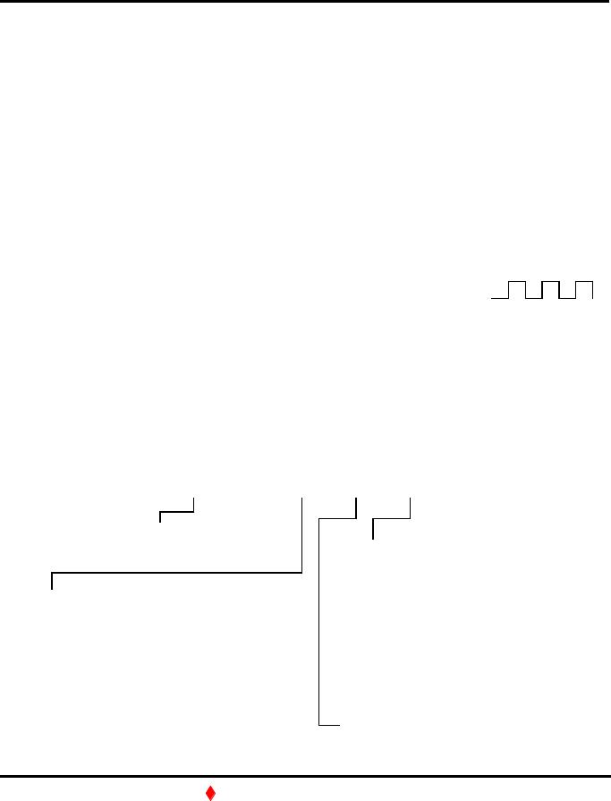
MITSUBISHI LSIs M2V64S20DTP-6,-6L,-7,-7L,-8,-8L |
(4-BANK x 4,194,304-WORD x |
4-BIT) |
||
SDRAM (Rev.3.2) |
M2V64S30DTP-6,-6L,-7,-7L,-8,-8L |
(4-BANK x 2,097,152-WORD x |
8-BIT) |
|
M2V64S40DTP-6,-6L,-7,-7L,-8,-8L |
(4-BANK x 1,048,576-WORD x 16-BIT) |
|||
|
||||
Feb.'00
64M Synchronous DRAM
POWER ON SEQUENCE
Before starting normal op eration, the following power on sequence is necessary to prevent a
SDRAM from damaged or malfunctioning.
1.Apply power and start clock. Attempt to maintain CKE high, DQM high and NOP condition at the inputs.
2.M aintain stable power, stable clock, and NOP input conditions for a minimum of 200µs.
3.Issue precharge commands for all banks. (PRE or PREA)
4.After all banks become idle state (after tRP), issue 8 or more auto-refresh commands.
5.Issue a mode register set command to initialize the mode register.
MODE REGISTER
Burst Length, Burst Type, /CAS Latency and Write M ode can be |
|
|
|
CLK |
|
|
||||||||||||||||||||||
|
|
|
/CS |
|
|
|
||||||||||||||||||||||
programmed by setting the mode register (MRS). The mode register |
|
|
|
|
|
|
||||||||||||||||||||||
|
|
|
|
|
|
|
|
|
||||||||||||||||||||
stores these data until the next MRS command, which may be issued |
/RAS |
|
|
|
||||||||||||||||||||||||
|
|
|
||||||||||||||||||||||||||
when both banks are in idle state. After tRSC from a MRS command, the |
|
|
|
|
|
|||||||||||||||||||||||
/CAS |
|
|
|
|||||||||||||||||||||||||
|
|
|
||||||||||||||||||||||||||
SDRAM is ready for new command. |
|
|
|
|
|
|
|
|
|
|
|
|
|
|
|
|
|
|||||||||||
|
|
|
|
|
|
|
|
|
|
|
|
/WE |
|
|
|
|||||||||||||
|
|
|
|
|
|
|
|
|
|
|
|
|
|
|
|
|
|
|
|
|
|
|
|
|
|
|
||
|
|
|
|
|
|
|
|
|
|
|
|
|
|
|
|
|
|
|
|
|
BA0,1 A11-A0 |
|
V |
|
||||
|
|
|
|
|
|
|
|
|
|
|
|
|
|
|
|
|
|
|
|
|
|
|
|
|
|
|
|
|
|
|
BA0 |
BA1 |
A11 |
A10 |
A9 |
|
A8 |
A7 |
A6 |
A5 |
A4 |
A3 |
A2 |
|
A1 |
A0 |
|
|
|
|
|
|
|||||
|
|
|
|
|
|
|
|
|
|
|
|
|
|
|
|
|
|
|
|
|
|
|
|
|
|
|
|
|
|
|
|
|
|
|
|
|
|
|
|
|
|
|
|
|
|
|
|
|
|
|
|
||||||
|
|
0 |
|
0 |
0 |
0 |
WM |
|
0 |
0 |
|
LTMODE |
BT |
|
BL |
|
|
|
|
|
|
|||||||
|
|
|
|
|
|
|
|
|
|
|
|
|
|
|
|
|
|
|
|
|
|
|
|
|
|
|
|
|
|
|
|
|
|
|
|
|
|
|
|
|
|
|
|
|
|
|
|
|
|
|
|
||||||
|
|
|
|
|
|
Write |
0 |
|
Burst Write |
|
|
|
|
|
|
|
|
|
|
|
|
|
||||||
|
|
|
|
|
|
Mode |
1 |
|
Single Write |
|
|
|
|
|
|
|
BL |
|
|
BT=0 |
BT=1 |
|||||||
|
|
|
|
|
|
|
|
|
|
|
|
|
|
|
|
|
|
|
|
|
0 0 0 |
|
|
1 |
1 |
|||
|
|
|
|
|
|
|
|
|
|
|
|
|
|
|
|
|
|
|
|
|
0 0 1 |
|
|
2 |
2 |
|||
|
|
|
|
CL |
|
|
/CAS LATENCY |
|
|
|
|
|
BURST |
|
0 1 0 |
|
|
4 |
4 |
|||||||||
|
|
|
0 0 0 |
|
|
|
R |
|
|
|
|
|
|
|
|
0 1 1 |
|
|
8 |
8 |
||||||||
|
|
|
|
|
|
|
|
|
|
|
|
LENGTH |
|
|
||||||||||||||
|
|
|
0 0 1 |
|
|
|
R |
|
|
|
|
|
|
|
|
1 0 0 |
|
|
R |
R |
||||||||
|
|
|
|
|
|
|
|
|
|
|
|
|
|
|
|
|
|
|||||||||||
|
LATENCY |
0 1 0 |
|
|
|
2 |
|
|
|
|
|
|
|
|
|
|
|
|
1 0 1 |
|
|
R |
R |
|||||
|
0 1 1 |
|
|
|
3 |
|
|
|
|
|
|
|
|
|
|
|
|
1 1 0 |
|
|
R |
R |
||||||
|
MODE |
|
|
|
|
|
|
|
|
|
|
|
|
|
|
|
|
|
||||||||||
|
1 0 0 |
|
|
|
R |
|
|
|
|
|
|
|
|
|
|
|
1 1 1 |
|
|
Full Page |
R |
|||||||
|
|
|
|
|
|
|
|
|
|
|
|
|
|
|
|
|
|
|||||||||||
|
|
1 0 1 |
|
|
|
R |
|
|
|
|
|
|
|
|
|
|
|
|
|
|
|
|
|
|
|
|||
|
|
1 1 0 |
|
|
|
R |
|
|
|
|
|
|
|
BURST |
|
0 |
|
|
SEQUENTIAL |
|||||||||
|
|
1 1 1 |
|
|
|
R |
|
|
|
|
|
|
|
TYPE |
|
1 |
|
|
INTERLEAVED |
|||||||||
R: Reserved for Future Use
 MITSUBISHI ELECTRIC
15
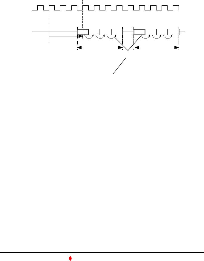
MITSUBISHI LSIs |
M2V64S20DTP-6,-6L,-7,-7L,-8,-8L |
(4-BANK x 4,194,304-WORD x |
4-BIT) |
||||||
SDRAM (Rev.3.2) |
M2V64S30DTP-6,-6L,-7,-7L,-8,-8L |
(4-BANK x 2,097,152-WORD x |
8-BIT) |
||||||
M2V64S40DTP-6,-6L,-7,-7L,-8,-8L |
(4-BANK x 1,048,576-WORD x 16-BIT) |
||||||||
|
Feb.'00 |
||||||||
|
|
|
64M Synchronous DRAM |
||||||
|
|
|
|
|
|||||
|
|
|
|
|
|
|
|
|
|
|
CLK |
|
|
|
|
|
|
||
|
|
|
|
|
|
|
|||
|
Command |
|
Read |
|
Write |
|
|
|
|
|
|
|
|
|
|
|
|
|
|
|
Address |
|
Y |
|
Y |
|
|
|
|
DQ
CL= 3
BL= 4
Q0 |
Q1 |
Q2 |
Q3 |
D0 |
D1 |
D2 |
D3 |
/CAS Latency
|
|
|
|
|
|
|
|
|
|
|
|
|
Burst Length |
|
|
|
|
Burst Length |
|
||
Burst Type
Initial Address |
BL |
|
|
|
|
|
|
|
|
Column Addressing |
|
|
|
|
|
|
|
|
|
||||||
|
|
|
|
|
|
|
|
|
|
|
|
|
|
|
|
|
|
|
|
|
|
|
|
|
|
A2 |
A1 |
A0 |
|
|
|
|
Sequential |
|
|
|
|
|
|
|
Interleaved |
|
|
|
|||||||
0 |
0 |
0 |
|
0 |
1 |
2 |
3 |
4 |
|
5 |
6 |
7 |
0 |
1 |
|
2 |
|
3 |
4 |
|
5 |
6 |
7 |
||
0 |
0 |
1 |
|
1 |
2 |
3 |
4 |
5 |
|
6 |
7 |
0 |
1 |
0 |
|
3 |
|
2 |
5 |
|
4 |
7 |
6 |
||
0 |
1 |
0 |
|
2 |
3 |
4 |
5 |
6 |
|
7 |
0 |
1 |
2 |
3 |
|
0 |
|
1 |
6 |
|
7 |
4 |
5 |
||
0 |
1 |
1 |
|
3 |
4 |
5 |
6 |
7 |
|
0 |
1 |
2 |
3 |
2 |
|
1 |
|
0 |
7 |
|
6 |
5 |
4 |
||
1 |
0 |
0 |
8 |
4 |
5 |
6 |
7 |
0 |
|
1 |
2 |
3 |
4 |
5 |
|
6 |
|
7 |
0 |
|
1 |
2 |
3 |
||
|
|
|
|
|
|||||||||||||||||||||
1 |
0 |
1 |
|
5 |
6 |
7 |
0 |
1 |
|
2 |
3 |
4 |
5 |
4 |
|
7 |
|
6 |
1 |
|
0 |
3 |
2 |
||
1 |
1 |
0 |
|
6 |
7 |
0 |
1 |
2 |
|
3 |
4 |
5 |
6 |
7 |
|
4 |
|
5 |
2 |
|
3 |
0 |
1 |
||
1 |
1 |
1 |
|
7 |
0 |
1 |
2 |
3 |
|
4 |
5 |
6 |
7 |
6 |
|
5 |
|
4 |
3 |
|
2 |
1 |
0 |
||
- |
0 |
0 |
|
0 |
1 |
2 |
3 |
|
|
|
|
|
|
0 |
1 |
|
2 |
|
3 |
|
|
|
|
|
|
- |
0 |
1 |
|
1 |
2 |
3 |
0 |
|
|
|
|
|
|
1 |
0 |
|
3 |
|
2 |
|
|
|
|
|
|
- |
1 |
0 |
4 |
2 |
3 |
0 |
1 |
|
|
|
|
|
|
2 |
3 |
|
0 |
|
1 |
|
|
|
|
|
|
|
|
|
|
|
|
|
|
|
|
|
|
|
|
|
|||||||||||
- |
1 |
1 |
|
3 |
0 |
1 |
2 |
|
|
|
|
|
|
3 |
2 |
|
1 |
|
0 |
|
|
|
|
|
|
|
|
|
|
|
|
|
|
|
|
|
|
|
|
|
|
|
|
|
|
|
|
|
|
|
|
- |
- |
0 |
|
0 |
1 |
|
|
|
|
|
|
|
|
0 |
1 |
|
|
|
|
|
|
|
|
|
|
- |
- |
1 |
2 |
1 |
0 |
|
|
|
|
|
|
|
|
1 |
0 |
|
|
|
|
|
|
|
|
|
|
|
|
|
|
|
|
|
|
|
|
|
|
|
|
|
|
|
|
|
|||||||
|
|
|
|
|
|
|
|
|
|
|
|
|
|
|
|
|
|
|
|
|
|
|
|
|
|
 MITSUBISHI ELECTRIC
16
 Loading...