


LX8585A-15CP
Microsemi Corporation LX8585A-15CP, LX8585A-15CDD, LX8585-33CP, LX8585-33CDD, LX8585-15CP Datasheet
...
DESCRIPTION KEY FEATURES
■ THREE-TERMINAL ADJUSTABLE OR FIXED
OUTPUT
■
GUARANTEED < 1.2V HEADROOM AT 4.6A
(LX8585A)
■
GUARANTEED < 1.4V HEADROOM AT 4.6A
(LX8585)
■ GUARANTEED < 1.3V HEADROOM AT 3A
■ OUTPUT CURRENT OF 4.6A MINIMUM
p FAST TRANSIENT RESPONSE
p 1% VOLTAGE REFERENCE INITIAL
ACCURACY
p OUTPUT SHORT CIRCUIT PROTECTION
p BUILT-IN THERMAL SHUTDOWN
The LX8585/85A Series ICs are low drop-
out three-terminal regulators with a mini-
mum of 4.6A output current. Pentium
®
Processor and Power PC
TM
applications
requiring fast transient response are ide-
ally suited for this product family. The
LX8585A is guaranteed to have < 1.2V
at 4.6A, while the LX8585 are specified
for 1.4V, making them ideal to provide
well regulated outputs of 2.5V to 3.6V
using a 5V input supply. Fixed versions
are also available and specified in the
Available Options table below.
Current limit is trimmed above 4.6A to
ensure adequate output current and con-
trolled short-circuit current. On-chip
thermal limiting provides protection
against any possible overload that would
create excessive junction temperatures.
The LX8585/85A family is available in
both through-hole and surface-mount
versions of the industry standard 3-pin
TO-220 / TO-263 power packages.
The LX1431 Programmable Reference
and LX8585A Series products offer pre-
cision output voltage and are ideal for
use in VRE applications (see application
below). For higher current applications,
see the LX8584 data sheet.
APPLICATIONS
■ PENTIUM PROCESSOR SUPPLIES
■ POWER PC SUPPLIES
■ MICROPROCESSOR SUPPLIES
■ LOW VOLTAGE LOGIC SUPPLIES
■ BATTERY POWERED CIRCUIT
■ POST REGULATOR FOR SWITCHING SUPPLY
■ CYRIX
®
6x86
TM
SUPPLIES
■ AMD-K5
TM
SUPPLIES
4.6A L
OW
D
ROPOUT
P
OSITIVE
R
EGULATORS
P RODUCTION DAT A SHEET
THE INFINITE POWER OF INNOVATION
LX8585-xx/8585A-xx
LIN DOC #:
8585
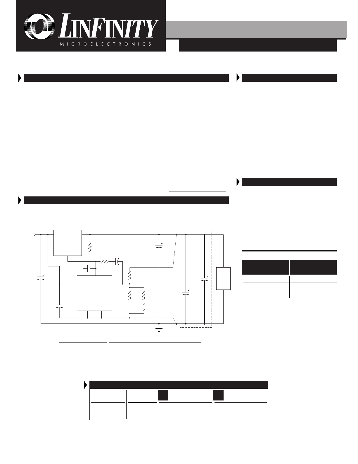
PRODUCT HIGHLIGHT
THE APPLICATION OF THE LX8585A & LX1431 IN A
75 & 166MHZ P54C PROCESSORS USING 5V CACHE
µP
Load
100µF x 6
10V
AVX TYPE
TPS
1µF x 10
SMD
1k
0.1%
2.84k
Ω
0.1%
COL
V
+
V
+
V
+
SGND FGND
REF
LX1431
V
IN
V
OUT
ADJ
1k
Ω
1k
Ω
0.01µF
2x
330µF, 6.3V
Low ESR
Oscon Type
from Sanyo
23
1
65
8
1
3
0.1µF
50V
220µF
10V
Low ESR
from
Sanyo
5V
PLACE IN µP SOCKET CAVITY
LX8585A
2
250pF
21k
1%
JP1
V
O
4.6A
(See Table Below)
Thick traces represent high current traces which must be low resistance / low
inductance traces in order to achieve good transient response.
V
OUT
JP1 TYPICAL APPLICATION
3.50 Short 120/166MHz, VRE, 5V Cache
3.38 Open 75/90/100/133MHz, STND, 5V Cache
PACKAGE ORDER INFORMATION
T
A
(°C)
Plastic TO-220
3-pin
P
Plastic T0-263
3-pin
DD
0 to 125 1.4V LX8585-xxCP LX8585-xxCDD
1.2V LX8585A-xxCP LX8585A-xxCDD
Dropout
Voltage
Note: All surface-mount packages are available in Tape & Reel. Append the letter "T" to part number. (i.e. LX8585A-00CDDT)
"xx" refers to output voltage, please see table above.
LX8585/85A-00 Adjustable
LX8585/85A-15 1.5V
LX8585/85A-33 3.3V
Part #
Output
Voltage
AVAILABLE OPTIONS PER PART #
Other voltage options may be available —
Please contact factory for details.
Copyright © 1997
Rev. 2.2 12/97
1
11861 WESTERN AVENUE, GARDEN GROVE, CA. 92841, 714-898-8121, FAX: 714-893-2570
L INFINITY MICROELECTRONICS INC.
IMPORTANT: For the most current data, consult LinFinity's web site: http://www.linfinity.com.
4.6A L
OW
D
ROPOUT
P
OSITIVE
R
EGULATORS
LX8585-xx/8585A-xx
PRODUCT DATABOOK 1996/1997
Copyright © 1997
Rev. 2.2 12/97
2
P
RODUCTION DATA SHEET
ABSOLUTE MAXIMUM RATINGS (Note 1)
Power Dissipation .................................................................................. Internally Limited
Input Voltage................................................................................................................ 10V
Input to Output Voltage Differential ........................................................................... 10V
Operating Junction Temperature
Plastic (P, DD Package) ........................................................................................ 150°C
Storage Temperature Range ...................................................................... -65°C to 150°C
Lead Temperature (Soldering, 10 seconds) ............................................................. 300°C
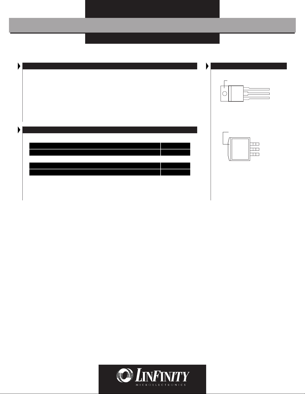
PACKAGE PIN OUTS
P PACKAGE
(Top View)
* Pin 1 is GND for fixed voltage versions.
3
2
1
V
IN
ADJ / GND*
V
OUT
DD PACKAGE
(Top View)
* Pin 1 is GND for fixed voltage versions.
Note 1. Exceeding these ratings could cause damage to the device. All voltages are with respect
to Ground. Currents are positive into, negative out of the specified terminal.
P PACKAGE:
THERMAL RESISTANCE-JUNCTION TO TAB,
θθ
θθ
θ
JT
3.0°C/W
THERMAL RESISTANCE-JUNCTION TO AMBIENT,
θθ
θθ
θ
JA
60°C/W
DD PACKAGE:
THERMAL RESISTANCE-JUNCTION TO TAB,
θθ
θθ
θ
JT
3.0°C/W
THERMAL RESISTANCE-JUNCTION TO AMBIENT,
θθ
θθ
θ
JA
60°C/W*
Junction Temperature Calculation: T
J
= T
A
+ (P
D
x θ
JA
). The θ
JA
numbers are guidelines for the
thermal performance of the device/pc-board system. All of the above assume no ambient airflow.
* θ
JA
can be improved with package soldered to 0.5IN
2
copper area over backside ground
plane or internal power plane. θ
JA
can vary from 20ºC/W to > 40ºC/W depending on
mounting technique.
THERMAL DATA
V
IN
V
OUT
ADJ / GND*
3
2
1
TAB IS V
OUT
TAB IS V
OUT
4.6A L
OW
D
ROPOUT
P
OSITIVE
R
EGULATORS
LX8585-xx/8585A-xx
PRODUCT DATABOOK 1996/1997
3
Copyright © 1997
Rev. 2.2 12/97
P RODUCTION DATA SHEET
Reference Voltage LX8585/85A V
REF
I
OUT
= 10mA, T
A
= 25°C
10mA ≤ I
OUT
≤ 4.6A, 1.5V ≤ (V
IN
- V
OUT
), V
IN
≤ 7V, P ≤ P
MAX
Line Regulation (Note 2)
∆V
REF
(V
IN
)
I
OUT
= 10mA, 1.5V ≤ (V
IN
- V
OUT
), V
IN
≤ 7V
Load Regulation (Note 2)
∆V
REF
(I
OUT
)
V
IN
- V
OUT
= 3V, 10mA ≤ I
OUT
≤ 4.6A
Thermal Regulation
∆V
OUT
(Pwr)
T
A
= 25°C, 20ms pulse
Ripple Rejection (Note 3) V
OUT
= 3.3V, f =120Hz, C
OUT
= 100µf Tantalum, V
IN
= 5V
C
ADJ
= 10µF, T
A
= 25°C, I
OUT
= 4.6A
Adjust Pin Current I
ADJ
Adjust Pin Current Change ∆I
ADJ
10mA ≤ I
OUT
≤ 4.6A, 1.5V ≤ (V
IN
- V
OUT
), V
IN
≤ 7V
Dropout Voltage LX8585 ∆V ∆V
REF
= 1%, I
OUT
= 4.6A
∆V
REF
= 1%, I
OUT
= 3A
LX8585A ∆V
REF
= 1%, I
OUT
= 4.6A
Minimum Load Current I
OUT(MIN)
V
IN
≤ 7V
Maximum Output Current (Note 4) I
OUT(MAX)
1.4V ≤ (V
IN
- V
OUT
), V
IN
≤ 7V
Temperature Stability (Note 3) ∆V
OUT
(t)
Long Term Stability (Note 3) ∆V
OUT
(t) T
A
= 125°C, 1000 hrs
RMS Output Noise (% of V
OUT
) (Note 3) V
OUT (RMS)
T
A
= 125°C, 10Hz £ f £ 10kHz
ELECTRICAL CHARACTERISTICS
(Unless otherwise specified, these specifications apply over the operating ambient temperatures for the LX8585-xxC/85A-xxC with 0°C ≤ T
A
≤ 125°C;
V
IN
- V
OUT
= 3V; I
OUT
= 4.6A. Low duty cycle pulse testing techniques are used which maintains junction and case temperatures equal to the ambient temperature.)
Parameter
Symbol
Test Conditions Units
LX8585/85A-00
Min. Typ. Max.
1.238 1.250 1.262 V
1.225 1.250 1.275 V
0.035 0.2 %
0.1 0.5 %
0.01 0.02 %/W
60 83 dB
55 100 µA
0.2 5 µA
1.2 1.4 V
1.1 1.3 V
1.1 1.2 V
210mA
4.6 6 A
0.25 %
0.3 1 %
0.003 %
Note 2. Regulation is measured at constant junction temperature, using pulse testing with a low duty cycle. Changes in output voltage due to heating
effects are covered under the specification for thermal regulation.
Note 3. These parameters, although guaranteed, are not tested in production.
Note 4. I
OUT (MAX)
is measured under the condition that V
OUT
is forced below its nominal value by 100mV.
Parameter
Symbol
Test Conditions Units
LX8585/85A-15
Min. Typ. Max.
Output Voltage (Note 4) V
OUT
V
IN
= 5V, I
OUT
= 0mA, T
A
= 25°C
4.75V ≤ V
IN
≤ 10V, 0mA ≤ I
OUT
≤ 7A, T
A
= 25°C, P ≤ P
MAX
Line Regulation (Note 2) ∆V
OUT
4.75V ≤ V
IN
≤ 7V
(V
IN
)
4.75V ≤ V
IN
≤ 10V
Load Regulation (Note 2)
∆V
OUT
(I
OUT
)
V
IN
= 5V, 10mA ≤ I
OUT
≤ I
OUT (MAX)
Thermal Regulation (Note 3)
∆V
OUT
(Pwr)
T
A
= 25°C, 20ms pulse
Ripple Rejection (Note 3) C
OUT
= 100µF (Tantalum), I
OUT
= 4.6A, T
A
= 25°C
Quiescent Current I
Q
0mA ≤ I
OUT
≤ I
OUT (MAX)
, 4.75V ≤ V
IN
≤ 10V
Dropout Voltage LX8585-15 ∆V ∆V
OUT
= 1%, I
OUT
≤ I
OUT (MAX)
, V
IN
- V
OUT
≤ 7V
∆V
OUT
= 1%, I
OUT
≤ 3A, V
IN
- V
OUT
≤ 7V
LX8585A-15 ∆V
OUT
= 1%, I
OUT
≤ I
OUT (MAX)
, V
IN
- V
OUT
≤ 7V
Temperature Stability (Note 3) ∆V
OUT
(T)
Long Term Stability (Note 3) ∆V
OUT
(t) T
A
= 125°C, 1000 hours
RMS Output Noise (% of V
OUT
) (Note 3) V
OUT (RMS)
T
A
= 25°C, 10Hz ≤ f ≤ 10kHz
1.485 1.50 1.515 V
1.470 1.50 1.530 V
13mV
15mV
2.5 7 mV
0.01 0.02 % / W
65 83 dB
410mA
1.2 1.4 V
1.1 1.3 V
1.1 1.2 V
0.25 %
0.3 1 %
0.003 %
LX8585-00 / 8585A-00 (Adjustable)
LX8585-15 / 8585A-15 (1.5V Fixed)
 Loading...