


Microsemi Corporation LX6431IDM, LX6431CLP, LX6431CDM, LX6431BILP, LX6431BIDM Datasheet
...
|
|
|
|
|
|
LX6431/LX6431A/LX6431B |
|
|
|
|
|
|
|
P R E C I S I O N P R O G R A M M A B L E R E F E R E N C E S |
|
|
|
|
|
T H E I N F I N I T E P O W E R O F I N N O V A T I O N |
P R O D U C T I O N D A T A S H E E T |
||
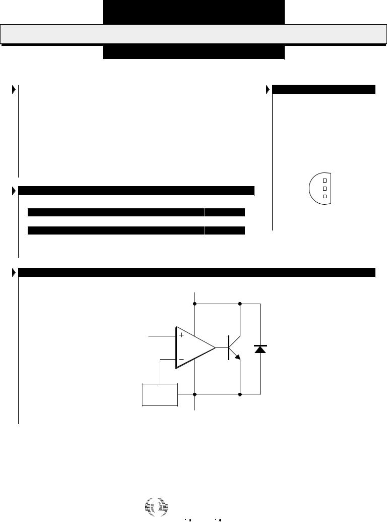
D E S C R I P T I O N
The LX6431 series precision adjustable three terminal shunt voltage regulators are pin-to-pin compatible with the industry standard TL431, but with significant improvements. The LX6431 design has eliminated regions of instability common to older generation shunt regulator products like the TL431. Designs are made simpler by eliminating the task of insuring capacitive loads, and output voltage and cathode currents don't combine for unstable operation. The capacitor value is chosen simply to give the best load transient response without the possibility of instability. A lower reference input current allows the use of higher value reference divider resistors,
reducing the current drain from batteries in portable equipment as well as reducing the voltage programming errors due to the impedance of the divider network (See Product Highlight figure below). In addition, the LX6431B has an improved initial accuracy of 0.4%, and the output voltage is programmable by using two external resistors from 2.5V to 36V.
These devices offer low output impedance for improved load regulation. The typical output impedance of these devices is 100mΩ . The reduced reference input bias current and minimum operating currents make these devices suitable for portable and micropower applications.
K E Y F E AT U R E S
■Unconditionally Stable For All Cathode To
Anode Capacitance Values
■Reduced Reference Input Current Allowing
The Use Of Higher Value Divider Resistors
(0.5µA Max.)
■Initial Voltage Reference Accuracy Of 0.4%
(LX6431B)
■Sink Current Capability 0.6mA to 100mA
■Typical Output Dynamic Impedance Less
Than 100mΩ
■Adjustable Output Voltage From 2.5V to
36V
NOTE: For current data & package dimensions, visit our web site: http://www.linfinity.com. |
|
|||||||||||
|
|
|
|
|
|
|
|
P R O D U C T H I G H L I G H T |
|
|||
|
|
|
O U T P U T V O L TA G E E R R O R D U E T O I R E F |
|
|
|||||||
|
20 |
|
|
|
|
|
|
|
|
|
T Y P I C A L P R O G R A M M A B L E V O L T A G E |
|
|
|
|
|
|
|
|
|
|
|
|
R E F E R E N C E C I R C U I T |
|
|
18 |
|
|
|
|
|
|
|
|
|
|
|
|
|
|
|
|
|
|
|
|
|
|
|
|
|
16 |
|
|
|
|
|
|
|
|
|
VIN |
VKA |
|
14 |
|
|
|
|
|
|
|
|
|
|
R1 |
Error |
12 |
|
|
|
|
|
|
|
|
|
|
|
|
|
|
|
|
|
|
|
|
|
|
||
10 |
|
|
|
|
|
|
|
|
|
|
LX6431 |
|
% |
|
|
|
|
|
|
|
|
|
|
||
8 |
|
|
|
|
|
|
|
|
|
|
|
|
|
|
|
|
|
|
|
|
|
|
|
R2 |
|
|
6 |
|
|
|
|
|
|
|
|
|
|
|
|
|
|
|
|
|
|
|
|
|
|
|
|
|
4 |
|
|
|
|
|
|
|
|
|
|
|
|
2 |
|
|
|
|
|
|
|
|
|
|
GND |
|
0 |
|
|
|
|
|
|
|
|
|
|
|
|
|
|
|
|
|
|
|
|
|
|
|
|
|
2.5 |
3.75 |
5 |
6.25 |
|
|
|
|
|
|
|
|
|
|
7.5 |
|
|
|
|
|
|
|
|||
|
|
|
|
|
|
|
|
|
|
|||
|
|
|
|
8.75 |
|
|
|
|
|
|
||
|
|
|
|
|
10 |
|
|
|
|
|
||
|
|
|
|
|
|
11.25 |
|
|
|
|
||
|
|
|
|
|
|
|
12.5 |
|
|
|
||
|
|
|
|
|
|
|
|
13.75 |
|
|
||
|
|
|
|
(VKA) |
Output Voltage - (V) |
15 |
|
|||||
|
|
|
|
|
|
|||||||
|
|
|
|
|
|
|
||||||
|
|
|
|
|
|
PA C K A G E O R D E R I N F O R M AT I O N |
|
|||||
|
|
|
|
Initial |
|
|
Plastic SOIC |
|
Plastic TO-92 |
|
|
|
TA (°C) |
|
|
DM |
LP |
|
|||||
|
|
|
|
Tolerance |
|
|
8-pin |
|
3-pin |
|
|
|
|
|
|
|
|
|
|
|
|
|
|
|
|
|
|
2% |
|
|
LX6431CDM |
|
LX6431CLP |
|
|
|
0 to 70 |
|
1% |
|
|
LX6431ACDM |
|
LX6431ACLP |
|
||
|
|
|
|
0.4% |
|
|
LX6431BCDM |
|
LX6431BCLP |
|
|
|
|
|
|
2% |
|
|
LX6431IDM |
|
LX6431ILP |
|
|
|
-40 to 85 |
|
1% |
|
|
LX6431AIDM |
|
LX6431AILP |
|
||
|
|
|
|
0.4% |
|
|
LX6431BIDM |
|
LX6431BILP |
|
|
Copyright © 1999
Rev. 1.4 6/99
Note: All surface-mount packages are available in Tape & Reel.
Append the letter "T" to part number. (i.e. LX5212CDPT)
TO-92 (LP) package also available in ammo-pack.
L I N F I N I T Y M I C R O E L E C T R O N I C S I N C . |
1 |
11861 WESTERN AVENUE, GARDEN GROVE, CA. 92841, 714-898-8121, FAX: 714-893-2570 |
P R O D U C T D A T A B O O K 1 9 9 6 / 1 9 9 7
LX6431/LX6431A/LX6431B
P R E C I S I O N P R O G R A M M A B L E R E F E R E N C E S
P R O D U C T I O N D A T A S H E E T
ABSOLUTE MAXIMUM RATINGS |
(Note 1) |
|
Cathode to Anode Voltage (VKA) ................................................................... |
-0.3V to 37V |
|
Reference Input Current (IREF) .................................................................... |
-50µA to 10µA |
|
Continuous Cathode Current (IK) ......................................................... |
-100mA to 150mA |
|
Operating Junction Temperature |
|
|
Plastic (DM & LP Packages) ................................................................................. |
150°C |
|
Storage Temperature Range ...................................................................... |
-65°C to 150°C |
|
Lead Temperature ..................................................................................................... |
300°C |
Note 1. Exceeding these ratings could cause damage to the device. All voltages are with respect to Ground. Currents are positive into, negative out of the specified terminal. Pin numbers refer to DIL packages only.
THERMAL DATA
DM PACKAGE:
THERMAL RESISTANCE-JUNCTION TO AMBIENT, θ JA |
165°C/W |
LP PACKAGE: |
|
THERMAL RESISTANCE-JUNCTION TO AMBIENT, θ JA |
156°C/W |
PACKAGE PIN OUTS
CATHODE |
|
|
|
1 |
8 |
|
|
REF |
N.C. |
|
|
|
2 |
7 |
|
|
ANODE |
|
|
|
|
|||||
ANODE |
|
|
|
3 |
6 |
|
|
ANODE |
|
|
|
|
|||||
N.C. |
|
|
|
4 |
5 |
|
|
N.C. |
|
|
|
|
|||||
|
|
|
|
|
|
|
|
|
DM PACKAGE
(Top View)
1. CATHODE
2. ANODE
3. REF
LP PACKAGE
(Top View)
Junction Temperature Calculation: TJ = TA + (PD x θ JA).
The θ JA numbers are guidelines for the thermal performance of the device/pc-board system. All of the above assume no ambient airflow
BLOCK DIAGRAM
Cathode (K)
Ref (R)
VREF
Anode (A)
2 |
|
Copyright © 1999 |
|
Rev. 1.4 6/99 |
|
|
|
|
P R O D U C T D A T A B O O K 1 9 9 6 / 1 9 9 7
LX6431/LX6431A/LX6431B
P R E C I S I O N P R O G R A M M A B L E R E F E R E N C E S
P R O D U C T I O N D A T A S H E E T
E L E C T R I C A L C H A R A C T E R I S T I C S (Note 2)
(Unless otherwise specified, these specifications apply over the operating ambient temperatures for LX6431C/LX6431AC/LX6431BC with 0°C ≤ TA ≤ 70°C, LX6431I/LX6431AI/LX6431BI with -40°C ≤ TA ≤ 85°C.)
|
Parameter |
|
Symbol |
Test Conditions |
LX6431 |
|
Units |
||||
|
|
Min. Typ. Max. |
|||||||||
|
|
|
|
|
|
|
|
|
|
||
Reference Input Voltage |
LX6431 |
VREF |
IK = 10mA, VKA = VREF, TA = 25°C, |
2440 |
|
|
2550 |
mV |
|||
|
|
|
|
LX6431A |
|
IK = 10mA, VKA = VREF, TA = 25°C |
2470 |
|
|
2520 |
mV |
|
|
|
|
LX6431B |
|
IK = 10mA, VKA = VREF, TA = 25°C |
2490 |
|
|
2510 |
mV |
Reference Drift |
|
LX6431 |
|
IK = 10mA, VKA = VREF, 0°C ≤ TA ≤ 70°C |
|
|
|
15 |
mV |
||
|
|
|
|
|
|
IK = 10mA, VKA = VREF, -40°C ≤ TA ≤ 85°C |
|
|
|
25 |
mV |
|
|
|
|
LX6431A |
|
IK = 10mA, VKA = VREF, 0°C ≤ TA ≤ 70°C |
|
|
|
15 |
mV |
|
|
|
|
|
|
IK = 10mA, VKA = VREF, -40°C ≤ TA ≤ 85°C |
|
|
|
25 |
mV |
|
|
|
|
LX6431B |
|
IK = 10mA, VKA = VREF, 0°C ≤ TA ≤ 70°C |
|
|
|
15 |
mV |
|
|
|
|
|
|
IK = 10mA, VKA = VREF, -40°C ≤ TA ≤ 85°C |
|
|
|
20 |
mV |
Voltage Ratio, Reference to Cathode |
|
IK = 10mA, VKA = 2.5V to 36V, TA = 25°C |
|
0.3 |
|
1 |
mV/V |
||||
(Note 3) |
|
|
|
IK = 10mA, VKA = 2.5V to 36V, TA = Operating Range |
|
0.3 |
|
1 |
mV/V |
||
Reference Input Current |
|
IREF |
VKA = VREF, TA = 25°C |
|
0.1 |
|
0.5 |
µA |
|||
|
|
|
|
|
|
VKA = VREF, TA = Operating Range |
|
0.1 |
|
0.5 |
µA |
Minimum Operating Current |
|
IMIN |
VKA = VREF to 36V, TA = 25°C |
|
0.4 |
|
0.6 |
mA |
|||
|
|
|
|
|
|
VKA = VREF to 36V, TA = Operating Range |
|
0.4 |
|
0.6 |
mA |
Off-State Cathode Current |
|
IOFF |
VKA = 36V, VREF = 0V, TA = 25°C |
|
0.3 |
|
1 |
µA |
|||
Dynamic Impedance |
|
ZKA |
VKA = VREF, IK = 0.6mA to 100mA, f ≤ 1kHz, TA = 25°C |
|
30 |
|
100 |
mΩ |
|||
Note 2. These parameters are guaranteed by design. |
|
|
|
|
|
|
|
||||
Note 3. |
∆ VREF |
|
Ratio of change in reference input voltage |
|
|
|
|
|
|
||
∆ VKA |
|
|
|
|
|
|
|||||
|
to the change in cathode voltage. |
|
|
|
|
|
|
|
|||
Copyright © 1999 |
3 |
Rev. 1.4 6/99 |
P R O D U C T D A T A B O O K 1 9 9 6 / 1 9 9 7
LX6431/LX6431A/LX6431B
P R E C I S I O N P R O G R A M M A B L E R E F E R E N C E S
P R O D U C T I O N D A T A S H E E T
GRAPH / CURVE INDEX
Characteristic Curves
FIGURE #
1.REFERENCE VOLTAGE vs. FREE-AIR TEMPERATURE
2.REFERENCE CURRENT vs. FREE-AIR TEMPERATURE
3.CATHODE CURRENT vs. CATHODE VOLTAGE
4.OFF-STATE CATHODE CURRENT vs. FREE-AIR TEMPERATURE
5.RATIO OF DELTA REFERENCE VOLTAGE TO DELTA CATHODE VOLTAGE vs. FREE-AIR TEMPERATURE
6.EQUIVALENT INPUT NOISE VOLTAGE vs. FREQUENCY
FIGURE INDEX
Application Information
FIGURE #
7.COMPARISON OF REFERENCE RESISTOR VALUES BETWEEN AN LX6431B AND A TL1431. Resistors used with the LX6431B are 5 times higher in value.
8.COMPARISON OF REFERENCE RESISTOR VALUES BETWEEN AN LX6431B AND A TL1431. When used as 0.5%, 5V shunt regulators.
Parameter Measurement Information
FIGURE #
9.TEST CIRCUIT FOR VKA = VREF
10.TEST CIRCUIT FOR VKA > VREF
11.TEST CIRCUIT FOR IOFF
Typical Characteristics
FIGURE #
12.EQUIVALENT INPUT NOISE VOLTAGE OVER A 10-SECOND PERIOD
13.SMALL-SIGNAL VOLTAGE AMPLIFICATION vs. FREQUENCY
14.REFERENCE IMPEDANCE vs. FREQUENCY
15.PULSE RESPONSE
16.DIFFERENTIAL VOLTAGE AMPLIFICATION vs. FREQUENCY
4 |
|
Copyright © 1999 |
|
Rev. 1.4 6/99 |
|
|
|
|
 Loading...