


Microsemi Corporation LX8584B-33CV, LX8584B-00CP, LX8584A-33CV, LX8584A-33CP, LX8584A-00CV Datasheet
...
|
|
LIN D O C #: 8584 |
|
|
|
|
|
|
|
|
LX8584-xx/8584A-xx/8584B-xx |
|
|
|
|
|
|
|
|
|
|
7 A L O W D R O P O U T P O S I T I V E R E G U L A T O R S |
|
|
|
|
|
|
|
T H E I N F I N I T E P O W E R O F I N N O V A T I O N |
|
P R O D U C T I O N D A T A S H E E T |
|
|
D E S C R I P T I O N
The LX8584/84A/84B series ICs are low dropout three-terminal positive regulators with a nominal 7A output current. This product family is ideally suited for Pentium® Processor and Power PCTM applications requiring fast transient response. The LX8584A isguaranteed to have < 1.2V at 7A and the LX8584/84B < 1.4V at 7A dropout voltage, making them ideal to provide well regulated outputs of 2.5V to 3.6V using a 5V input supply. In addition, the LX8584B also offers ±1% maximum voltage reference accuracy over temperature. Fixed versions are also available and are specified in the Available Options table below.
Current limit is trimmed above 7.1A to ensure adequate output current and controlled short-circuit current. On-chip thermal limiting provides protection against any combination of overload that would create excessive junction temperatures.
The LX8584/84A series products are available in both the through-hole versions of the industry standard 3-pin TO-220 and TO-247 power packages.
The LX1431 Programmable Reference in conjunction with the LX8584 7A LDO products offer precision output voltage (see application below) and are ideal for use in VRE applications.
K E Y F E AT U R E S
■THREE-TERMINAL ADJUSTABLE OR FIXED OUTPUT
■GUARANTEED 1% VOLTAGE ACCURACY OVER TEMPERATURE (LX8584B)
■GUARANTEED ≤ 1.2V HEADROOM AT 7A (LX8584A)
■GUARANTEED ≤ 1.4V HEADROOM AT 7A (LX8584/84B)
■OUTPUT CURRENT OF 7A
pFAST TRANSIENT RESPONSE
p1% VOLTAGE REFERENCE INITIAL
ACCURACY
pOUTPUT SHORT CIRCUIT PROTECTION
pBUILT-IN THERMAL SHUTDOWN
■EVALUATION BOARD AVAILABLE: REQUEST LXE9001 EVALUATION KIT
|
|
|
P R O D U C T H I G H L I G H T |
|
|
|||
|
THE APPLICATION OF THE LX8584A & LX1431 IN A |
|
||||||
|
75 & 166MHZ P54C PROCESSORS USING 3.3V CACHE |
|
||||||
|
3 |
|
2 |
|
|
VO 7A |
PLACE IN µP SOCKET CAVITY |
|
5V |
|
|
|
(See Table Below) |
|
|
||
VIN |
VOUT |
|
|
3x |
|
|
||
|
LX8584A |
|
|
|
|
|
||
|
1k |
|
330µF, 6.3V |
|
|
|||
|
|
|
|
Low ESR |
|
|
||
|
ADJ |
|
|
1k |
0.01µF |
Oscon Type |
|
|
|
|
|
|
from Sanyo |
|
|
||
|
1 |
|
|
|
100µF x 6 |
|
||
|
|
|
250pF |
|
|
|
|
|
|
|
|
|
|
|
10V |
|
|
|
|
|
2 |
1 |
|
1k |
AVX TYPE |
|
|
|
|
|
TPS |
µP |
|||
|
|
|
|
COL |
|
0.1% |
||
|
220µF |
3 |
|
8 |
|
Load |
||
|
V+ |
REF |
|
|
||||
|
10V |
|
|
|
|
|
|
|
|
Low ESR |
|
LX1431 |
2.84k |
21k |
|
|
|
|
from |
|
1µF x 10 |
|
||||
|
Sanyo |
|
|
|
0.1% |
1% |
|
|
|
|
|
|
|
|
SMD |
|
|
|
0.1µF |
|
|
|
|
JP1 |
|
|
|
|
SGND |
FGND |
|
|
|
||
|
50V |
|
|
|
|
|||
|
|
|
|
|
|
|||
|
|
|
5 |
6 |
|
|
|
|
|
VOUT |
|
JP1 |
|
TYPICAL APPLICATION |
|
||
3.50 |
Short |
120/166MHz, VRE, 3.3V Cache |
3.38 |
Open |
75/90/100/133MHz, STND, 3.3V Cache |
Thick traces represent high current traces which must be low resistance / low inductance in order to achieve good transient response.
PA C K A G E O R D E R I N F O R M AT I O N
TA (°C) |
|
Dropout |
P |
Plastic TO-220 |
|
V |
Plastic TO-247 |
||
|
|
|
Voltage |
|
3-pin |
|
|
3-terminal |
|
|
|
|
|
|
|
|
|
|
|
|
|
|
1.4V |
|
LX8584-xxCP |
|
|
LX8584-xxCV |
|
|
|
|
|
|
|
|
|
||
0 to 125 |
|
LX8584B-xxCP |
|
|
LX8584B-xxCV |
||||
|
|
|
|
|
|
||||
|
|
|
1.2V |
|
LX8584A-xxCP |
|
|
LX8584A-xxCV |
|
"xx" refers to output voltage, please see table above.
A P P L I C AT I O N S
■PENTIUM PROCESSOR SUPPLIES
■POWER PC SUPPLIES
■MICROPROCESSOR SUPPLIES
■LOW VOLTAGE LOGIC SUPPLIES
■POST REGULATOR FOR SWITCHING SUPPLY
D R O P O U T VO L TA G E V S.
O U T P U T C U R R E N T
|
|
1.5 |
|
|
|
|
|
|
|
|
|
|
|
|
|
|
|
|
|
|
|
|
|
|
|
|
|
|
|
|
|
|
|
|
|
|
|
|
|
|
|
LX8584/84A |
|
|
|
|
|
|
TJ = 125°C |
|
||||||
- (V) |
|
|
|
|
|
|
|
|
|
|
|
|
|
|
|
|
|
|
|
|
|
|
|
|
|
|
|
|
|
|
|
|
|
|
|
||
Differential |
|
|
|
|
|
|
|
|
|
|
|
|
|
|
|
|
|
|
|
|
|
|
|
|
|
|
|
|
|
|
|
|
|
|
|||
|
|
|
|
|
|
|
|
|
LX8584 |
|
|
|
|
|
|
|
||
1.0 |
|
|
|
|
|
|
|
|
|
|
|
|
|
|
|
|
||
|
|
|
|
|
|
|
|
|
|
|
|
|
|
|
|
|||
|
|
|
|
|
|
|
|
|
|
|
|
|
|
|
|
|||
Input / Output |
|
|
|
|
|
|
|
|
|
|
|
|
|
|
|
|
||
|
|
|
|
|
|
|
|
|
|
|
|
LX8584A |
|
|
||||
0.5 |
|
|
|
|
|
|
|
|
|
|
|
|
|
|
|
|
||
|
|
|
|
|
|
|
|
|
|
|
|
|
|
|
|
|||
|
|
|
|
|
|
|
|
|
|
|
|
|
|
|
|
|||
|
|
|
|
|
|
|
|
|
|
|
|
|
|
|
|
|||
|
|
|
|
|
|
|
|
|
|
|
|
|
|
|
|
|
|
|
|
|
|
|
|
|
|
|
|
|
|
|
|
|
|
|
|
|
|
|
|
|
|
|
|
|
|
|
|
|
|
|
|
|
|
|
|
|
|
|
0 |
1.75 |
|
|
3.5 |
5.25 |
|
|
|
7 |
|||||||
|
|
|
|
|
Output Current - (A) |
|
||||||||||||
|
|
|
|
|
|
|
||||||||||||
|
AVA I L A B L E O P T I O N S P E R PA R T # |
|
||||||||||||||||
|
|
|
|
|
|
|
|
|
|
|||||||||
|
|
Part # |
|
|
|
|
Output Voltage |
|
|
|
|
|||||||
|
|
|
|
|
|
|
|
|||||||||||
|
|
LX8584/A/B-00 |
|
|
Adjustable |
|
||||||||||||
|
|
|
|
|||||||||||||||
|
|
|
|
|
|
|
|
|
|
|||||||||
|
|
LX8584/A/B-33 |
|
|
|
|
3.3V |
|
|
|||||||||
Other voltage options may be available — Please contact factory for details.
F O R F U R T H E R I N F O R M AT I O N C A L L ( 7 1 4 ) 8 9 8 - 8 1 2 1
Copyright © 1997 |
11861 WESTERN AVENUE, GARDEN GROVE, CA. 92841 |
1 |
Rev. 1.2 4/97 |
|
|
P R O D U C T D A T A B O O K 1 9 9 6 / 1 9 9 7
LX8584-xx/8584A-xx/8584B-xx
7 A L O W D R O P O U T P O S I T I V E R E G U L A T O R S
P R O D U C T I O N D A T A S H E E T
ABSOLUTE MAXIMUM RATINGS |
(Note 1) |
|
Power Dissipation .................................................................................. |
Internally Limited |
|
Input Voltage ................................................................................................................ |
10V |
|
Input to Output Voltage Differential ........................................................................... |
10V |
|
Maximum Output Current ............................................................................................. |
8A |
|
Operating Junction Temperature |
|
|
Plastic (P Package) ................................................................................................ |
150°C |
|
Storage Temperature Range ...................................................................... |
-65°C to 150°C |
|
Lead Temperature (Soldering, 10 seconds) ............................................................. |
300°C |
Note 1. Exceeding these ratings could cause damage to the device. All voltages are with respect to Ground. Currents are positive into, negative out of the specified terminal.
THERMAL DATA
P PACKAGE:
THERMAL RESISTANCE-JUNCTION TO TAB, θJT |
2.7°C/W |
THERMAL RESISTANCE-JUNCTION TO AMBIENT, θJA |
60°C/W |
V PACKAGE: |
|
THERMAL RESISTANCE-JUNCTION TO TAB, θJT |
1.6°C/W |
THERMAL RESISTANCE-JUNCTION TO AMBIENT, θJA |
35°C/W |
Junction Temperature Calculation: TJ = TA + (PD x θJA).
The θJA numbers are guidelines for the thermal performance of the device/pc-board system. All of the above assume no ambient airflow.
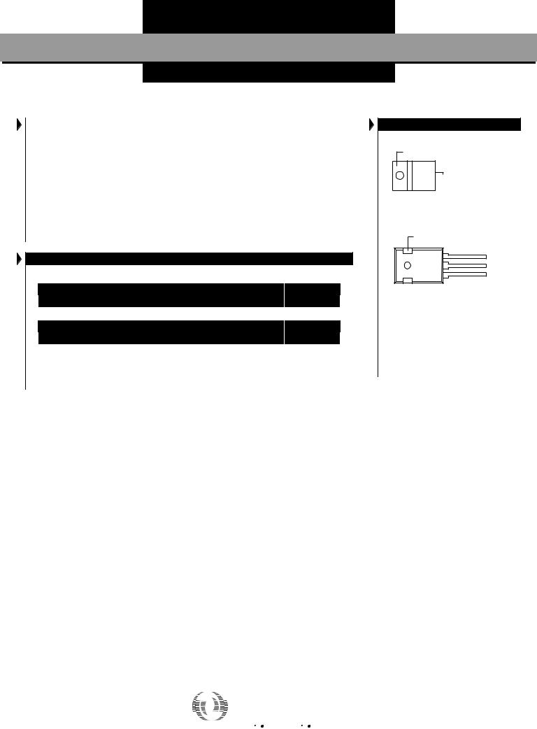
PACKAGE PIN OUTS
TAB IS VOUT
3  VIN
VIN
2 
 VOUT
VOUT
1  ADJ / GND*
P PACKAGE
(Top View)
* Pin 1 is GND for fixed voltage versions.
TAB ON REVERSE SIDE IS VOUT |
|
3 |
VIN |
2 |
VOUT |
1 |
ADJ / GND* |
V PACKAGE
(Top View)
* Pin 1 is GND for fixed voltage versions.
2 |
|
Copyright © 1997 |
|
Rev. 1.2 4/97 |
|
|
|
|

P R O D U C T D A T A B O O K 1 9 9 6 / 1 9 9 7
LX8584-xx/8584A-xx/8584B-xx
7 A L O W D R O P O U T P O S I T I V E R E G U L A T O R S
P R O D U C T I O N D A T A S H E E T
E L E C T R I C A L C H A R A C T E R I S T I C S
(Unless otherwise specified, these specifications apply over the operating ambient temperatures for the LX8584-xxC/84A-xxC/84B-xxC with 0°C ≤ TA ≤ 125°C; VIN - VOUT = 3V; IOUT = 7A. Low duty cycle pulse testing techniques are used which maintains junction and case temperatures equal to the ambient temperature.)
LX8584-00/84A-00/84B-00 (Adjustable)
Parameter |
Symbol |
Test Conditions |
LX8584/84A/84B-00 |
Units |
||||
Min. |
Typ. |
Max. |
||||||
|
|
|
|
|
||||
|
|
|
|
|
|
|
|
|
Reference Voltage |
LX8584/84A-00 |
VREF |
IOUT = 10mA, TA = 25°C |
1.238 |
1.250 |
1.263 |
V |
|
|
|
|
10mA ≤ IOUT ≤ 7A, 1.5V ≤ (VIN - VOUT), VIN ≤ 7V, P ≤ PMAX |
1.225 |
1.250 |
1.275 |
V |
|
|
LX8584B-00 |
|
IOUT = 10mA, TA = 25°C |
1.240 |
1.250 |
1.260 |
V |
|
|
|
|
10mA ≤ IOUT ≤ 7A, 1.5V ≤ (VIN - VOUT), VIN ≤ 7V, P ≤ PMAX |
1.238 |
1.250 |
1.263 |
V |
|
Line Regulation (Note 2) |
VREF (VIN) |
IOUT = 10mA, 1.5V ≤ (VIN - VOUT), VIN ≤ 7V |
|
0.035 |
0.2 |
% |
||
Load Regulation (Note 2) |
VREF (IOUT) |
VIN - VOUT = 3V, 10mA ≤ IOUT ≤ 7A |
|
0.1 |
0.5 |
% |
||
Thermal Regulation |
|
VOUT(Pwr) |
TA = 25°C, 20ms pulse |
|
0.01 |
0.02 |
%/W |
|
Ripple Rejection (Note 3) |
|
VOUT = 3.3V, f =120Hz, COUT = 100µf Tantalum, VIN = 5V |
65 |
83 |
|
dB |
||
|
|
|
CADJ = 10µF, IOUT = 7A |
|
|
|
|
|
Adjust Pin Current |
|
IADJ |
|
|
55 |
100 |
µA |
|
Adjust Pin Current Change |
IADJ |
10mA ≤ IOUT ≤ 7A, 1.5V ≤ (VIN - VOUT), VIN ≤ 7V |
|
0.2 |
5 |
µA |
||
Dropout Voltage |
LX8584A |
V |
VREF = 1%, IOUT = 7A |
|
1.1 |
1.2 |
V |
|
|
LX8584/84B |
|
VREF = 1%, IOUT = 7A |
|
1.2 |
1.4 |
V |
|
|
LX8584/84B |
|
VREF = 1%, IOUT = 6A |
|
1.1 |
1.3 |
V |
|
Minimum Load Current |
|
IOUT(MIN) |
VIN ≤ 7V |
|
2 |
10 |
mA |
|
Maximum Output Current |
IOUT (MAX) |
1.4V ≤ (VIN - VOUT), VIN ≤ 7V |
7 |
8 |
|
A |
||
Temperature Stability |
|
VOUT (T) |
|
|
0.25 |
|
% |
|
Long Term Stability |
|
VOUT (t) |
TA = 125°C, 1000 hrs |
|
0.3 |
1 |
% |
|
RMS Output Noise (% of VOUT) |
VOUT (RMS) |
TA = 25°C, 10Hz ≤ f ≤ 10kHz |
|
0.003 |
|
% |
||
LX8584-33/84A-33/84B-33 (3.3V Fixed)
Parameter |
Symbol |
|
Test Conditions |
LX8584/84A/84B-33 |
Units |
||||
|
Min. |
Typ. |
Max. |
||||||
|
|
|
|
|
|
|
|||
|
|
|
|
|
|
|
|
|
|
Output Voltage |
|
LX8584/84A-33 |
VOUT |
VIN = 5V, IOUT = 0mA, TA = 25°C |
3.267 |
3.30 |
3.333 |
V |
|
|
|
|
|
4.75V ≤ VIN ≤ 10V, 0mA ≤ IOUT ≤ 7A, P ≤ PMAX |
3.234 |
3.30 |
3.366 |
V |
|
|
|
LX8584B-33 |
|
VIN = 5V, IOUT = 0mA, TA = 25°C |
3.274 |
3.30 |
3.326 |
V |
|
|
|
|
|
4.75V ≤ VIN ≤ 10V, 0mA ≤ IOUT ≤ 7A, P ≤ PMAX |
3.267 |
3.30 |
3.333 |
V |
|
Line Regulation (Note 2) |
(VIN) |
VOUT |
4.75V ≤ VIN ≤ 7V |
|
1 |
6 |
mV |
||
|
|
|
4.75V ≤ VIN ≤ 10V |
|
2 |
10 |
mV |
||
Load Regulation (Note 2) |
|
VOUT (IOUT) |
VIN = 5V, 0mA ≤ IOUT ≤ IOUT (MAX) |
|
5 |
15 |
mV |
||
Thermal Regulation |
|
|
VOUT(Pwr) |
TA = 25°C, 20ms pulse |
|
0.01 |
0.02 |
% / W |
|
Ripple Rejection (Note 3) |
|
COUT = 100µF (Tantalum), IOUT = 7.5V |
60 |
83 |
|
dB |
|||
Quiescent Current |
|
|
IQ |
0mA ≤ IOUT ≤ IOUT (MAX) , 4.75V ≤ VIN ≤ 10V |
|
4 |
10 |
mA |
|
Dropout Voltage |
|
LX8584-xx |
V |
VOUT = 1%, IOUT = IOUT (MAX) |
|
|
1.4 |
V |
|
|
|
LX8584A-xx |
|
VOUT = 1%, IOUT = IOUT (MAX) |
|
|
1.2 |
V |
|
|
|
LX8584B-xx |
|
VOUT = 1%, IOUT = IOUT (MAX) |
|
|
1.4 |
V |
|
Maximum Output Current |
|
IOUT (MAX) |
VIN ≤ 7V |
` 7 |
8 |
|
A |
||
Temperature Stability (Note 3) |
VOUT (T) |
|
|
|
0.25 |
|
% |
||
Long Term Stability |
(Note 3) |
VOUT (t) |
TA = 125°C, 1000 hours |
|
0.3 |
1 |
% |
||
RMS Output Noise (% of VOUT) (Note 3) |
VOUT (RMS) |
TA = 25°C, 10Hz ≤ f ≤ 10kHz |
|
0.003 |
|
% |
|||
Note 2. Regulation is measured at constant junction temperature, using pulse testing with a low duty cycle. Changes in output voltage due to heating effects are covered under the specification for thermal regulation.
Note 3. These parameters, although guaranteed, are not tested in production.
Copyright © 1997 |
3 |
Rev. 1.2 4/97 |
 Loading...