


Microsemi Corporation LX1665CN, LX1665CDW, LX1665ACN, LX1665ACDW, LX1664CN Datasheet
...
|
|
|
|
|
|
LX1664/64A, LX1665/65A |
|
|
|
|
|
|
|
DUAL OUTPUT PWM CONTROLLERS WITH 5-BIT DAC |
|
|
|
|
|
T H E I N F I N I T E P O W E R O F I N N O V A T I O N |
P R O D U C T I O N D A T A S H E E T |
||
D E S C R I P T I O N
The LX1664/64A and LX1665/65A are monolithic switching regulator controller IC’s designed to provide a low cost, high performance adjustable power supply for advanced microprocessors and other applications requiring a very fast transient response and a high degree of accuracy.
Short-circuit Current Limiting without Expensive Current Sense Resistors.
Current-sensing mechanism can use PCB trace resistance or the parasitic resistance of the main inductor. The LX1664A and LX1665A have reduced current sense comparator threshold for optimum performance using a sense resistor. For applications requiring a high degree of accuracy, a conventional sense resistor can be used to sense current.
Programmable Synchronous Rectifier Driver for CPU Core. The main output is adjustable from 1.3V to 3.5V using a 5-bit code. The IC can read a VID signal
set by a DIP switch on the motherboard, or hardwired into the processor’s package (as in the case of Pentium® Pro and Pentium II processors). The 5-bit code adjusts the output voltage between 1.30 and 2.05V in 50mV increments and between 2.0 and 3.5V in 100mV increments, conforming to the Intel Corporation specification. The device can drive dual MOSFET’s resulting in typical efficiencies of 85 - 90% even with loads in excess of 10 amperes. For cost sensitive applications, the bottom MOSFET can be replaced with a Schottky diode (non-syn- chronous operation).
Linear Regulator Driver. The LX1664/ 65 family of devices have a secondary regulator output. This can drive a MOSFET or bipolar transistor as a pass element to construct a low-cost adjustable linear regulator suitable for powering a 1.5V GTL+ bus or 2.5V clock supply.
(continued next page)
IMPORTANT: For the most current data, consult LinFinity's web site: http://www.linfinity.com.
K E Y F E AT U R E S
■5-bit Programmable Output For CPU Core
Supply
■Adjustable Linear Regulator Driver Output
■No Sense Resistor Required For Short-
Circuit Current Limiting
■Designed To Drive Either Synchronous Or
Non-Synchronous Output Stages
■Soft-Start Capability
■Modulated, Constant Off-Time Architecture
For Fast Transient Response And Simple
System Design
■Available Over-Voltage Protection (OVP) Crowbar Driver And Power Good Flag
(LX1665 only)
A P P L I C AT I O N S
■Socket 7 (Pentium Class) Microprocessor
Supplies (including Intel Pentium Processor, AMD-K6TM And Cyrix® 6x86TM, Gx86TM and M2TM Processors)
■Pentium II and Deschutes Processor & L2-
Cache Supplies
■Voltage Regulator Modules
|
|
|
|
P R O D U C T H I G H L I G H T |
|
|
|
|
|
|
||||
|
|
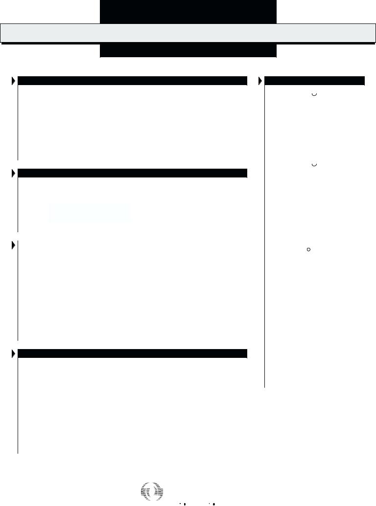
LX1665 I N A |
PE N T I U M |
II SI N G L E -CH I P PO W E R |
SU P P LY |
SO L U T I O N |
|
|
|
|||||
|
|
|
|
|
12V |
F1 20A |
5V |
|
|
|
|
|
|
|
|
|
|
|
|
|
|
|
|
|
|
|
|||
C3 |
|
|
|
|
|
L2 |
|
|
|
|
|
|
|
|
|
|
|
|
|
1µH |
|
6.3V |
|
|
|
|
|
|
|
0.1µF |
|
|
|
|
|
|
|
|
|
|
|
|
||
|
|
U1 |
|
|
C5 |
|
|
|
|
|
|
|
||
|
|
|
|
|
|
1500µF x3 |
|
|
|
|
|
|||
|
|
|
LX1665 |
|
1µF |
|
|
|
|
|
|
|||
|
|
1 |
18 |
|
Q1 |
C2 |
|
R1 |
|
|
|
|
||
|
|
SS |
VC1 |
|
|
|
|
Supply Voltage |
|
|
||||
|
|
2 |
INV |
TDRV |
17 |
|
IRL3102 |
L1 |
0.0025 |
|
|
|||
|
|
|
|
for CPU Core VOUT |
|
|||||||||
|
|
3 |
16 |
|
|
2.5µH |
|
|
|
|
||||
|
|
4 |
VCC_CORE |
GND |
15 |
|
Q2 |
|
|
|
C |
|
|
|
VID0 |
|
VID0 |
BDRV |
|
|
|
|
|
|
|
||||
|
|
|
|
IRL3303 |
|
|
|
|
1 |
|
|
|||
VID1 |
|
5 |
VID1 |
VCC |
14 |
|
|
|
|
|
6.3V, 1500µF x 3** |
|
||
|
6 |
13 |
|
|
|
C9 |
|
|
** Three capacitors for Pentium |
|||||
VID2 |
|
VID2 |
CT |
|
|
|
|
|
Four capacitors for Pentium II |
|||||
|
|
|
C8 |
|
|
330µF |
|
|
|
|
||||
VID3 |
|
7 |
VID3 |
OV 12 |
|
|
|
|
|
|
||||
|
Q4 |
|
|
|
|
|
|
|
||||||
VID4 |
|
8 |
VID4 |
LDRV |
11 |
680pF |
|
|
Supply Voltage |
|
|
|||
|
|
|
|
IRLZ44 |
|
For I/O Chipset or GTL+ Bus |
|
|||||||
|
|
9 |
LFB |
PWRGD 10 |
|
|
R5 |
C7 |
|
|||||
|
|
|
18-pin |
|
OV |
|
|
330µF |
|
|
|
|||
|
|
|
Wide-Body SOIC |
|
PWRGD |
|
R6 |
|
|
|
|
|
|
|
|
|
|
|
|
|
|
|
|
|
|
|
|
||
|
|
|
|
|
|
|
|
|
|
|
|
|
|
|
|
|
|
PA C K A G E O R D E R I N F O R M AT I O N |
|
|
|
|
|
Guide |
|||||
TA (°C) |
N |
Plastic DIP |
N |
Plastic DIP |
D Plastic SOIC |
DW Plastic SOIC Wide |
page |
|||||||
|
|
16-pin |
|
18-pin |
16-pin |
|
|
18-pin |
See next for |
Selection |
||||
0 to 70 |
|
LX1664CN |
|
|
LX1665CN |
LX1664CD |
|
|
LX1665CDW |
|||||
|
|
LX1664ACN |
|
LX1665ACN |
LX1664ACD |
|
|
LX1665ACDW |
||||||
Note: All surface-mount packages are available in Tape & Reel. Append the letter "T" to part number. (e.g. LX1664CDT)
Copyright © 1999 |
L I N F I N I T Y M I C R O E L E C T R O N I C S I N C . |
1 |
|
11861 WESTERN AVENUE, GARDEN GROVE, CA. 92841, 714-898-8121, FAX: 714-893-2570 |
|||
Rev. 1.2 11/99 |
P R O D U C T D A T A B O O K 1 9 9 6 / 1 9 9 7
LX1664/64A, LX1665/65A
DUAL OUTPUT PWM CONTROLLERS WITH 5-BIT DAC
P R O D U C T I O N D A T A S H E E T
D E S C R I P T I O N (con't.)
Smallest Package Size. The LX1664 is available in a narrow body 16-pin surface mount IC package for space sensitive applications. The LX1665 provides the additional functions of Over Voltage Protection (OVP) and Power Good (PWRGD) output drives for applications requiring output voltage monitoring and protection functions.
Ultra-Fast Transient Response reduces system cost. The modulated offtime architecture results in the fastest tran-
sient response for a given inductor, reducing output capacitor requirements, and reducing the total regulator system cost.
Over-Voltage Protection and Power Good Flag. The OVP output in the LX1665 & LX1665A can be used to drive an SCR crowbar circuit to protect the load in the event of a short-circuit of the main MOSFET. The LX1665 & LX1665A also have a logiclevel Power Good Flag to signal when the output voltage is out of specified limits.
D E V I C E S E L E C T I O N G U I D E
|
|
|
|
|
OVP and |
|
Current-Sense |
|
|
|
|
DEVICE |
|
Packages |
|
Power Good |
|
Comp. Thresh. (mV) |
|
Optimal Load |
|
|
LX1664 |
|
16-pin SOIC |
|
No |
|
100 |
|
Pentium-class (<10A) |
|
|
|
|
|
|
||||||
|
|
|
|
|
|
|
|
|
|
|
|
LX1664A |
|
& DIP |
|
60 |
|
Pentium II (> 10A) |
|
||
|
|
|
|
|
|
|||||
|
LX1665 |
|
18-pin SOIC |
|
Yes |
|
100 |
|
Pentium-class (<10A) |
|
|
LX1665A |
|
& DIP |
|
|
60 |
|
Pentium II (> 10A) |
||
|
|
|
|
|
|
|||||
|
|
|
|
|
|
|
|
|
|
|
|
|
|
ABSOLUTE MAXIMUM RATINGS (Note 1) |
|||||||
|
|
|
|
|
|
|
|
|
|
|
Supply Voltage (VC1) .................................................................................................... |
25V |
Supply Voltage (VCC) .................................................................................................... |
15V |
Output Drive Peak Current Source (500ns)............................................................... |
1.5A |
Output Drive Peak Current Sink (500ns) ................................................................... |
1.5A |
Input Voltage (SS, INV, VCC_CORE, CT, VID0-VID4) ........................................... |
-0.3V to 6V |
Operating Junction Temperature |
|
Plastic (N, D & DW Packages) ............................................................................. |
150°C |
Storage Temperature Range .................................................................... |
-65°C to +150°C |
Lead Temperature (Soldering, 10 Seconds) ............................................................. |
300°C |
Note 1. Exceeding these ratings could cause damage to the device. All voltages are with respect to Ground. Currents are positive into, negative out of the specified terminal. Pin numbers refer to DIL packages only.
THERMAL DATA
N (16-PIN DIP) PACKAGE:
THERMAL RESISTANCE-JUNCTION TO AMBIENT, θJA |
65°C/W |
N (18-PIN DIP) PACKAGE: |
|
|
|
THERMAL RESISTANCE-JUNCTION TO AMBIENT, θJA |
60°C/W |
D PACKAGE: |
|
|
|
THERMAL RESISTANCE-JUNCTION TO AMBIENT, θJA |
120°C/W |
DW PACKAGE: |
|
|
|
THERMAL RESISTANCE-JUNCTION TO AMBIENT, θJA |
90°C/W |
PACKAGE PIN OUTS
SS |
|
1 |
16 |
|
VC1 |
|
|
||||
INV |
|
2 |
15 |
|
TDRV |
VCC_CORE |
|
3 |
14 |
|
GND |
|
|
||||
|
|
||||
VID0 |
|
4 |
13 |
|
BDRV |
|
|
||||
VID1 |
|
5 |
12 |
|
VCC |
|
|
||||
|
|
||||
VID2 |
|
6 |
11 |
|
CT |
|
|
||||
VID3 |
|
7 |
10 |
|
LDRV |
|
|
||||
VID4 |
|
8 |
9 |
|
LFB |
|
|
N PACKAGE — 16-Pin
LX1664/1664A (Top View)
SS |
|
1 |
18 |
|
VC1 |
|
|
||||
INV |
|
2 |
17 |
|
TDRV |
VCC_CORE |
|
3 |
16 |
|
GND |
|
|
||||
|
|
||||
VID0 |
|
4 |
15 |
|
BDRV |
VID1 |
|
5 |
14 |
|
VCC |
|
|
||||
|
|
||||
VID2 |
|
6 |
13 |
|
CT |
|
|
||||
VID3 |
|
7 |
12 |
|
OV |
VID4 |
|
8 |
11 |
|
LDRV |
|
|
||||
|
|
||||
LFB |
|
9 |
10 |
|
PWRGD |
|
|
N PACKAGE — 18-Pin
LX1665/1665A (Top View)
SS |
|
|
|
1 |
16 |
|
|
VC1 |
|
|
|
|
|||||
INV |
|
|
|
2 |
15 |
|
|
TDRV |
VCC_CORE |
|
|
|
3 |
14 |
|
|
GND |
|
|
|
|
|||||
|
|
|
|
|||||
VID0 |
|
|
|
4 |
13 |
|
|
BDRV |
VID1 |
|
|
|
5 |
12 |
|
|
VCC |
|
|
|
|
|||||
|
|
|
|
|||||
VID2 |
|
|
|
6 |
11 |
|
|
CT |
|
|
|
|
|||||
VID3 |
|
|
|
7 |
10 |
|
|
LDRV |
|
|
|
|
|||||
|
|
|
|
|||||
VID4 |
|
|
|
8 |
9 |
|
|
LFB |
|
|
|
|
|
D PACKAGE — 16-Pin
LX1664/1664A (Top View)
SS |
|
|
|
1 |
18 |
|
|
VC1 |
|
|
|
|
|||||
INV |
|
|
|
2 |
17 |
|
|
TDRV |
VCC_CORE |
|
|
|
3 |
16 |
|
|
GND |
|
|
|
|
|||||
|
|
|
|
|||||
VID0 |
|
|
|
4 |
15 |
|
|
BDRV |
VID1 |
|
|
|
5 |
14 |
|
|
VCC |
|
|
|
|
|||||
|
|
|
|
|||||
VID2 |
|
|
|
6 |
13 |
|
|
CT |
|
|
|
|
|||||
VID3 |
|
|
|
7 |
12 |
|
|
OV |
|
|
|
|
|||||
VID4 |
|
|
|
8 |
11 |
|
|
LDRV |
|
|
|
|
|
||||
|
|
|
|
|
||||
LFB |
|
|
|
9 |
10 |
|
|
PWRGD |
|
|
|
|
|
DW PACKAGE — 18-Pin
LX1665/1665A (Top View)
Junction Temperature Calculation: TJ = TA + (PD x θJA).
The θJA numbers are guidelines for the thermal performance of the device/pc-board system. All of the above assume no ambient airflow
2 |
|
Copyright © 1999 |
|
Rev. 1.2 11/99 |
|
|
|
|
P R O D U C T D A T A B O O K 1 9 9 6 / 1 9 9 7
LX1664/1664A, LX1665/65A
DUAL OUTPUT PWM CONTROLLERS WITH 5-BIT DAC
P R O D U C T I O N D A T A S H E E T
E L E C T R I C A L C H A R A C T E R I S T I C S
(Unless otherwise specified, 10.8 < VCC < 13.2, 0°C ≤ TA ≤ 70°C. Test conditions: VCC = 12V, T = 25°C. Use Application Circuit.)
Parameter |
Symbol |
Test Conditions |
LX1664/1665 (A) |
Units |
|||||
Min. |
Typ. |
Max. |
|||||||
|
|
|
|
|
|
||||
Reference & DAC Section (See Table 1 - Next Page) |
|
|
|
|
|||||
Regulation Accuracy (See Table 1) |
|
(Less 40mV output adaptive positioning), VCC = 12V, ILOAD = 6A |
-30 |
|
30 |
mV |
|||
Regulation Accuracy |
|
|
1.8V ≤ VOUT ≤ 2.8V |
-1 |
|
1 |
% |
||
Timing Section |
|
|
|
|
|
|
|
||
Off Time Initial |
|
OT |
VCC_CORE = 1.3V, CT = 390pF |
|
2 |
|
µs |
||
|
|
|
|
VCC_CORE = 3.5V, CT = 390pF |
|
1 |
|
µs |
|
Off Time Temp Stability |
|
VCC_CORE = 1.3V to 3.5V |
|
40 |
|
ppm |
|||
Discharging Current |
|
IDIS |
VCC_CORE = 1.3V, VCT = 1.5V |
180 |
210 |
240 |
µA |
||
Ramp Peak |
|
VP |
|
|
2 |
|
V |
||
Ramp Peak-Valley |
|
VRPP |
VCC_CORE = 1.3V |
0.9 |
1 |
1.1 |
V |
||
|
|
|
|
VCC_CORE = 3.5V |
0.37 |
0.42 |
0.47 |
V |
|
Ramp Valley Delay to Output |
|
10% Overdrive |
|
100 |
|
ns |
|||
Error Comparator Section |
|
|
|
|
|
|
|||
Input Bias Current |
|
IB |
1.3V < VSS = VINV < 3.5V |
|
0.8 |
2 |
µA |
||
Input Offset Voltage |
|
VIO |
|
36 |
41 |
46 |
mV |
||
EC Delay to Output |
|
|
10% Overdrive |
|
200 |
|
ns |
||
Current Sense Section |
|
|
|
|
|
|
|||
Input Bias Current (VCC_CORE Pin) |
IB |
1.3V < VINV = VCC_CORE < 3.5V |
|
27 |
35 |
µA |
|||
Pulse By Pulse CL |
LX1664/1665 |
VCLP |
Initial Accuracy |
85 |
100 |
115 |
mV |
||
|
|
LX1664A/1665A |
|
Initial Accuracy |
50 |
60 |
70 |
mV |
|
CS Delay to Output |
|
|
10% Overdrive |
|
200 |
|
ns |
||
Output Drivers Section |
|
|
|
|
|
|
|||
Drive Rise Time |
|
TR |
VC1 = VCC = 12V, CL = 3000pF |
|
70 |
|
ns |
||
Drive Fall Time |
|
TF |
VC1 = VCC = 12V, CL = 3000pF |
|
70 |
|
ns |
||
Drive High |
|
VDH |
VCC = VCC = 12V, ISOURCE = 20mA |
|
11 |
|
V |
||
|
|
|
|
VCC = VCC = 12V, ISINK = 200mA |
|
10 |
|
V |
|
Drive Low |
|
VDL |
VCC = VCC = 12V, ISOURCE = 20mA |
|
0.06 |
0.1 |
V |
||
|
|
|
|
VCC = VCC = 12V, ISINK = 200mA |
|
0.8 |
1.2 |
V |
|
Output Pull Down |
|
VPD |
VCC = VC = 0, IPULL UP = 2mA |
|
0.8 |
1.4 |
V |
||
UVLO and S.S. Section |
|
|
|
|
|
|
|||
Start-Up Threshold |
|
VST |
|
9.9 |
10.1 |
10.4 |
V |
||
Hysteresis |
|
VHYST |
|
|
0.31 |
|
V |
||
SS Sink Current |
|
ISD |
VC1 = 10.1V |
2 |
5.5 |
|
mA |
||
SS Sat Voltage |
|
VOL |
VC1 = 9V, ISD = 200µA |
|
0.15 |
0.6 |
V |
||
Supply Current Section |
|
|
|
|
|
|
|||
Dynamic Operating Current |
ICD |
VCC = VC1 = 12V, Out Freq = 200kHz, CL = 0 |
|
|
27 |
mA |
|||
Power Good / Over-Voltage Protection Section (LX1665 Only) |
|
|
|
|
|||||
Lower Threshold |
|
|
(VCC_CORE / DACOUT) |
88 |
90 |
92 |
% |
||
Hysteresis |
|
|
|
|
1 |
|
% |
||
Power Good Voltage Low |
|
IPWRGD = 5mA |
|
0.5 |
0.7 |
V |
|||
Over-Voltage Threshold |
|
(VCC_CORE / VDAC) |
110 |
117 |
125 |
% |
|||
OVP Sourcing Current |
|
|
VOV = 5V |
30 |
45 |
|
mA |
||
Linear Regulator Section |
|
|
|
|
|
|
|||
Output Voltage |
|
|
Set by external resistors |
1.5 |
|
3.6 |
V |
||
Setpoint Accuracy |
|
|
IL = 0.5A using 0.5% resistors |
-1.5 |
|
1.5 |
% |
||
Output Temperature Drift |
|
|
|
40 |
|
ppm |
|||
Load Regulation |
|
|
|
|
|
1.5 |
% |
||
Cummulative Accuracy |
|
|
|
|
|
3 |
% |
||
Op-Amp Output Current |
|
Open Loop |
50 |
70 |
|
mA |
|||
Copyright © 1999 |
3 |
Rev. 1.2 11/99 |
P R O D U C T D A T A B O O K 1 9 9 6 / 1 9 9 7
LX1664/64A, LX1665/65A
DUAL OUTPUT PWM CONTROLLERS WITH 5-BIT DAC
P R O D U C T I O N D A T A S H E E T
E L E C T R I C A L C H A R A C T E R I S T I C S
|
Table 1 - Adaptive Transient Voltage Output |
(Output Voltage Setpoint — Typical) |
|||||||||||
|
|
|
|
|
|
|
|
|
|
|
|
||
|
|
|
Processor Pins |
|
Output Voltage (VCC_CORE) |
||||||||
|
|
0 = Ground, 1 = Open (Floating) |
|
||||||||||
|
|
|
|
|
|
|
|||||||
|
VID4 |
|
VID3 |
|
VID2 |
|
VID1 |
|
VID0 |
|
0.0A |
|
Nominal Output* |
|
0 |
|
1 |
|
1 |
|
1 |
|
1 |
|
1.34V |
|
1.30V |
|
|
|
|
|
|
||||||||
|
0 |
|
1 |
|
1 |
|
1 |
|
0 |
|
1.39V |
|
1.35V |
|
0 |
|
1 |
|
1 |
|
0 |
|
1 |
|
1.44V |
|
1.40V |
|
0 |
|
1 |
|
1 |
|
0 |
|
0 |
|
1.49V |
|
1.45V |
|
0 |
|
1 |
|
0 |
|
1 |
|
1 |
|
1.54V |
|
1.50V |
|
0 |
|
1 |
|
0 |
|
1 |
|
0 |
|
1.59V |
|
1.55V |
|
0 |
|
1 |
|
0 |
|
0 |
|
1 |
|
1.64V |
|
1.60V |
|
0 |
|
1 |
|
0 |
|
0 |
|
0 |
|
1.69V |
|
1.65V |
|
0 |
|
0 |
|
1 |
|
1 |
|
1 |
|
1.74V |
|
1.70V |
|
0 |
|
0 |
|
1 |
|
1 |
|
0 |
|
1.79V |
|
1.75V |
|
0 |
|
0 |
|
1 |
|
0 |
|
1 |
|
1.84V |
|
1.80V |
|
0 |
|
0 |
|
1 |
|
0 |
|
0 |
|
1.89V |
|
1.85V |
|
0 |
|
0 |
|
0 |
|
1 |
|
1 |
|
1.94V |
|
1.90V |
|
0 |
|
0 |
|
0 |
|
1 |
|
0 |
|
1.99V |
|
1.95V |
|
0 |
|
0 |
|
0 |
|
0 |
|
1 |
|
2.04V |
|
2.00V |
|
0 |
|
0 |
|
0 |
|
0 |
|
0 |
|
2.09V |
|
2.05V |
|
1 |
|
1 |
|
1 |
|
1 |
|
1 |
|
2.04V |
|
2.00V |
|
1 |
|
1 |
|
1 |
|
1 |
|
0 |
|
2.14V |
|
2.10V |
|
1 |
|
1 |
|
1 |
|
0 |
|
1 |
|
2.24V |
|
2.20V |
|
1 |
|
1 |
|
1 |
|
0 |
|
0 |
|
2.34V |
|
2.30V |
|
1 |
|
1 |
|
0 |
|
1 |
|
1 |
|
2.44V |
|
2.40V |
|
1 |
|
1 |
|
0 |
|
1 |
|
0 |
|
2.54V |
|
2.50V |
|
1 |
|
1 |
|
0 |
|
0 |
|
1 |
|
2.64V |
|
2.60V |
|
1 |
|
1 |
|
0 |
|
0 |
|
0 |
|
2.74V |
|
2.70V |
|
1 |
|
0 |
|
1 |
|
1 |
|
1 |
|
2.84V |
|
2.80V |
|
1 |
|
0 |
|
1 |
|
1 |
|
0 |
|
2.94V |
|
2.90V |
|
1 |
|
0 |
|
1 |
|
0 |
|
1 |
|
3.04V |
|
3.00V |
|
1 |
|
0 |
|
1 |
|
0 |
|
0 |
|
3.14V |
|
3.10V |
|
1 |
|
0 |
|
0 |
|
1 |
|
1 |
|
3.24V |
|
3.20V |
|
1 |
|
0 |
|
0 |
|
1 |
|
0 |
|
3.34V |
|
3.30V |
|
1 |
|
0 |
|
0 |
|
0 |
|
1 |
|
3.44V |
|
3.40V |
1 |
|
0 |
|
0 |
|
0 |
|
0 |
|
3.54V |
|
3.50V |
|
|
|
|
|
|
|
|
|
|
|
|
|
|
|
* Nominal = DAC setpoint voltage with no adaptive output voltage positioning.
Note:
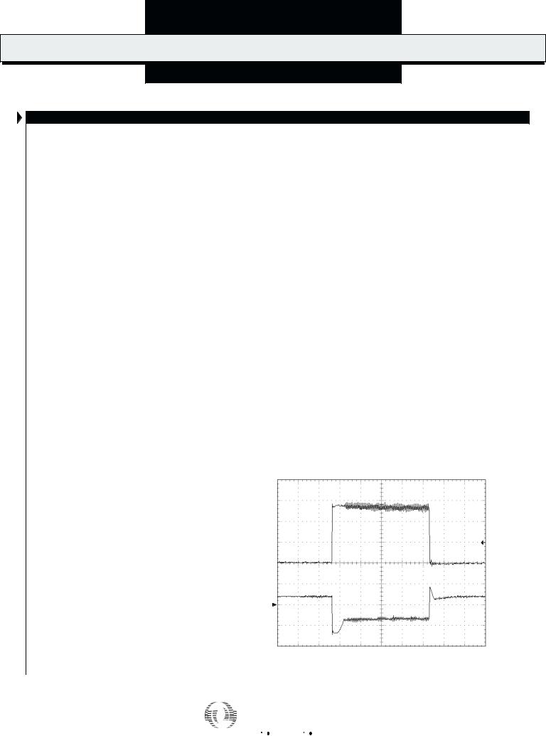
Adaptive Transient Voltage Output
In order to improve transient response a 40mV offset is built into the Current Sense comparator. At high currents, the peak output voltage will be lower than the nominal set point, as shown in Figure 1. The actual output voltage will be a function of the sense resistor, the output current and output ripple.
|
5A/Div. |
|
Output Load 0 to 14A |
||
0A |
|
|
|||
2.8V |
100mV/Div. |
|
|
|
Output Voltage |
|
|
||||
Time - 100µs/Div.
FIGURE 1 — Output Transient Response (using 5mΩ sense resistor and 5µH output inductor)
4 |
|
Copyright © 1999 |
|
Rev. 1.2 11/99 |
|
|
|
|

P R O D U C T D A T A B O O K 1 9 9 6 / 1 9 9 7
LX1664/1664A, LX1665/65A
DUAL OUTPUT PWM CONTROLLERS WITH 5-BIT DAC
P R O D U C T I O N D A T A S H E E T
C H A R A C T E R I S T I C S C U RV E S
|
95 |
|
|
|
|
|
|
|
|
|
|
|
|
|
|
90 |
|
|
|
|
|
|
|
|
|
|
|
|
|
(%) |
85 |
|
|
|
|
|
|
|
|
|
|
|
|
|
EFFICIENCY |
80 |
|
|
|
|
|
|
|
|
|
|
|
|
|
|
|
|
Output Set Point |
|
|
|
|
|
|
|
|
|
||
|
|
|
|
EFFICIENCY AT 3.1V |
|
|
|
|
|
|
|
|
||
|
75 |
|
|
EFFICIENCY AT 2.8V |
|
|
|
|
|
|
|
|
||
|
|
|
|
EFFICIENCY AT 1.8V |
|
|
|
|
|
|
|
|
||
|
70 |
|
|
|
|
|
|
|
|
|
|
|
|
|
|
1 |
2 |
3 |
4 |
5 |
6 |
7 |
8 |
9 |
10 |
11 |
12 |
13 |
14 |
IOUT (A)
FIGURE 2 — Efficiency Test Results:
Non-Synchronous Operation, VIN = 5V
|
100 |
|
|
|
|
|
|
|
|
|
|
|
|
|
|
95 |
|
|
|
|
|
|
|
|
|
|
|
|
|
|
90 |
|
|
|
|
|
|
|
|
|
|
|
|
|
(%) |
|
|
|
|
|
|
|
|
|
|
|
|
|
|
EFFICIENCY |
85 |
|
|
|
|
|
|
|
|
|
|
|
|
|
|
|
|
|
|
|
|
|
|
|
|
|
|
|
|
|
80 |
|
|
|
|
|
|
|
|
|
|
|
|
|
|
|
|
Output Set Point |
|
|
|
|
|
|
|
|
|
||
|
|
|
|
EFFICIENCY AT 3.1V |
|
|
|
|
|
|
|
|
||
|
75 |
|
|
EFFICIENCY AT 2.8V |
|
|
|
|
|
|
|
|
||
|
|
|
EFFICIENCY AT 1.8V |
|
|
|
|
|
|
|
|
|||
|
|
|
|
|
|
|
|
|
|
|
|
|||
|
70 |
|
|
|
|
|
|
|
|
|
|
|
|
|
|
1 |
2 |
3 |
4 |
5 |
6 |
7 |
8 |
9 |
10 |
11 |
12 |
13 |
14 |
IOUT (A)
FIGURE 3 — Efficiency Test Results:
Synchronous Operation, VIN = 5V
90 |
|
|
|
|
|
|
|
|
|
|
|
|
|
85 |
|
|
|
|
|
|
|
|
|
|
|
|
|
80 |
|
|
|
|
|
|
|
|
|
|
|
|
|
75 |
|
|
|
|
|
|
|
|
|
|
|
|
|
70 |
|
|
|
|
|
|
|
|
|
|
|
|
|
|
|
|
|
Output Set Point |
|
|
|
|
|
|
|
|
|
|
|
|
|
|
1.8V EFFICIENCY |
|
|
|
|
|
|
|
|
65 |
|
|
|
|
2.8V EFFICIENCY |
|
|
|
|
|
|
|
|
|
|
|
|
|
3.3V EFFICIENCY |
|
|
|
|
|
|
|
|
60 |
|
|
|
|
|
|
|
|
|
|
|
|
|
1 |
2 |
3 |
4 |
5 |
6 |
7 |
8 |
9 |
10 |
11 |
12 |
13 |
14 |
IOUT (A)
FIGURE 4 — Efficiency Test Results: Synchronous Operation, VIN = 12V.
Note: Non-synchronous operation not recommended for 12V operation, due to power loss in Schottky diode.
Copyright © 1999 |
5 |
Rev. 1.2 11/99 |
P R O D U C T D A T A B O O K 1 9 9 6 / 1 9 9 7
LX1664/64A, LX1665/65A
DUAL OUTPUT PWM CONTROLLERS WITH 5-BIT DAC
|
|
P R O D U C T I O N D A T A S H E E T |
|
|
|
|
|||
|
|
|
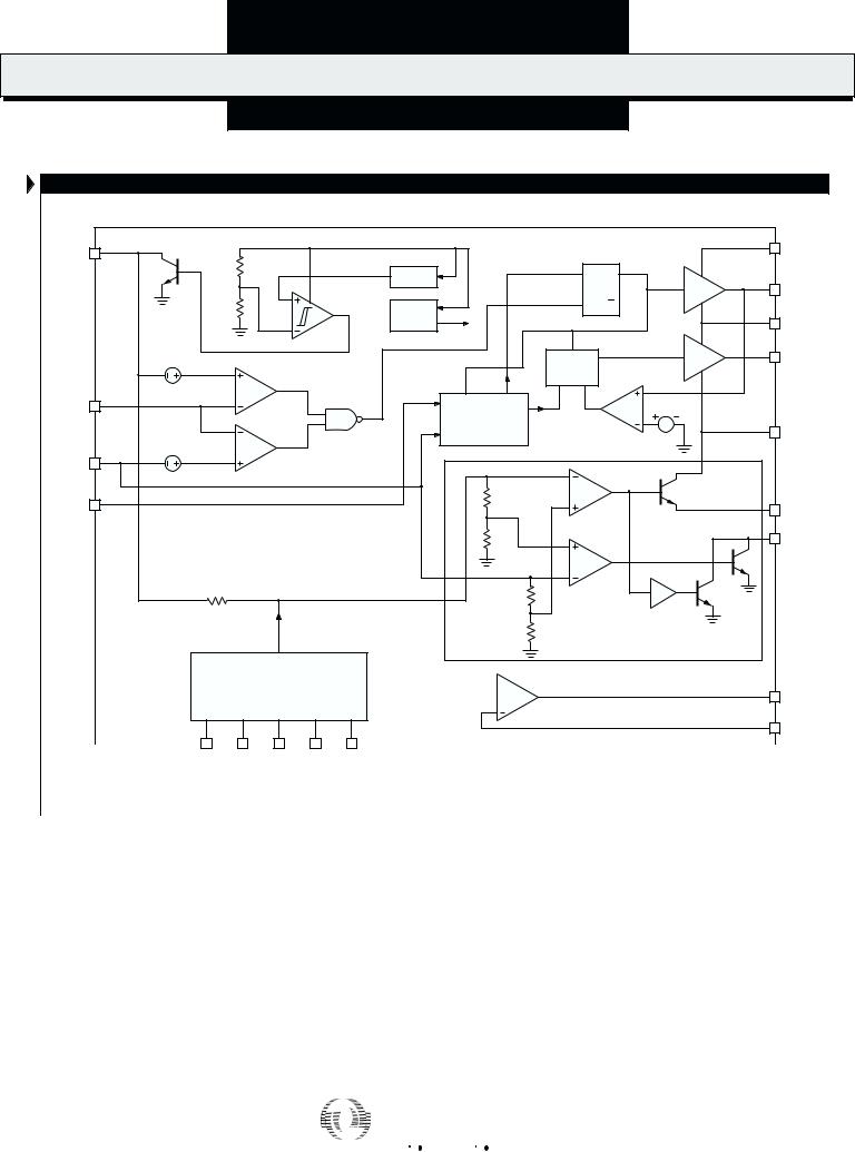
B L O C K D I A G R A M |
|
|
|
|
|
|
|
|
VCC |
|
|
|
|
|
18 |
VC1 |
SS |
1 |
|
|
|
|
PWM Latch |
|||
|
Trimmed |
|
|
|
|
||||
|
|
|
|
|
|
|
|
|
|
|
|
|
2V Out |
|
|
S |
Q |
|
|
|
|
|
2V REF |
|
|
|
|
||
|
|
|
UVLO |
|
R DOM |
|
|
17 |
TDRV |
|
|
|
10.6/10.1 |
|
R |
Q |
|
|
|
|
|
|
Internal |
|
|
|
|
||
|
|
|
|
|
|
|
|
|
|
|
|
|
VCC |
VREG |
|
|
|
16 |
GND |
|
|
|
|
|
|
|
|
|
|
|
|
40mV |
|
|
Break |
|
15 |
BDRV |
|
|
|
|
|
Before |
|
|
|
||
|
|
|
|
|
|
|
|
||
|
|
|
|
|
Make |
|
|
|
|
INV |
2 |
Error Comp |
|
Off-Time |
|
|
|
0.7V |
|
|
|
|
SYNC EN |
|
|||||
|
|
|
|
Controller |
14 |
VCC |
|||
|
|
|
|
|
|
Comp |
|||
VCC_CORE |
3 |
100mV ** |
|
|
|
|
|
|
|
CS Comp |
|
|
|
OV Comp |
|
|
|||
|
|
|
|
|
|
|
|||
CT |
13 |
|
|
|
|
|
|
12 |
OV* |
|
|
|
|
|
|
UV Comp |
10 |
PWRGD* |
|
|
|
10k |
|
|
|
|
|
|
|
|
|
DAC OUT |
|
|
|
|
|
|
|
|
|
|
|
|
|
|
|
LX1665/1665A ONLY |
|
DAC |
1.5V |
|
|
|
|
Linear Op Amp |
|
|
|
|
|
||
|
|
|
|
|
|
11 LDRV
9 LFB
|
4 |
|
|
5 |
|
|
6 |
|
|
7 |
|
|
8 |
|
|
|
|
|
|
|
|
|
|
|
|
|
Note: Pin numbers are correct for LX1665/1665A, 18-pin package. |
||||||
VID0 |
VID1 |
VID2 |
VID3 |
VID4 |
||||||||||||
* Not connected on LX1664/1664A. |
||||||||||||||||
|
|
|
|
|
|
|
|
|
|
|
|
|
|
|
||
** 60mV in LX1664A/1665A.
FIGURE 5 — LX1664/1665 Block Diagram
6 |
|
Copyright © 1999 |
|
Rev. 1.2 11/99 |
|
|
|
|
 Loading...