


 Loading...
8 Bit Microcontroller
TLCS-870/C Series
TMP86FH47BUG

© 2011 TOSHIBA CORPORATION
All Rights Reserved
TMP86FH47BUG
Difference among product (TMP86xx46 Series)
|
86C846 |
86CH46 |
86CM46 |
86PH46 |
|
86PM46 |
|
86FH46 |
|
86FH46A |
|
86CH46A |
86CM46A |
|
86PM46A |
|
|
86FH46B |
|||
|
|
|
|
|
|
|
||||
ROM |
8192bytes |
16384bytes |
32768bytes |
16384bytes |
|
32768bytes |
|
|
16384bytes |
|
(MASK) |
(MASK) |
(MASK) |
(OTP) |
|
(OTP) |
|
|
(FLASH) |
||
|
|
|
|
|||||||
RAM |
512bytes |
512bytes |
1024bytes |
512bytes |
|
1024bytes |
|
512bytes |
|
512bytes |
|
|
|
|
|
|
|
|
|
|
|
|
|
|
|
|
|
|
|
|
|
128bytes (Flash con- |
DBR(note1) |
|
|
|
- |
|
|
|
|
|
trol register con- |
|
|
|
|
|
|
|
|
|
|
tained) |
I/O |
|
|
|
|
33pins |
|
|
|
||
|
|
|
|
|
|
|
|
|
||
Large current out- |
|
|
|
|
19pins |
|
|
|
||
put |
|
|
|
(LED direct drive) |
|
|
|
|||
Interrupt |
|
|
|
18interrupt sources |
|
|
|
|||
|
|
|
(External : 6 Internal : 12) |
|
|
|
||||
|
|
|
|
|
|
|
||||
Timer counter |
|
|
|
16-bit timer counter : 1ch |
|
|
|
|||
|
|
|
8-bit timer counter : 2ch |
|
|
|
||||
|
|
|
|
|
|
|
||||
UART |
|
|
|
8-bit UART : 1ch |
|
|
|
|||
|
|
|
|
|
|
|
|
|||
SIO |
|
|
|
High-Speed SIO : 1ch |
|
|
|
|||
|
|
|
|
|
|
|
|
|
|
|
Key-on wakeup |
|
|
|
|
|
4ch |
|
|
|
|
|
|
|
|
|
|
|
|
|
|
|
10-bit AD convert- |
|
|
|
Analog-input : 8ch |
|
|
|
|||
er |
|
|
|
|
|
|
||||
|
|
|
|
|
|
|
|
|
|
|
|
|
|
|
|
86FH46A |
|
|
||
|
|
|
|
|
|
VDD |
|
|
|
|
|
|
|
|
R |
|
|
|
|
|
|
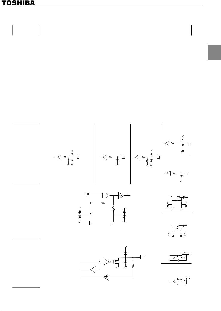
without protect diode |
VDD |
without pull |
|
|
|
||
Structure |
VDD |
down resister |
|
|
|
||||
|
on the VDD side |
|
|
|
|
||||
|
|
|
|
|
|
|
|
||
|
|
|
|
|
|
|
|
|
|
of TEST pin |
R |
|
R |
R |
86FH46B |
|
|
||
|
|
|
|
|
|
||||
|
RIN |
|
|
R |
|
|
|
|
|
|
|
without pull |
IN |
|
|
|
|
|
|
|
|
|
|
|
|
|
|
||
|
|
down resister |
|
without protect diode |
|||||
|
|
|
|
|
|||||
|
|
|
|
|
on the VDD side |
||||
|
|
|
|
|
R |
|
|
|
|
|
|
|
|
|
without pull |
|
|
|
|
|
|
|
|
|
down resister |
|
|
|
|
|
|
|
|
|
86FH46A |
|
|
||
|
|
|
XTEN |
|
|
|
|
|
|
|
Osc. enable |
|
fs |
|
|
XTEN |
|
|
|
|
|
|
|
|
|
|
|
||
|
|
|
|
Osc. enable |
|
|
|
|
|
|
|
|
|
|
|
|
|
fs |
|
|
|
|
|
|
|
|
|
|
|
|
|
|
|
|
VDD |
Rf |
|
|
VDD |
|
|
|
|
|
|
|
RO |
|
|
|
|
|
|
|
|
|
|
|
|
|
VDD |
Rf |
VDD |
|
|
|
|
|
|
|
|
RO |
|
|
|
|
|
|
|
Structure |
|
|
|
XTIN |
XTOUT |
|
|||
|
|
|
|
|
|
|
|
|
|
of XTIN,XTOUT |
|
|
|
|
86FH46B |
|
|
||
|
|
|
|
|
|
|
|||
|
|
|
|
|
|
XTEN |
|
|
|
|
|
|
|
|
Osc. enable |
|
|
|
fs |
|
|
|
|
|
|
|
|
|
|
|
XTIN |
|
XTOUT |
|
|
|
|
|
|
|
|
|
|
|
|
Rf |
RO |
|
|
|
|
|
|
|
|
|
|
||
|
|
|
|
|
XTIN |
XTOUT |
|
||
|
|
|
|
|
86FH46A |
|
|
||
|
|
|
|
|
|
|
|
|
|
|
|
|
|
|
|
|
|
||
|
|
|
|
|
|
|
|
|
|
|
|
|
|
|
|
|
|
|
|
|
|
|
|
|
|
|
|
|
|
|
|
|
|
|
|
|
|
|
|
Structure |
|
|
|
|
|
|
|
|
|
|
|
|
|
|
|
|
|
||
of P2 port |
|
|
|
|
86FH46B |
|
|
||
|
|
|
|
|
|
|
|
|
|
|
|
|
|
|
Initial "High-Z" |
|
|
|
|
|
|
|
|
|
Data output |
|
|
|
|
|
|
|
|
|
|
|
|
|
|
|
|
|
|
|
Input from |
|
|
|
R |
|
|
|
|
|
|
|
|
|
|
|
|
|
|
|
output latch |
|
|
|
|
|
|
|
|
|
Pin input |
|
|
|
|

TMP86FH47BUG
|
86C846 |
86CH46 |
86CM46 |
86PH46 |
|
86PM46 |
86FH46 |
86FH46A |
|
86CH46A |
86CM46A |
|
86PM46A |
86FH46B |
|||
|
|
|
|
|
||||
Number of guaran- |
|
|
|
|
|
|
|
(a)86FH46A |
|
|
|
|
|
|
|
100 Times |
|
teed writes to |
|
- |
|
|
- |
100 Times |
||
|
|
|
(b)86FH46B |
|||||
flash memory |
|
|
|
|
|
|
|
|
|
|
|
|
|
|
|
1000 Times |
|
|
|
|
|
|
|
|
|
|
Terminal for SERI- |
|
|
|
|
|
|
BOOT1/RXD(P10) |
BOOT/RXD(P02) |
AL PROM MODE |
|
|
- |
|
|
|
||
|
|
|
|
|
BOOT2/TXD(P11) |
TXD(P03) |
||
(note2) |
|
|
|
|
|
|
||
|
|
|
|
|
|
|
|
|
|
|
|
|
|
|
|
|
(a)86FH46A |
|
|
|
|
|
|
|
|
Read protect |
Flash Security |
|
|
N.A. |
|
|
|
Read protect |
(b)86FH46B |
|
|
|
|
|
|
|
|
Read / Write |
|
|
|
|
|
|
|
|
protect |
Emulation Chip |
|
|
|
TMP86C947XB |
|
|
||
|
|
|
|
|
|
|
||
Package |
|
|
|
SDIP42-P-600-1.78 |
|
|
||
Note 1: The products with Flash memory (86FH46,86FH46A,86FH46B) contain the Flash control register (FLSCR) at 0FFFH in the DBR area. The products with mask ROM or OTP and the emulation chip do not have the FLSCR register. In these devices,therefore, a program that accesses the FLSCR register cannot function properly (executes differently as in the case of a Flash product).
Note 2: The TXD and RXD pins to be used in Serial PROM mode differ between the 86FH46 and the 86FH46A,86FH46B. Take this into consideration in your board design when you replace the product. Details of the function refer to the chapter of the 86FH46,86FH46A,86FH46B data sheet.
Note 3: P21,P22 combine XTIN,XTOUT and port.
TMP86FH47BUG
Difference among product (TMP86xx47 Series)
|
86C847 |
86CH47 |
86CM47 |
86PH47 |
|
86PM47 |
|
86FH47 |
|
86FH47A |
|
86CH47A |
86CM47A |
|
86PM47A |
|
|
86FH47B |
|||
|
|
|
|
|
|
|
||||
ROM |
8192bytes |
16384bytes |
32768bytes |
16384bytes |
|
32768bytes |
|
|
16384bytes |
|
(MASK) |
(MASK) |
(MASK) |
(OTP) |
|
(OTP) |
|
|
(FLASH) |
||
|
|
|
|
|||||||
RAM |
512bytes |
512bytes |
1024bytes |
512bytes |
|
1024bytes |
|
512bytes |
|
512bytes |
|
|
|
|
|
|
|
|
|
|
|
|
|
|
|
|
|
|
|
|
|
128bytes (Flash con- |
DBR(note1) |
|
|
|
- |
|
|
|
|
|
trol register con- |
|
|
|
|
|
|
|
|
|
|
tained) |
I/O |
|
|
|
|
35pins |
|
|
|
||
|
|
|
|
|
|
|
|
|
||
Large current out- |
|
|
|
|
19pins |
|
|
|
||
put |
|
|
|
(LED direct drive) |
|
|
|
|||
Interrupt |
|
|
|
18interrupt sources |
|
|
|
|||
|
|
|
(External : 6 Internal : 12) |
|
|
|
||||
|
|
|
|
|
|
|
||||
Timer counter |
|
|
|
16-bit timer counter : 1ch |
|
|
|
|||
|
|
|
8-bit timer counter : 2ch |
|
|
|
||||
|
|
|
|
|
|
|
||||
UART |
|
|
|
8-bit UART : 1ch |
|
|
|
|||
|
|
|
|
|
|
|
|
|||
SIO |
|
|
|
High-Speed SIO : 1ch |
|
|
|
|||
|
|
|
|
|
|
|
|
|
|
|
Key-on wakeup |
|
|
|
|
|
4ch |
|
|
|
|
|
|
|
|
|
|
|
|
|
|
|
10-bit AD convert- |
|
|
|
Analog-input : 8ch |
|
|
|
|||
er |
|
|
|
|
|
|
||||
|
|
|
|
|
|
|
|
|
|
|
|
|
|
|
|
|
|
86FH47A |
|
|
||
|
|
|
|
|
|
|
|
VDD |
|
|
|
|
|
|
|
|
|
|
R |
|
|
|
|
|
|
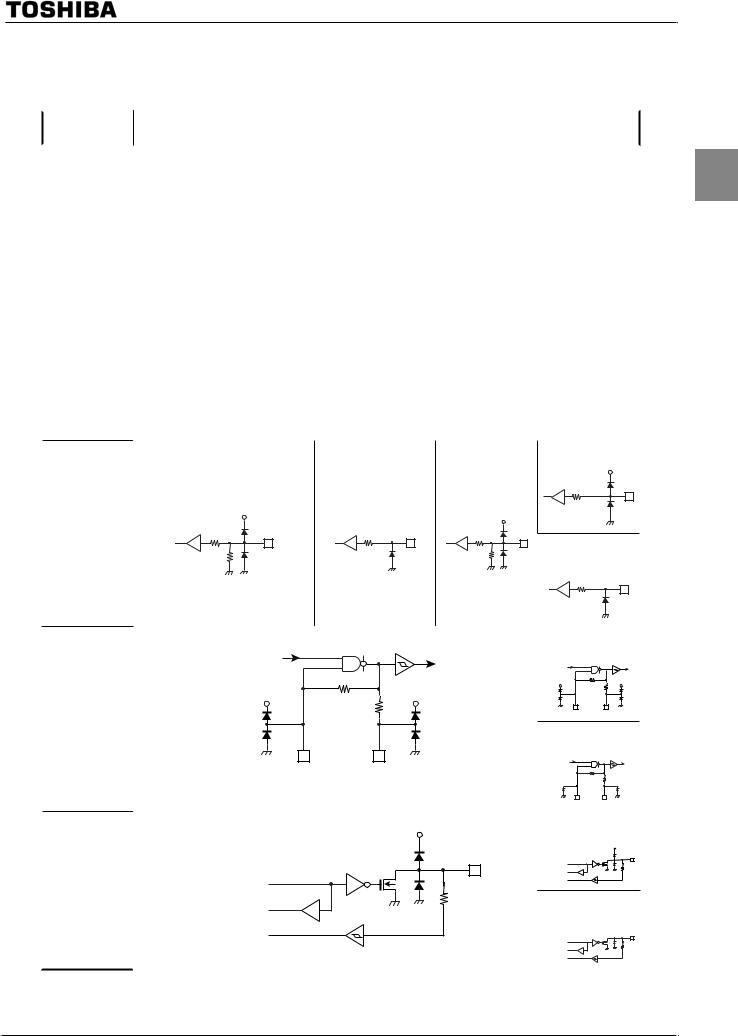
VDD |
without protect diode |
|
without pull |
|
|
|
|||
Structure |
|
VDD |
down resister |
|
|
|
|||||
|
|
|
on the VDD side |
|
|
|
|||||
|
|
|
|
|
|
|
|
|
|
||
R |
|
|
|
|
|
|
|
|
|
|
|
of TEST pin |
|
|
R |
R |
|
86FH47B |
|
|
|||
|
|
|
|
|
|
|
|
||||
|
R |
IN |
without pull |
RIN |
|
|
|
|
|
|
|
|
|
|
|
without protect diode |
|||||||
|
|
|
down resister |
|
|||||||
|
|
|
|
|
on the VDD side |
||||||
|
|
|
|
|
|
|
|||||
|
|
|
|
|
|
|
R |
|
|
|
|
|
|
|
|
|
|
without pull |
|
|
|
||
|
|
|
|
|
|
down resister |
|
|
|
||
|
|
|
|
|
|
|
86FH47A |
|
|
||
|
|
|
|
XTEN |
|
|
|
|
|
|
|
|
|
Osc. enable |
|
|
fs |
|
|
XTEN |
|
|
|
|
|
|
|
|
|
|
|
|
|
||
|
|
|
|
|
Osc. enable |
|
|
|
|
|
|
|
|
|
|
|
|
|
|
|
|
fs |
|
|
|
|
|
|
|
|
|
|
|
|
|
|
|
|
|
|
|
VDD |
|
Rf |
|
|
VDD |
|
|
|
|
|
|
|
|
|
RO |
|
|
|
|
|
|
|
|
|
|
|
|
|
|
|
|
VDD |
Rf |
VDD |
|
|
|
|
|
|
|
|
|
|
RO |
|
|
|
|
|
|
|
|
Structure |
|
|
|
|
|
XTIN |
XTOUT |
|
|||
|
|
|
|
|
|
|
|
|
|
|
|
of XTIN,XTOUT |
|
|
|
|
|
|
86FH47B |
|
|
||
|
|
|
|
|
|
|
|
|
|||
|
|
|
|
|
|
|
|
XTEN |
|
|
|
|
|
|
|
|
|
Osc. enable |
|
|
|
|
fs |
|
|
|
|
|
|
|
|
|
|
|
|
|
|
XTIN |
|
XTOUT |
|
|
|
|
|
|
|
|
|
|
|
|
|
|
|
Rf |
RO |
|
|
|
|
|
|
|
|
|
|
|
|
||
|
|
|
|
|
|
|
XTIN |
XTOUT |
|
||
|
|
|
|
|
|
|
86FH47A |
|
|
||
|
|
|
|
|
|
|
|
|
|
|
|
|
|
|
|
|
|
|
|
|
|
||
|
|
|
|
|
|
|
|
|
|
|
|
|
|
|
|
|
|
|
|
|
|
|
|
|
|
|
|
|
|
|
|
|
|
|
|
|
|
|
|
|
|
|
|
|
|
|
|
Structure |
|
|
|
|
|
|
|
|
|
|
|
|
|
|
|
|
|
|
|
|
|||
of P2 port |
|
|
|
|
|
86FH47B |
|
|
|||
|
|
|
|
|
|
|
|
|
|
|
|
|
|
|
|
|
|
Initial "High-Z" |
|
|
|
|
|
|
|
|
|
|
|
Data output |
|
|
|
|
|
|
|
|
|
|
|
|
|
|
|
|
|
|
|
|
|
|
|
Input from |
|
|
|
|
R |
|
|
|
|
|
|
output latch |
|
|
|
|
|
|
|
|
|
|
|
Pin input |
|
|
|
|
|

TMP86FH47BUG
|
86C847 |
86CH47 |
86CM47 |
86PH47 |
|
86PM47 |
86FH47 |
86FH47A |
|
86CH47A |
86CM47A |
|
86PM47A |
86FH47B |
|||
|
|
|
|
|
||||
Number of guaran- |
|
|
|
|
|
|
|
(a)86FH47A |
|
|
|
|
|
|
|
100 Times |
|
teed writes to |
|
- |
|
|
- |
100 Times |
||
|
|
|
(b)86FH47B |
|||||
flash memory |
|
|
|
|
|
|
|
|
|
|
|
|
|
|
|
1000 Times |
|
|
|
|
|
|
|
|
|
|
Terminal for SERI- |
|
|
|
|
|
|
BOOT1/RXD(P10) |
BOOT/RXD(P02) |
AL PROM MODE |
|
|
- |
|
|
|
||
|
|
|
|
|
BOOT2/TXD(P11) |
TXD(P03) |
||
(note2) |
|
|
|
|
|
|
||
|
|
|
|
|
|
|
|
|
|
|
|
|
|
|
|
|
(a)86FH47A |
|
|
|
|
|
|
|
|
Read protect |
Flash Security |
|
|
N.A. |
|
|
|
Read protect |
(b)86FH47B |
|
|
|
|
|
|
|
|
Read / Write |
|
|
|
|
|
|
|
|
protect |
Emulation Chip |
|
|
|
TMP86C947XB |
|
|
||
|
|
|
|
|
|
|
|
|
Package |
|
Available |
|
|
|
|
|
|
(LQFP44- |
Available |
Available |
N.A. |
|
Available |
Available |
N.A. |
|
(86CH47) |
|
|||||||
P-1010-0.80A) |
|
|
|
|
|
|
|
|
|
|
|
|
|
|
|
|
|
Package |
|
Available |
|
|
|
|
|
|
(LQFP44- |
N.A. |
N.A. |
Available |
|
N.A. |
N.A. |
Available |
|
(86CH47A) |
|
|||||||
P-1010-0.80B) |
|
|
|
|
|
|
|
|
|
|
|
|
|
|
|
|
|
Note 1: The products with Flash memory (86FH47,86FH47A,86FH47B) contain the Flash control register (FLSCR) at 0FFFH in the DBR area. The products with mask ROM or OTP and the emulation chip do not have the FLSCR register. In these devices,therefore, a program that accesses the FLSCR register cannot function properly (executes differently as in the case of a Flash product).
Note 2: The TXD and RXD pins to be used in Serial PROM mode differ between the 86FH47 and the 86FH47A,86FH47B.
Take this into consideration in your board design when you replace the product. Details of the function refer to the chapter of the 86FH47,86FH47A,86FH47B data sheet.
Note 3: P21,P22 combine XTIN,XTOUT and port.

TMP86FH47BUG
Differences in Electrical Characteristics (TMP86xx46 Series)
Read/
Fetch
Operating condition
(MCU
mode)
Erase/
Program
Operating condition
(Serial PROM mode)
Supply voltage
(Absolute Maximum Ratings)
Operating current
86C846 / 86CH46 / 86CM46 |
|
|
|
|
|
86PH46 |
|
|
|
|
|
|
|
|
|
|
|
|
|
|
|
|
|
|
86FH46A |
|
|
|
||||||||||||||||
|
|
|
|
86CM46A |
|
|
|
|
|
|
|
|
|
|
86FH46 |
|
|
|
|
|
|
|
|
|
|
|
|
|||||||||||||||||
|
|
|
|
|
|
|
|
86CH46A |
|
|
|
|
|
|
|
|
|
|
|
|
|
|
86FH46B |
|
|
|
||||||||||||||||||
|
|
|
|
86PM46 |
|
|
|
|
|
|
|
|
|
|
|
|
|
|
|
|
|
|
|
|
|
|
|
|
|
|||||||||||||||
|
|
|
|
|
|
|
|
|
|
|
|
|
|
|
|
|
|
|
|
|
|
|
|
|
|
|
|
|
|
|
|
|
|
|
|
|
|
|||||||
[V] |
|
|
|
|
|
|
|
|
|
[V] |
|
|
|
|
|
|
|
|
|
[V] |
|
|
|
|
|
|
|
|
|
|
|
|
[V] |
|
|
|
|
|
|
|
|
|
||
5.5 |
|
|
|
|
|
|
|
|
|
5.5 |
|
|
|
|
|
|
|
|
|
5.5 |
|
|
|
|
|
|
|
|
|
|
|
|
5.5 |
|
|
|
|
|
|
|
|
|
|
|
4.5 |
|
|
|
|
|
|
|
|
|
4.5 |
|
|
|
|
|
|
|
|
|
4.5 |
|
|
|
|
|
|
|
|
|
|
|
(a) |
4.5 |
|
|
|
|
|
|
|
|
|
(a) |
|
|
|
|
|
|
|
|
|
|
|
|
|
|
|
|
|
|
|
|
|
|
|
|
|
|
|
|
|
|
|
|
|
|
|
|
|
|
|
|
|
|
|
|
||
|
|
|
|
|
|
|
|
|
|
|
|
|
|
|
|
|
|
|
(a) |
|
|
|
|
|
|
|
|
|
|
|
|
|
|
|
|
|
|
|
|
|
|
|
|
|
|
|
|
|
|
|
|
|
|
(a) |
|
|
|
|
|
|
|
|
|
|
|
|
|
|
|
|
|
|
|
|
|
|
|
|
|
|
|
|
|
|
|
|
|
|
|
|
|
|
|
|
|
|
|
|
|
|
|
|
|
|
|
|
|
|
|
|
|
|
|
|
|
|
|
|
|
|
|
|
3.0 |
|
|
|
|
|
|
|
|
|
(b) |
|
|
|
|
|
|
|
|
|
|
|
|
|
|
|
|
|
|
|
|
|
|
|
|
|
|
|
|
|
|
|
|
|
|
|
|
|
|
|
|
|
|
|
|
||
2.7 |
|
|
|
|
|
|
|
|
|
2.7 |
|
|
|
|
|
|
|
|
|
2.7 |
|
|
|
|
|
|
|
|
|
|
|
|
2.7 |
|
|
|
|
|
|
|
|
(Note2) |
||
|
|
|
|
|
|
|
|
|
|
2.0 |
|
|
|
|
|
|
|
|
|
|
|
|
|
|
|
|
|
|
|
|
|
|
|
|
|
|
|
|
|
|
|
|||
|
|
|
|
|
|
|
|
|
|
|
|
|
|
|
|
|
|
|
(b) |
|
|
|
|
|
|
|
|
|
|
|
|
|
|
|
|
|
|
|
|
|
|
|
|
|
1.8 |
|
|
|
|
|
|
|
|
|
1.8 |
|
|
|
|
|
|
|
(Note1) |
1.8 |
|
|
|
|
|
|
|
|
|
|
|
|
1.8 |
|
|
|
|
|
|
|
|
|
|
||
|
|
|
|
|
|
|
|
|
|
|
|
|
|
|
|
|
|
|
|
|
|
|
|
|
|
|
|
|
|
|
|
|
|
|
|
|
|
|
|
|
|
|||
|
|
|
|
|
|
|
|
|
|
|
|
|
|
|
|
|
|
|
|
|
|
|
|
|
|
|
|
|
|
|
|
|
|
|
|
|
|
|
|
|
|
|
|
|
| <![if ! IE]> <![endif]>0.030 |
<![if ! IE]> <![endif]>0.034 |
1 4.2 8 16 [MHz] |
<![if ! IE]> <![endif]>0.030 |
<![if ! IE]> <![endif]>0.034 |
1 4.2 8 16 [MHz] |
<![if ! IE]> <![endif]>0.030 |
<![if ! IE]> <![endif]>0.034 |
1 |
4.2 |
8 |
16 |
[MHz] |
<![if ! IE]> <![endif]>0.030 |
<![if ! IE]> <![endif]>0.034 |
1 |
4.2 8 |
16 |
[MHz] |
||||||||||||||||||||||||||
|
|
|
|
|
|
|
|
|
|
|
|
|
|
|
|
|
|
|
|
|
|
|
|
|
|
|
|
|
|
|
|
|
|
|
|
|
|
|
|
|
|
|
||
|
|
|
|
|
|
|
|
|
|
|
|
|
|
|
|
|
|
|
|
|
|
|
|
|
|
|
|
|
|
|
|
|
|
|
|
|
TMP86FH46A |
|
|
|
||||
(a) 1.8V to 5.5V (-40 to 85 °C) |
(a) 2.0V to 5.5V (-40 to 85 °C) |
(a) 2.7V to 5.5V (-40 to 85 °C) |
(a) 3.0V to 5.5V (-40 to 85 °C) |
|||||||||||||||||||||||||||||||||||||||||
(b) 2.7V to 3.0V (-20 to 85 °C) |
||||||||||||||||||||||||||||||||||||||||||||
|
|
|
|
|
|
|
|
|
|
(b) 1.8V to 2.0V (-20 to 85 °C) |
|
|
|
|
|
|
|
|
|
|
|
|
|
|||||||||||||||||||||
|
|
|
|
|
|
|
|
|
|
|
|
|
|
|
|
|
|
|
|
|
|
|
|
|
|
|
TMP86FH46B |
|
|
|
||||||||||||||
|
|
|
|
|
|
|
|
|
|
|
|
|
|
|
|
|
|
|
|
|
|
|
|
|
|
|
|
|
|
|
|
|
|
|
|
|
|
|
|
|||||
|
|
|
|
|
|
|
|
|
|
|
|
|
|
|
|
|
|
|
|
|
|
|
|
|
|
|
|
|
|
|
|
|
(a) 2.7V to 5.5V (-40 to 85 °C) |
|||||||||||
|
|
|
|
|
|
|
|
|
|
|
|
|
|
|
|
|
|
|
|
|
|
|
|
|
|
|
|
|
|
|
|
|
[V] |
|
|
|
|
|
|
|
|
|
||
|
|
|
|
|
|
|
|
|
|
|
|
|
|
|
|
|
|
|
|
|
|
|
|
|
|
|
|
|
|
|
|
|
5.5 |
|
|
|
|
|
|
|
|
|
(a) |
|
|
|
|
|
|
|
|
|
|
|
|
|
|
|
|
|
|
|
|
|
|
|
|
|
|
|
|
|
|
|
|
|
|
|
|
|
|
|
|
|
|
|
|
||
|
|
|
|
- |
|
|
|
|
|
|
|
- |
|
|
|
|
|
|
|
|
- |
|
|
|
|
|
|
4.5 |
|
|
|
|
|
|
|
|
|
|
||||||
|
|
|
|
|
|
|
|
|
|
|
|
|
|
|
|
|
|
|
|
|
|
|
|
|
|
|
|
|
|
|
|
|
|
|
||||||||||
|
|
|
|
|
|
|
|
|
|
|
|
|
|
|
|
|
|
|
|
|
|
|
|
|
2.7 |
|
|
|
|
|
|
|
|
|
|
|||||||||
|
|
|
|
|
|
|
|
|
|
|
|
|
|
|
|
|
|
|
|
|
|
|
|
|
|
|
|
|
|
|
|
|
1.8 |
|
|
|
|
|
|
|
|
|
|
|
|
|
|
|
|
|
|
|
|
|
|
|
|
|
|
|
|
|
|
|
|
|
|
|
|
|
|
|
|
|
|
|
|
|
|
|
|
|
|
|
|
|
|||
|
|
|
|
|
|
|
|
|
|
|
|
|
|
|
|
|
|
|
|
|
|
|
|
|
|
|
|
|
|
|
|
|
<![if ! IE]> <![endif]>0.030 |
<![if ! IE]> <![endif]>0.034 |
1 |
4.2 8 |
16 |
[MHz] |
||||||
|
|
|
|
|
|
|
|
|
|
|
|
|
|
|
|
|
|
|
|
|
|
|
|
|
|
|
|
|
|
|
|
|
|
|
|
|||||||||
|
|
|
|
|
|
|
|
|
|
|
|
|
|
|
|
|
|
|
|
|
|
|
|
|
|
|
|
|
|
|
|
|
(a) 4.5V to 5.5V (-10 to 40 °C) |
|||||||||||
|
|
|
|
|
|
|
|
|
|
|
|
|
|
|
|
|
|
|
|
[V] |
|
|
|
|
|
|
|
|
|
|
|
|
[V] |
|
|
|
|
|
|
|
|
|
||
|
|
|
|
|
|
|
|
|
|
|
|
|
|
|
|
|
|
|
|
5.5 |
|
|
|
|
|
|
|
|
|
|
|
(a) |
5.5 |
|
|
|
|
|
|
|
|
|
(a) |
|
|
|
|
|
|
|
|
|
|
|
|
|
|
|
|
|
|
|
|
|
|
|
|
|
|
|
|
|
|
|
|
|
|
|
|
|
|
|
|
|
|
|
|||
|
|
|
|
- |
|
|
|
|
|
|
|
- |
|
|
|
4.5 |
|
|
|
|
|
|
|
|
|
|
|
|
4.5 |
|
|
|
|
|
|
|
|
|
|
|||||
|
|
|
|
|
|
|
|
|
|
|
|
|
|
|
|
|
|
|
|
|
|
|
|
|
|
|
|
|
|
|
|
|
|
|
|
|||||||||
|
|
|
|
|
|
|
|
|
|
|
|
|
|
2.7 |
|
|
|
|
|
|
|
|
|
|
|
|
2.7 |
|
|
|
|
|
|
|
|
|
|
|||||||
|
|
|
|
|
|
|
|
|
|
|
|
|
|
|
|
|
|
|
|
1.8 |
|
|
|
|
|
|
|
|
|
|
|
|
1.8 |
|
|
|
|
|
|
|
|
|
|
|
|
|
|
|
|
|
|
|
|
|
|
|
|
|
|
|
|
|
|
|
|
|
|
|
|
|
|
|
|
|
|
|
|
|
|
|
|
|
|
|
|
||||
|
|
|
|
|
|
|
|
|
|
|
|
|
|
|
|
|
|
|
|
<![if ! IE]> <![endif]>0.030 |
<![if ! IE]> <![endif]>0.034 |
2 |
4 |
8 |
16 |
[MHz] |
<![if ! IE]> <![endif]>0.030 |
<![if ! IE]> <![endif]>0.034 |
2 |
4.2 8 |
16 |
[MHz] |
||||||||||||
|
|
|
|
|
|
|
|
|
|
|
|
|
|
|
|
|
|
|
|
|
|
|
|
|||||||||||||||||||||
|
|
|
|
|
|
|
|
|
|
|
|
|
|
|
|
|
|
|
|
(a) 4.5V to 5.5V (20 to 30 °C) |
(a) 4.5V to 5.5V (-10 to 40 °C) |
|||||||||||||||||||||||
|
|
|
|
|
|
|
|
|
|
|
|
|
|
|
|
|
|
|
|
|
|
|
|
|
|
|
|
|
|
|
|
|
|
|
|
|
|
86FH46A |
|
|
|
|||
|
|
|
|
|
|
|
|
|
|
|
|
|
|
−0.3 ~ 6.5 |
|
|
|
|
|
|
|
|
|
|
|
|
|
|
|
|
|
|
(a)−0.3 ~ 6.5 |
|
|
|
||||||||
|
|
|
|
|
|
|
|
|
|
|
|
|
|
|
|
|
|
|
|
|
|
|
|
|
|
|
|
|
|
|
|
86FH46B |
|
|
|
|||||||||
|
|
|
|
|
|
|
|
|
|
|
|
|
|
|
|
|
|
|
|
|
|
|
|
|
|
|
|
|
|
|
|
|
|
|
|
|
|
|
|
|
||||
|
|
|
|
|
|
|
|
|
|
|
|
|
|
|
|
|
|
|
|
|
|
|
|
|
|
|
|
|
|
|
|
|
|
|
|
|
|
(a)−0.3 ~ 6.0 |
|
|
|
|||
|
|
|
|
|
|
|
|
|
|
|
|
|
|
|
|
|
|
|
|
|
|
|
|
|
|
|
|
|
|
|
|
|
|
|
|
|
|
|
|
|
|
|
|
|
Operating current varies with each product. For details, refer to the datacheet (electrical chracteristics) of each product.(Note4)
(Note3)
Note 1: With The 86CH46A,PH46 the operating temperature (Topr) is -20 °C to 85 °C when the supply voltage VDD is less than 2.0V.
Note 2: With The 86FH46A, the operating temperature (Topr) is -20 °C to 85 °C when the supply voltage VDD is less than 3.0V.
Note 3: With The 86FH46A,86FH46B when a program is executing in the Flash memory or when data is being read from the
Flash memory, the Flash memory operates in an intermittent manner causing peak currents in the Flash memory momentarily, as shown in Figure. in this case, the supply current IDD(in NORMAL1,NORMAL2 and SLOW1 mode) is defined as the sum of the average peak current and MCU current.
Note 4: About the measurement condition of supply current, VIN level of TEST pin is deffrent between 86FH46B and the other 86xx46 series MCUs. The supply current is defined as follows; VIN of TEST pin: VIN ≤ 0.1V(86FH46B), VIN ≤ 0.2V(others) It is described in the section "Electrical characteristics" of TMP86FH46B in detail.

TMP86FH47BUG
1 machine cycle (4/fc or 4/fs)
Program counter (PC) |
n |
n+1 |
n+2 |
n+3 |
|
|
|
|
|
Momentary Flash current |
|
IDDP-P |
|
|
|
|
|
[mA] |
|
|
|
|
|
|
|
|
|
Max. current |
Sum of average momentary |
|
|
|
|
Typ. current |
Flash current and MCU current |
|
|
|
|
MCU current |
|
Intermittent Operation of Flash Memory

TMP86FH47BUG
Differences in Electrical Characteristics (TMP86xx47 Series)
Read/
Fetch
Operating condition
(MCU
mode)
Erase/
Program
Operating condition
(Serial PROM mode)
Supply voltage
(Absolute Maximum Ratings)
Operating current
86C847 / 86CH47 / 86CM47 |
|
|
|
|
|
86PH47 |
|
|
|
|
|
|
|
|
|
|
|
|
|
86FH47A |
|
|
|
|||||||||||||||
|
|
|
|
86CM47A |
|
|
|
|
|
|
|
|
|
|
86FH47 |
|
|
|
|
|
|
|
||||||||||||||||
|
|
|
|
|
|
|
|
86CH47A |
|
|
|
|
|
|
|
|
|
86FH47B |
|
|
|
|||||||||||||||||
|
|
|
|
86PM47 |
|
|
|
|
|
|
|
|
|
|
|
|
|
|
|
|
|
|
|
|
||||||||||||||
|
|
|
|
|
|
|
|
|
|
|
|
|
|
|
|
|
|
|
|
|
|
|
|
|
|
|
|
|
|
|
|
|
||||||
[V] |
|
|
|
|
|
|
|
|
|
[V] |
|
|
|
|
|
|
|
|
|
[V] |
|
|
|
|
|
|
|
|
[V] |
|
|
|
|
|
|
|
|
|
5.5 |
|
|
|
|
|
|
|
|
|
5.5 |
|
|
|
|
|
|
|
|
|
5.5 |
|
|
|
|
|
|
|
|
5.5 |
|
|
|
|
|
|
|
|
|
4.5 |
|
|
|
|
|
|
|
|
|
4.5 |
|
|
|
|
|
|
|
|
|
4.5 |
|
|
|
|
|
|
|
(a) |
4.5 |
|
|
|
|
|
|
|
|
(a) |
|
|
|
|
|
|
|
|
|
|
|
|
|
|
|
|
|
|
|
|
|
|
|
|
|
|
|
|
|
|
|
|
|
|
|
|
|
|
|
|
|
|
|
|
|
|
|
|
|
|
|
|
|
|
|
|
|
|
(a) |
|
|
|
|
|
|
|
|
|
|
|
|
|
|
|
|
|
|
|
|
|
|
|
|
|
|
|
|
(a) |
|
|
|
|
|
|
|
|
|
|
|
|
|
|
|
|
|
|
|
|
|
|
|
|
|
|
|
|
|
|
|
|
|
|
|
|
|
|
|
|
|
|
|
|
|
|
|
|
|
|
|
|
|
|
|
|
|
|
3.0 |
|
|
|
|
|
|
|
|
(b) |
|
|
|
|
|
|
|
|
|
|
|
|
|
|
|
|
|
|
|
|
|
|
|
|
|
|
|
|
|
|
|
|
|
|
|
|
|
|
|
2.7 |
|
|
|
|
|
|
|
|
|
2.7 |
|
|
|
|
|
|
|
|
|
2.7 |
|
|
|
|
|
|
|
|
2.7 |
|
|
|
|
|
|
|
(Note2) |
|
|
|
|
|
|
|
|
|
|
|
2.0 |
|
|
|
|
|
|
|
|
|
|
|
|
|
|
|
|
|
|
|
|
|
|
|
|
|
|
||
|
|
|
|
|
|
|
|
|
|
|
|
|
|
|
|
|
|
|
(b) |
|
|
|
|
|
|
|
|
|
|
|
|
|
|
|
|
|
|
|
1.8 |
|
|
|
|
|
|
|
|
|
1.8 |
|
|
|
|
|
|
|
(Note1) |
1.8 |
|
|
|
|
|
|
|
|
1.8 |
|
|
|
|
|
|
|
|
|
|
|
|
|
|
|
|
|
|
|
|
|
|
|
|
|
|
|
|
|
|
|
|
|
|
|
|
|
|
|
|
|
|
|
|
|
|
|
||
|
|
|
|
|
|
|
|
|
|
|
|
|
|
|
|
|
|
|
|
|
|
|
|
|
|
|
|
|
|
|
|
|
|
|
|
|
|
|
| <![if ! IE]> <![endif]>0.030 |
<![if ! IE]> <![endif]>0.034 |
1 4.2 8 16 [MHz] |
<![if ! IE]> <![endif]>0.030 |
<![if ! IE]> <![endif]>0.034 |
1 4.2 8 16 [MHz] |
<![if ! IE]> <![endif]>0.030 |
<![if ! IE]> <![endif]>0.034 |
1 4.2 8 16 [MHz] |
<![if ! IE]> <![endif]>0.030 |
<![if ! IE]> <![endif]>0.034 |
1 4.2 8 |
16 [MHz] |
||||||||||||||||||||||||||
86FH47A
(a) 2.0V to 5.5V (-40 to 85 °C)
(a) 3.0V to 5.5V (-40 to 85 °C)
(a) 1.8V to 5.5V (-40 to 85 °C) (a) 2.7V to 5.5V (-40 to 85 °C) (b) 2.7V to 3.0V (-20 to 85 °C)
(b) 1.8V to 2.0V (-20 to 85 °C)
86FH47B
(a) 2.7V to 5.5V (-40 to 85 °C)
[V]
5.5
(a)
4.5
- |
- |
|
|
|
- |
|
|
|
2.7 |
|
|
|
|
|
|
|
|
|
|
||
|
|
|
|
|
|
|
|
|
|
|
1.8 |
|
|
|
|
|
|
|
|
|
|
|
|
|
|
|
|
|
|
|
|
|
|
|
|
|
|
|
|
|
|
|
|
|
|
|
|
|
|
|
|
|
|
|
<![if ! IE]> <![endif]>0.030 |
<![if ! IE]> <![endif]>0.034 |
1 |
4.2 |
8 |
16 |
[MHz] |
||||
|
|
|
|
|
|
|
|
|
|
|
|
|
|
|
|
||||||
|
|
|
|
|
|
|
|
|
|
|
(a) 4.5V to 5.5V (-10 to 40 °C) |
||||||||||
|
|
[V] |
|
|
|
|
|
|
|
|
[V] |
|
|
|
|
|
|
|
|
|
|
|
|
5.5 |
|
|
|
|
|
|
|
(a) |
5.5 |
|
|
|
|
|
|
|
|
|
(a) |
|
|
|
|
|
|
|
|
|
|
|
|
|
|
|
|
|
|
|
|
||
- |
- |
4.5 |
|
|
|
|
|
|
|
|
4.5 |
|
|
|
|
|
|
|
|
|
|
|
|
|
|
|
|
|
|
|
|
|
|
|
|
|
|
|
|
||||
2.7 |
|
|
|
|
|
|
|
|
2.7 |
|
|
|
|
|
|
|
|
|
|
||
|
|
1.8 |
|
|
|
|
|
|
|
|
1.8 |
|
|
|
|
|
|
|
|
|
|
|
|
|
|
|
|
|
|
|
|
|
|
|
|
|
|
|
|
|
|
|
|
|
|
<![if ! IE]> <![endif]>0.030 |
<![if ! IE]> <![endif]>0.034 |
2 4 8 16 [MHz] |
<![if ! IE]> <![endif]>0.030 |
<![if ! IE]> <![endif]>0.034 |
2 |
4.2 |
8 |
16 |
[MHz] |
||||||||||
|
|
|
|
|
|
|
|
||||||||||||||
|
|
(a) 4.5V to 5.5V (20 to 30 °C) |
(a) 4.5V to 5.5V (-10 to 40 °C) |
||||||||||||||||||
|
|
|
|
|
|
|
|
|
|
|
|
|
|
|
86FH47A |
|
|
|
|
||
|
−0.3 ~ 6.5 |
|
|
|
|
|
|
|
|
|
|
|
|
|
(a)−0.3 ~ 6.5 |
|
|
|
|
||
|
|
|
|
|
|
|
|
|
|
|
|
|
|
86FH47B |
|
|
|
|
|||
|
|
|
|
|
|
|
|
|
|
|
|
|
|
|
|
|
|
|
|||
|
|
|
|
|
|
|
|
|
|
|
|
|
|
|
(a)−0.3 ~ 6.0 |
|
|
|
|
||
|
|
|
|
|
|
|
|
|
|
|
|
|
|
|
|
|
|
|
|
|
|
Operating current varies with each product. For details, refer to the datacheet (electrical chracteristics) of each product.(Note4)
(Note3)
Note 1: With The 86CH47A, PH47 the operating temperature (Topr) is -20 °C to 85 °C when the supply voltage VDD is less than 2.0V.
Note 2: With The 86FH47A, the operating temperature (Topr) is -20 °C to 85 °C when the supply voltage VDD is less than 3.0V.
Note 3: With The 86FH47A,86FH47B when a program is executing in the Flash memory or when data is being read from the
Flash memory, the Flash memory operates in an intermittent manner causing peak currents in the Flash memory momentarily, as shown in Figure. in this case, the supply current IDD(in NORMAL1,NORMAL2 and SLOW1 mode) is defined as the sum of the average peak current and MCU current.
Note 4: About the measurement condition of supply current, VIN level of TEST pin is deffrent between 86FH47B and the other 86xx47 series MCUs. The supply current is defined as follows; VIN of TEST pin: VIN ≤ 0.1V(86FH47B), VIN ≤ 0.2V(others) It is described in the section "Electrical characteristics" of TMP86FH47B in detail.

TMP86FH47BUG
1 machine cycle (4/fc or 4/fs)
Program counter (PC) |
n |
n+1 |
n+2 |
n+3 |
|
|
|
|
|
Momentary Flash current |
|
IDDP-P |
|
|
|
|
|
[mA] |
|
|
|
|
|
|
|
|
|
Max. current |
Sum of average momentary |
|
|
|
|
Typ. current |
Flash current and MCU current |
|
|
|
|
MCU current |
|
Intermittent Operation of Flash Memory
Revision History
Date |
Revision |
Comment |
|
|
|
2010/7/23 |
Tentative 1 |
1st Release of Tentative |
|
|
|
2010/10/6 |
1 |
First Release |
|
|
|
2011/5/10 |
2 |
Contents Revised |
|
|
|

Table of Contents
Difference among product (TMP86xx46 Series)
TMP86FH47BUG
1.1 |
Features...................................................................................................................................... |
1 |
1.2 |
Pin Assignment.......................................................................................................................... |
3 |
1.3 |
Block Diagram........................................................................................................................... |
4 |
1.4 |
Pin Names and Functions.......................................................................................................... |
5 |
2. Operational Description
2.1 |
CPU Core Functions ................................................................................................................ |
7 |
|
2.1.1 |
Memory Address Map ....................................................................................................................................................... |
7 |
|
2.1.2 |
Program Memory (Flash) ................................................................................................................................................... |
7 |
|
2.1.3 |
Data Memory (RAM) ......................................................................................................................................................... |
7 |
|
2.2 |
System Clock Controller .......................................................................................................... |
8 |
|
2.2.1 |
Clock Generator ................................................................................................................................................................. |
8 |
|
2.2.2 |
Timing Generator ............................................................................................................................................................. |
10 |
|
2.2.2.1Configuration of timing generator
2.2.2.2Machine cycle
2.2.3 |
Operation Mode Control Circuit ...................................................................................................................................... |
11 |
|
2.2.3.1 Single-clock mode |
|
||
2.2.3.2 |
Dual-clock mode |
|
|
2.2.3.3 |
STOP mode |
|
|
2.2.4 |
Operating Mode Control .................................................................................................................................................. |
16 |
|
2.2.4.1STOP mode
2.2.4.2IDLE1/2 mode and SLEEP1/2 mode
2.2.4.3IDLE0 and SLEEP0 modes (IDLE0, SLEEP0)
2.2.4.4SLOW mode
2.3 Reset Circuit ........................................................................................................................... |
29 |
|
2.3.1 |
External Reset Input ......................................................................................................................................................... |
29 |
2.3.2 |
Address trap reset ............................................................................................................................................................. |
30 |
2.3.3 |
Watchdog timer reset ....................................................................................................................................................... |
30 |
2.3.4 |
System clock reset ............................................................................................................................................................ |
30 |
3. Interrupt Control Circuit
3.1 |
Interrupt latches (IL15 to IL2) ............................................................................................... |
31 |
3.2 |
Interrupt enable register (EIR) ............................................................................................... |
32 |
3.2.1 Interrupt master enable flag (IMF) .................................................................................................................................. |
32 |
|
3.2.2 Individual interrupt enable flags (EF15 to EF4) ............................................................................................................. |
32 |
|
3.3 |
Interrupt Source Selector (INTSEL)....................................................................................... |
35 |
3.4 |
Interrupt Sequence ................................................................................................................ |
35 |
3.4.1 Interrupt acceptance processing is packaged as follows. ................................................................................................ |
35 |
|
3.4.2 Saving/restoring general-purpose registers ...................................................................................................................... |
36 |
|
3.4.2.1Using PUSH and POP instructions
3.4.2.2Using data transfer instructions
3.4.3 |
Interrupt return ................................................................................................................................................................. |
38 |
i

|
|
|
|
|
|
|
|
|
|
|
|
|
|
|
|
|
|
|
|
|
|
|
|
|
|
|
|
|
|
|
|
|
|
|
|
|
|
|
|
|
|
|
|
|
|
|
|
|
|
|
|
|
|
3.5 |
..................................................................................................Software Interrupt (INTSW) |
39 |
||||||
3.5.1 |
Address error detection .................................................................................................................................................... |
39 |
||||||
3.5.2 |
Debugging ........................................................................................................................................................................ |
39 |
||||||
3.6 |
Undefined Instruction Interrupt (INTUNDEF) ...................................................................... |
39 |
||||||
3.7 |
Address Trap Interrupt (INTATRAP) ................................................................................... |
39 |
||||||
3.8 |
External Interrupts .................................................................................................................. |
39 |
||||||
4. Special Function Register (SFR)
4.1 |
SFR.......................................................................................................................................... |
43 |
4.2 |
DBR......................................................................................................................................... |
45 |
5. Time Base Timer (TBT)
|
5.1 |
Time Base Timer..................................................................................................................... |
47 |
|
|
5.1.1 |
Configuration..................................................................................................................................................................... |
47 |
|
|
5.1.2 |
Control............................................................................................................................................................................... |
47 |
|
|
5.1.3 |
Function............................................................................................................................................................................. |
48 |
|
|
5.2 |
Divider Output (DVO)............................................................................................................ |
49 |
|
|
5.2.1 |
Configuration..................................................................................................................................................................... |
49 |
|
|
5.2.2 |
Control............................................................................................................................................................................... |
49 |
|
|
|
|
||
|
|
|
||
6. |
Watchdog Timer (WDT) |
|
||
|
6.1 |
Watchdog Timer Configuration ............................................................................................. |
51 |
|
|
6.2 |
Watchdog Timer Control ....................................................................................................... |
52 |
|
|
6.2.1 Malfunction Detection Methods Using the Watchdog Timer ......................................................................................... |
52 |
||
|
6.2.2 |
Watchdog Timer Enable .................................................................................................................................................. |
53 |
|
|
6.2.3 |
Watchdog Timer Disable ................................................................................................................................................. |
54 |
|
|
6.2.4 Watchdog Timer Interrupt (INTWDT) ............................................................................................................................ |
54 |
||
|
6.2.5 |
Watchdog Timer Reset ..................................................................................................................................................... |
55 |
|
|
6.3 |
Address Trap .......................................................................................................................... |
56 |
|
|
6.3.1 Selection of Address Trap in Internal RAM (ATAS) ..................................................................................................... |
56 |
||
|
6.3.2 Selection of Operation at Address Trap (ATOUT) ......................................................................................................... |
56 |
||
|
6.3.3 Address Trap Interrupt (INTATRAP)............................................................................................................................... |
56 |
||
|
6.3.4 |
Address Trap Reset........................................................................................................................................................... |
57 |
|
|
|
|
||
|
|
|
||
7. |
I/O Ports |
|
||
|
7.1 |
Port P0 (P07 to P00)............................................................................................................... |
60 |
|
|
7.2 |
Port P1 (P17 to P10)............................................................................................................... |
61 |
|
|
7.3 |
Port P2 (P22 to P20)............................................................................................................... |
62 |
|
|
7.4 |
Port P3 (P37 to P30)............................................................................................................... |
63 |
|
|
7.5 |
Port P4 (P47 to P40)............................................................................................................... |
65 |
|
|
|
|||
|
|
|||
8. 16-Bit Timer/Counter 1 (TC1) |
|
|||
|
8.1 |
Configuration........................................................................................................................... |
67 |
|
|
8.2 |
Timer/Counter Control............................................................................................................ |
68 |
|
ii

|
|
|
|
|
|
|
|
|
|
|
|
|
|
|
|
|
|
|
|
|
|
|
|
|
|
|
|
|
|
|
|
|
|
|
|
|
|
|
|
|
|
|
|
|
|
|
|
|
...................................................................................................................................8.3 Function |
70 |
|||||
8.3.1 |
Timer mode........................................................................................................................................................................ |
70 |
|||||
|
8.3.2 External Trigger Timer Mode........................................................................................................................................... |
72 |
|||||
8.3.3 |
Event Counter Mode......................................................................................................................................................... |
74 |
|||||
8.3.4 |
Window Mode................................................................................................................................................................... |
75 |
|||||
|
8.3.5 Pulse Width Measurement Mode...................................................................................................................................... |
76 |
|||||
|
8.3.6 Programmable Pulse Generate (PPG) Output Mode........................................................................................................ |
79 |
|||||
9. 8-Bit TimerCounter (TC3, TC4)
9.1 |
Configuration .......................................................................................................................... |
83 |
9.2 |
TimerCounter Control............................................................................................................. |
84 |
9.3 |
Function................................................................................................................................... |
89 |
9.3.1 8-Bit Timer Mode (TC3 and 4)........................................................................................................................................ |
89 |
9.3.2 8-Bit Event Counter Mode (TC3, 4)................................................................................................................................. |
90 |
9.3.3 8-Bit Programmable Divider Output (PDO) Mode (TC3, 4)........................................................................................... |
90 |
9.3.4 8-Bit Pulse Width Modulation (PWM) Output Mode (TC3, 4)...................................................................................... |
93 |
9.3.5 16-Bit Timer Mode (TC3 and 4)...................................................................................................................................... |
95 |
9.3.6 16-Bit Event Counter Mode (TC3 and 4)......................................................................................................................... |
96 |
9.3.7 16-Bit Pulse Width Modulation (PWM) Output Mode (TC3 and 4).............................................................................. |
96 |
9.3.8 16-Bit Programmable Pulse Generate (PPG) Output Mode (TC3 and 4)....................................................................... |
99 |
9.3.9 Warm-Up Counter Mode................................................................................................................................................. |
101 |
9.3.9.1Low-Frequency Warm-up Counter Mode
(NORMAL1 → NORMAL2 → SLOW2 → SLOW1)
9.3.9.2High-Frequency Warm-Up Counter Mode
(SLOW1 → SLOW2 → NORMAL2 → NORMAL1)
10. Synchronous Serial Interface (SIO)
10.1 |
Configuration ...................................................................................................................... |
103 |
10.2 |
Control................................................................................................................................. |
104 |
10.3 |
Function............................................................................................................................... |
106 |
10.3.1 |
Serial clock.................................................................................................................................................................... |
106 |
|
10.3.1.1 |
Clock source |
|
|
10.3.1.2 |
Shift edge |
|
|
10.3.2 |
Transfer bit direction..................................................................................................................................................... |
108 |
|
10.3.2.1Transmit mode
10.3.2.2Receive mode
10.3.2.3Transmit/receive mode
10.3.3 Transfer modes.............................................................................................................................................................. |
109 |
10.3.3.1Transmit mode
10.3.3.2Receive mode
10.3.3.3Transmit/receive mode
11.Asynchronous Serial interface (UART)
11.1 |
Configuration ...................................................................................................................... |
121 |
11.2 |
Control ................................................................................................................................ |
122 |
11.3 |
Transfer Data Format.......................................................................................................... |
125 |
11.4 |
Transfer Rate....................................................................................................................... |
126 |
11.5 |
Data Sampling Method........................................................................................................ |
126 |
11.6 |
STOP Bit Length................................................................................................................. |
127 |
11.7 |
Parity.................................................................................................................................... |
127 |
11.8 |
Transmit/Receive Operation................................................................................................ |
127 |
11.8.1 |
Data Transmit Operation............................................................................................................................................... |
127 |
11.8.2 |
Data Receive Operation................................................................................................................................................. |
127 |
iii

|
|
|
|
|
|
|
|
|
|
|
|
|
|
|
|
|
|
|
|
|
|
|
|
|
|
|
|
|
|
|
|
|
|
|
|
|
|
|
|
|
|
|
|
|
|
|
|
11.9 |
...........................................................................................................................Status Flag |
128 |
|||||
11.9.1 |
Parity Error.................................................................................................................................................................... |
128 |
|||||
11.9.2 |
Framing Error................................................................................................................................................................ |
128 |
|||||
11.9.3 |
Overrun Error................................................................................................................................................................ |
128 |
|||||
11.9.4 Receive Data Buffer Full.............................................................................................................................................. |
129 |
||||||
11.9.5 Transmit Data Buffer Empty......................................................................................................................................... |
129 |
||||||
11.9.6 |
Transmit End Flag......................................................................................................................................................... |
130 |
|||||
12. 10-bit AD Converter (ADC)
12.1 |
Configuration ...................................................................................................................... |
131 |
12.2 |
Register configuration......................................................................................................... |
132 |
12.3 |
Function.............................................................................................................................. |
135 |
12.3.1 |
Software Start Mode...................................................................................................................................................... |
135 |
12.3.2 |
Repeat Mode.................................................................................................................................................................. |
135 |
12.3.3 |
Register Setting............................................................................................................................................................ |
136 |
12.4 |
STOP/SLOW Modes during AD Conversion..................................................................... |
137 |
12.5 |
Analog Input Voltage and AD Conversion Result............................................................. |
138 |
12.6 |
Precautions about AD Converter........................................................................................ |
139 |
12.6.1 Analog input pin voltage range..................................................................................................................................... |
139 |
|
12.6.2 Analog input shared pins............................................................................................................................................... |
139 |
|
12.6.3 |
Noise Countermeasure................................................................................................................................................... |
139 |
13. Key-on Wakeup (KWU)
13.1 |
Configuration....................................................................................................................... |
141 |
13.2 |
Control................................................................................................................................. |
141 |
13.3 |
Function............................................................................................................................... |
141 |
14. Flash Memory
14.1 |
|
Flash Memory Control........................................................................................................ |
144 |
14.1.1 Flash Memory Command Sequence Execution Control (FLSCR<FLSMD>)............................................................ |
144 |
||
14.2 |
|
Command Sequence............................................................................................................ |
145 |
14.2.1 |
Byte Program................................................................................................................................................................. |
145 |
|
14.2.2 Sector Erase (4-kbyte Erase)......................................................................................................................................... |
145 |
||
14.2.3 Chip Erase (All Erase).................................................................................................................................................. |
146 |
||
14.2.4 |
Product ID Entry........................................................................................................................................................... |
146 |
|
14.2.5 |
Product ID Exit.............................................................................................................................................................. |
146 |
|
14.2.6 |
Security Program........................................................................................................................................................... |
146 |
|
14.3 |
|
Toggle Bit (D6)................................................................................................................... |
147 |
14.4 |
Access to the Flash Memory Area...................................................................................... |
148 |
|
14.4.1 Flash Memory Control in the Serial PROM Mode...................................................................................................... |
148 |
||
14.4.1.1How to write to the flash memory by executing the control program in the RAM area (in the RAM loader mode within the
serial PROM mode) |
|
14.4.2 Flash Memory Control in the MCU mode................................................................................................................... |
150 |
14.4.2.1How to write to the flash memory by executing a user write control program in the RAM area (in the MCU mode)
15.Serial PROM Mode
15.1 |
Outline................................................................................................................................. |
153 |
15.2 |
Memory Mapping................................................................................................................ |
153 |
15.3 |
Serial PROM Mode Setting................................................................................................ |
154 |
iv

|
|
|
|
|
|
|
|
|
|
|
|
|
|
|
|
|
|
|
|
|
|
|
|
|
|
|
|
|
|
|
|
|
|
|
|
|
|
|
|
|
|
|
|
|
|
|
|
|
.................................................................................................................................15.3.1 Serial PROM Mode Control Pins |
154 |
|||||
|
15.3.2 |
Pin Function................................................................................................................................................................... |
154 |
||||
|
15.3.3 Example Connection for On-Board Writing................................................................................................................. |
155 |
|||||
|
15.3.4 Activating the Serial PROM Mode............................................................................................................................... |
156 |
|||||
|
15.4 |
Interface Specifications for UART..................................................................................... |
157 |
||||
|
15.5 |
Operation Command........................................................................................................... |
158 |
||||
|
15.6 |
Operation Mode................................................................................................................... |
158 |
||||
|
15.6.1 Flash Memory Erasing Mode (Operating command: F0H)......................................................................................... |
160 |
|||||
|
15.6.2 Flash Memory Writing Mode (Operation command: 30H)......................................................................................... |
162 |
|||||
|
15.6.3 RAM Loader Mode (Operation Command: 60H)........................................................................................................ |
165 |
|||||
|
15.6.4 Flash Memory SUM Output Mode (Operation Command: 90H)................................................................................ |
167 |
|||||
|
15.6.5 Product ID Code Output Mode (Operation Command: C0H)..................................................................................... |
168 |
|||||
|
15.6.6 Flash Memory Status Output Mode (Operation Command: C3H).............................................................................. |
170 |
|||||
|
15.6.7 Flash Memory security program Setting Mode (Operation Command: FAH)............................................................ |
172 |
|||||
|
15.7 |
Error Code........................................................................................................................... |
174 |
||||
|
15.8 |
Checksum (SUM)................................................................................................................ |
174 |
||||
|
15.8.1 |
Calculation Method....................................................................................................................................................... |
174 |
||||
|
15.8.2 |
Calculation data............................................................................................................................................................. |
175 |
||||
|
15.9 |
Intel Hex Format (Binary)................................................................................................... |
176 |
||||
|
15.10 |
Passwords.......................................................................................................................... |
176 |
||||
|
15.10.1 Password String........................................................................................................................................................... |
177 |
|||||
|
15.10.2 Handling of Password Error........................................................................................................................................ |
177 |
|||||
|
15.10.3 Password Management during Program Development.............................................................................................. |
177 |
|||||
|
15.11 |
Product ID Code................................................................................................................ |
178 |
||||
|
15.12 Flash Memory Status Code............................................................................................... |
178 |
|||||
|
15.13 |
Specifying the Erasure Area.............................................................................................. |
180 |
||||
|
15.14 Port Input Control Register............................................................................................... |
180 |
|||||
|
15.15 |
Flowchart........................................................................................................................... |
182 |
||||
|
15.16 |
UART Timing................................................................................................................... |
183 |
||||
|
|
|
|
|
|
|
|
|
|
|
|
|
|
|
|
16. |
Input/Output Circuitry |
|
|||||
|
16.1 |
Control Pins......................................................................................................................... |
185 |
||||
|
16.2 |
Input/Output Ports............................................................................................................... |
186 |
||||
|
|
|
|
|
|
|
|
|
|
|
|
|
|
|
|
17. |
Electrical Characteristics |
|
|||||
|
17.1 |
Absolute Maximum Ratings................................................................................................ |
187 |
||||
|
17.2 |
Operating Conditions........................................................................................................... |
188 |
||||
|
17.2.1 |
Serial PROM mode....................................................................................................................................................... |
188 |
||||
|
17.2.2 MCU mode (Except Flash Programming or erasing) ................................................................................................. |
188 |
|||||
|
17.2.3 MCU mode (Flash Programming or erasing) .............................................................................................................. |
189 |
|||||
|
17.3 |
DC Characteristics .............................................................................................................. |
190 |
||||
|
17.4 |
AD Characteristics............................................................................................................... |
192 |
||||
|
17.5 |
AC Characteristics............................................................................................................... |
193 |
||||
|
17.6 |
Flash Characteristics............................................................................................................ |
194 |
||||
|
17.6.1 |
Write Characteristics..................................................................................................................................................... |
194 |
||||
|
17.7 |
Oscillating Conditions......................................................................................................... |
195 |
||||
|
17.8 |
Handling Precaution............................................................................................................ |
195 |
||||
18. Package Dimensions
v

vi

TMP86FH47BUG
CMOS 8-Bit Microcontroller
TMP86FH47BUG
The TMP86FH47BUG is a single-chip 8-bit high-speed and high-functionality microcomputer incorporating 16384 bytes of Flash Memory. It is pin-compatible with the TMP86CH47AUG/TMP86C847UG (Mask ROM version). The TMP86FH47BUG can realize operations equivalent to those of the TMP86CH47AUG/TMP86C847UG by programming the on-chip Flash Memory.
Product No. |
ROM |
RAM |
Package |
MASK ROM MCU |
Emulation Chip |
|
(FLASH) |
||||||
|
|
|
|
|
||
TMP86FH47BUG |
16384 |
512 |
P-LQFP44-1010-0.80B |
TMP86CH47AUG/ |
TMP86C947XB |
|
bytes |
bytes |
TMP86C847UG |
||||
|
|
|
1.1Features
1.8-bit single chip microcomputer TLCS-870/C series
-Instruction execution time :
0.25μs (at 16 MHz)
122 μs (at 32.768 kHz)
-132 types & 731 basic instructions
2.18interrupt sources (External : 6 Internal : 12)
3.Input / Output ports (35 pins)
Large current output: 19pins (Typ. 20mA), LED direct drive
4.Prescaler
-Time base timer
-Divider output function
5.Watchdog Timer
6.16-bit timer counter: 1 ch
-Timer, External trigger, Window, Pulse width measurement,
Event counter, Programmable pulse generate (PPG) modes
7.8-bit timer counter : 2 ch
-Timer, Event counter, Programmable divider output (PDO),
Pulse width modulation (PWM) output, Programmable pulse generation (PPG),
16bit mode (8bit timer 2ch combination) modes
8.Serial Interface
-High-Speed 8-bit SIO: 1ch
9.8-bit UART : 1 ch
This product uses the Super Flash® technology under the licence of Silicon Storage Technology, Inc. Super Flash® is registered trademark of Silicon Storage Technology, Inc.
Page 1
RA000

1.1 Features |
TMP86FH47BUG |
|
10.10-bit successive approximation type AD converter
-Analog input: 8 ch
11.Key-on wakeup : 4 ch
12.Clock operation
Single clock mode
Dual clock mode
13. Low power consumption operation
STOP mode: Oscillation stops. (Battery/Capacitor back-up.)
SLOW1 mode: Low power consumption operation using low-frequency clock.(High-frequency clock stop.)
SLOW2 mode: Low power consumption operation using low-frequency clock.(High-frequency clock oscillate.)
IDLE0 mode: CPU stops, and only the Time-Based-Timer(TBT) on peripherals operate using high frequency clock. Release by falling edge of the source clock which is set by TBTCR<TBTCK>.
IDLE1 mode: CPU stops and peripherals operate using high frequency clock. Release by interruputs (CPU restarts).
IDLE2 mode: CPU stops and peripherals operate using high and low frequency clock. Release by interruputs. (CPU restarts).
SLEEP0 mode: CPU stops, and only the Time-Based-Timer(TBT) on peripherals operate using low frequency clock.Release by falling edge of the source clock which is set by TBTCR<TBTCK>.
SLEEP1 mode: CPU stops, and peripherals operate using low frequency clock. Release by interruput. (CPU restarts).
SLEEP2 mode: CPU stops and peripherals operate using high and low frequency clock. Release by interruput.
14.Wide operation voltage:
4.5V to 5.5 V at 16MHz /32.768 kHz
2.7V to 5.5 V at 8 MHz /32.768 kHz
Page 2
RA000
TMP86FH47BUG
1.2 |
Pin Assignment |
|
|
|
|
|
|
|
|
|
|
|
|
|
|
|
|
|
|
|
|
|
|
|
|
|
|
|
|
|
|
|||
|
|
|
<![if ! IE]> <![endif]>P37 (AIN7/STOP5) |
<![if ! IE]> <![endif]>P36 (AIN6/STOP4) |
<![if ! IE]> <![endif]>P35 (AIN5/STOP3) |
<![if ! IE]> <![endif]>P34 (AIN4/STOP2) |
<![if ! IE]> <![endif]>P33 (AIN3) |
<![if ! IE]> <![endif]>P32 (AIN2) |
<![if ! IE]> <![endif]>P31 (AIN1) |
<![if ! IE]> <![endif]>P30 (AIN0) |
|
<![if ! IE]> <![endif]>P10 (PDO3/PWM3/TC3) |
<![if ! IE]> <![endif]>P11 (INT1) |
<![if ! IE]> <![endif]>P12 (INT2/TC1) |
|
|
|
|||||||||||||||||
|
|
|
|
|
||||||||||||||||||||||||||||||
|
|
|
|
|
||||||||||||||||||||||||||||||
|
VAREF |
|
|
|
|
|
|
|
|
|
|
|
|
|
|
|
|
|
|
|
|
|
|
|
|
|
|
|
|
|
P13 |
( |
|
) |
|
|
|
|
|
|
|
|
|
|
|
|
|
|
|
|
|
|
|
|
|
|
|
|
|
|
|
|
|
|
|
||||
|
|
|
|
|
|
|
|
|
|
|
|
|
|
|
|
|
|
|
|
|
|
|
|
|
|
|
|
|
|
|||||
|
|
|
|
|
|
|
|
|
|
|
|
|
|
|
|
|
|
|
|
|
|
|
|
|
|
|
|
|
DVO |
|||||
|
|
|
|
|
|
|
|
|
|
|
|
|
|
|
|
|
|
|
|
|
|
|
|
|
|
|
||||||||
|
AVDD |
|
|
|
|
|
|
|
|
|
|
|
|
|
|
|
|
|
|
|
|
|
|
|
|
|
|
|
|
P14 |
(PPG) |
|||
|
|
|
|
|
|
|
|
|
|
|
|
|
|
|
|
|
|
|
|
|
|
|
|
|
|
|
||||||||
|
|
|
|
|
|
|
|
|
|
|
|
|
|
|
|
|
|
|
|
|
|
|
|
|
|
|
||||||||
|
AVSS |
|
|
|
|
|
|
|
|
|
|
|
|
|
|
|
|
|
|
|
|
|
|
|
|
|
|
|
|
P15 |
(INT3) |
|||
|
|
|
|
|
|
|
|
|
|
|
|
|
|
|
|
|
|
|
|
|
|
|
|
|
|
|
||||||||
|
|
|
|
|
|
|
|
|
|
|
|
|
|
|
|
|
|
|
|
|
|
|
|
|
|
|
||||||||
|
P40 |
|
|
|
|
|
|
|
|
|
|
|
|
|
|
|
|
|
|
|
|
|
|
|
|
|
|
|
|
P16 |
|
|
|
|
|
|
|
|
|
|
|
|
|
|
|
|
|
|
|
|
|
|
|
|
|
|
|
|
|
|
|
|
|
|
|
|
|||
|
|
|
|
|
|
|
|
|
|
|
|
|
|
|
|
|
|
|
|
|
|
|
|
|
|
|
|
|
|
|||||
|
P41 |
|
|
|
|
|
|
|
|
|
|
|
|
|
|
|
|
|
|
|
|
|
|
|
|
|
|
|
|
P17 |
|
|
|
|
|
|
|
|
|
|
|
|
|
|
|
|
|
|
|
|
|
|
|
|
|
|
|
|
|
|
|
|
|
|
|||||
|
|
|
|
|
|
|
|
|
|
|
|
|
|
|
|
|
|
|
|
|
|
|
|
|
|
|
|
|
|
|||||
|
P42 |
|
|
|
|
|
|
|
|
|
|
|
|
|
|
|
|
|
|
|
|
|
|
|
|
|
|
|
|
P07 |
(INT4) |
|||
|
|
|
|
|
|
|
|
|
|
|
|
|
|
|
|
|
|
|
|
|
|
|
|
|
|
|
||||||||
|
|
|
|
|
|
|
|
|
|
|
|
|
|
|
|
|
|
|
|
|
|
|
|
|
|
|
||||||||
|
P43 |
|
|
|
|
|
|
|
|
|
|
|
|
|
|
|
|
|
|
|
|
|
|
|
|
|
|
|
|
P06 |
(SCK) |
|||
|
|
|
|
|
|
|
|
|
|
|
|
|
|
|
|
|
|
|
|
|
|
|
|
|
|
|||||||||
|
|
|
|
|
|
|
|
|
|
|
|
|
|
|
|
|
|
|
|
|
|
|
|
|
|
|
|
|
||||||
|
|
|
|
|
|
|
|
|
|
|
|
|
|
|
|
|
|
|
|
|
|
|
|
|
|
|
|
|
|
|||||
|
P44 |
|
|
|
|
|
|
|
|
|
|
|
|
|
|
|
|
|
|
|
|
|
|
|
|
|
|
|
|
P05 |
(SI) |
|||
|
|
|
|
|
|
|
|
|
|
|
|
|
|
|
|
|
|
|
|
|
|
|
|
|
|
|||||||||
|
|
|
|
|
|
|
|
|
|
|
|
|
|
|
|
|
|
|
|
|
|
|
|
|
|
|
|
|
||||||
|
|
|
|
|
|
|
|
|
|
|
|
|
|
|
|
|
|
|
|
|
|
|
|
|
|
|
|
|
|
|||||
|
P45 |
|
|
|
|
|
|
|
|
|
|
|
|
|
|
|
|
|
|
|
|
|
|
|
|
|
|
|
|
P04 |
(SO) |
|||
|
|
|
|
|
|
|
|
|
|
|
|
|
|
|
|
|
|
|
|
|
|
|
|
|
|
|||||||||
|
|
|
|
|
|
|
|
|
|
|
|
|
|
|
|
|
|
|
|
|
|
|
|
|
|
|
|
|
||||||
|
|
|
|
|
|
|
|
|
|
|
|
|
|
|
|
|
|
|
|
|
|
|
|
|
|
|
|
|
|
|||||
|
P46 |
|
|
|
|
|
|
|
|
|
|
|
|
|
|
|
|
|
|
|
|
|
|
|
|
|
|
|
|
P03 |
(TXD) |
|||
|
|
|
|
|
|
|
|
|
|
|
|
|
|
|
|
|
|
|
|
|
|
|
|
|
|
|||||||||
|
|
|
|
|
|
|
|
|
|
|
|
|
|
|
|
|
|
|
|
|
|
|
|
|
|
|
|
|
||||||
|
|
|
|
|
|
|
|
|
|
|
|
|
|
|
|
|
|
|
|
|
|
|
|
|
|
|
|
|
|
|||||
|
P47 |
|
|
|
|
|
|
|
|
|
|
|
|
|
|
|
|
|
|
|
|
|
|
|
|
|
|
|
|
P02 |
(RXD/BOOT) |
|||
|
|
|
|
|
|
|
|
|
|
|
|
|
|
|
|
|
|
|
|
|
|
|
|
|
|
|
||||||||
|
|
|
|
|
|
|
|
|
|
|
|
|
|
|
|
|
|
|
|
|
|
|
|
|
|
|
||||||||
|
|
|
|
|
|
|
|
|
|
|
|
|
|
|
|
|
|
|
|
|
|
|
|
|
|
|
|
|
|
|
|
|
|
|
|
|
|
|
|
|
|
|
|
|
|
|
|
|
|
|
|
|
|
|
|
|
|
|
|
|
|
|
|
|
|
|
|
|
|
|
|
|
<![if ! IE]> <![endif]>VSS |
<![if ! IE]> <![endif]>XIN |
<![if ! IE]> <![endif]>XOUT |
<![if ! IE]> <![endif]>TEST |
<![if ! IE]> <![endif]>VDD |
<![if ! IE]> <![endif]>(XTIN) P21 |
<![if ! IE]> <![endif]>(XTOUT) P22 |
|
|
|
<![if ! IE]> <![endif]>(INT0) P00 |
|
<![if ! IE]> <![endif]>(PDO4/PWM4/PPG4/TC4) P01 |
|
|
|
||||||||||||||||
|
|
|
|
<![if ! IE]> <![endif]>RESET |
|
<![if ! IE]> <![endif]>(INT5/STOP) P20 |
|
|
|
|
|
|||||||||||||||||||||||
|
|
|
|
|
|
|
|
|
|
|
|
|
|
|
||||||||||||||||||||
|
|
|
|
|
|
|
|
|
|
|
|
|
|
|
|
|
||||||||||||||||||
|
|
|
|
|
|
|
|
|
|
|
|
|
|
|
|
|
|
|
|
|
|
|||||||||||||
|
|
|
|
|
|
|
|
|
|
|
|
|
|
|
|
|
|
|
|
|
|
|
|
|
||||||||||
|
|
|
|
|
|
|
|
|
|
|
|
|
|
|
|
|
|
|
|
|
|
|
|
|
||||||||||
|
|
|
|
|
|
|
|
|
|
|
|
|
|
|
|
|
|
|
|
|
|
|
|
|
|
|
|
|||||||
|
|
|
|
|
|
|
|
|
|
|
|
|
|
|
|
|
|
|
|
|
|
|
|
|
|
|
|
|
|
|
||||
Figure 1-1 Pin Assignment
Page 3
RA000

1.3 Block Diagram |
TMP86FH47BUG |
|
1.3Block Diagram
Figure 1-2 Block Diagram
Page 4
RA000

TMP86FH47BUG
1.4Pin Names and Functions
The TMP86FH47BUG has MCU mode, parallel PROM mode, and serial PROM mode. Table 1-1 shows the pin functions in MCU mode. The serial PROM mode is explained later in a separate chapter.
Table 1-1 Pin Names and Functions(1/3)
|
|
Pin Name |
Pin Number |
Input/Output |
Functions |
||
|
|
|
|
|
|
|
|
|
P07 |
17 |
IO |
PORT07 |
|||
|
INT4 |
I |
External interrupt 4 input |
||||
|
|
||||||
|
|
|
|
|
|
|
|
|
P06 |
16 |
IO |
PORT06 |
|||
|
|
|
|
|
|
Serial clock input/output |
|
|
SCK |
IO |
|||||
|
|
||||||
|
|
|
|
|
|
|
|
|
P05 |
15 |
IO |
PORT05 |
|||
|
SI |
I |
Serial data input |
||||
|
|
||||||
|
|
|
|
|
|
|
|
|
P04 |
14 |
IO |
PORT04 |
|||
|
SO |
O |
Serial data output |
||||
|
|
||||||
|
|
|
|
|
|
|
|
|
P03 |
13 |
IO |
PORT03 |
|||
|
TXD |
O |
UART data output |
||||
|
|
||||||
|
|
|
|
|
|
|
|
|
P02 |
|
IO |
PORT02 |
|||
|
RXD |
12 |
I |
UART data input |
|||
|
BOOT |
|
I |
Serial PROM mode control input |
|||
|
|
|
|
|
|
|
|
|
P01 |
|
IO |
PORT01 |
|||
|
TC4 |
11 |
I |
TC4 input |
|||
|
|
|
|
|
|
O |
PDO4/PWM4/PPG4 output |
|
PDO4/PWM4/PPG4 |
|
|||||
|
|
|
|
|
|
|
|
|
P00 |
10 |
IO |
PORT00 |
|||
|
|
|
|
|
|
|
|
|
INT0 |
I |
External interrupt 0 input |
||||
|
|
||||||
|
|
|
|
|
|
|
|
|
P17 |
18 |
IO |
PORT17 |
|||
|
|
|
|
|
|
|
|
|
P16 |
19 |
IO |
PORT16 |
|||
|
|
|
|
|
|
|
|
|
P15 |
20 |
IO |
PORT15 |
|||
|
INT3 |
I |
External interrupt 3 input |
||||
|
|
||||||
|
|
|
|
|
|
|
|
|
P14 |
21 |
IO |
PORT14 |
|||
|
|
|
|
|
|
|
|
|
PPG |
O |
PPG output |
||||
|
|
||||||
|
|
|
|
|
|
||
|
P13 |
22 |
IO |
PORT13 |
|||
|
|
|
|
|
|
|
|
|
DVO |
O |
Divider Output |
||||
|
|
||||||
|
|
|
|
|
|
||
|
P12 |
|
IO |
PORT12 |
|||
|
INT2 |
23 |
I |
External interrupt 2 input |
|||
|
TC1 |
|
I |
TC1 input |
|||
|
|
|
|
|
|
||
|
P11 |
24 |
IO |
PORT11 |
|||
|
INT1 |
I |
External interrupt 1 input |
||||
|
|
||||||
|
|
|
|
|
|
||
|
P10 |
|
IO |
PORT10 |
|||
|
|
|
25 |
O |
PDO3/PWM3 output |
||
|
PDO3/PWM3 |
||||||
|
TC3 |
|
I |
TC3 input |
|||
|
|
|
|
|
|
|
|
|
P22 |
|
IO |
PORT22 |
|||
|
7 |
Resonator connecting pins(32.768kHz) for inputting exter- |
|||||
|
XTOUT |
O |
|||||
|
|
nal clock |
|||||
|
|
|
|
|
|
|
|
|
|
|
|
|
|
|
|
|
P21 |
|
IO |
PORT21 |
|||
|
6 |
Resonator connecting pins(32.768kHz) for inputting exter- |
|||||
|
XTIN |
I |
|||||
|
|
nal clock |
|||||
|
|
|
|
|
|
|
|
|
|
|
|
|
|
|
|
Page 5
RA000

1.4 Pin Names and Functions |
TMP86FH47BUG |
|
Table 1-1 Pin Names and Functions(2/3)
|
|
|
|
|
Pin Name |
Pin Number |
Input/Output |
Functions |
|
|
|
|
|
|
|
|
|
|
P20 |
|
IO |
PORT20 |
||||
|
|
|
|
|
|
9 |
I |
STOP mode release signal input |
|
STOP |
|||||||
|
|
|
|
|
|
I |
External interrupt 5 input |
|
|
INT5 |
|
||||||
|
|
|
|
|
|
|
||
|
P37 |
|
IO |
PORT37 |
||||
|
AIN7 |
33 |
I |
Analog Input7 |
||||
|
STOP5 |
|
I |
STOP5 input |
||||
|
|
|
|
|
|
|
||
|
P36 |
|
IO |
PORT36 |
||||
|
AIN6 |
32 |
I |
Analog Input6 |
||||
|
STOP4 |
|
I |
STOP4 input |
||||
|
|
|
|
|
|
|
||
|
P35 |
|
IO |
PORT35 |
||||
|
AIN5 |
31 |
I |
Analog Input5 |
||||
|
STOP3 |
|
I |
STOP3 input |
||||
|
|
|
|
|
|
|
||
|
P34 |
|
IO |
PORT34 |
||||
|
AIN4 |
30 |
I |
Analog Input4 |
||||
|
STOP2 |
|
I |
STOP2 input |
||||
|
|
|
|
|
|
|
||
|
P33 |
29 |
IO |
PORT33 |
||||
|
AIN3 |
I |
Analog Input3 |
|||||
|
|
|||||||
|
|
|
|
|
|
|
||
|
P32 |
28 |
IO |
PORT32 |
||||
|
AIN2 |
I |
Analog Input2 |
|||||
|
|
|||||||
|
|
|
|
|
|
|
||
|
P31 |
27 |
IO |
PORT31 |
||||
|
AIN1 |
I |
Analog Input1 |
|||||
|
|
|||||||
|
|
|
|
|
|
|
||
|
P30 |
26 |
IO |
PORT30 |
||||
|
AIN0 |
I |
Analog Input0 |
|||||
|
|
|||||||
|
|
|
|
|
|
|
||
|
P47 |
44 |
IO |
PORT47 |
||||
|
|
|
|
|
|
|
||
|
P46 |
43 |
IO |
PORT46 |
||||
|
|
|
|
|
|
|
||
|
P45 |
42 |
IO |
PORT45 |
||||
|
|
|
|
|
|
|
||
|
P44 |
41 |
IO |
PORT44 |
||||
|
|
|
|
|
|
|
||
|
P43 |
40 |
IO |
PORT43 |
||||
|
|
|
|
|
|
|
||
|
P42 |
39 |
IO |
PORT42 |
||||
|
|
|
|
|
|
|
||
|
P41 |
38 |
IO |
PORT41 |
||||
|
|
|
|
|
|
|
||
|
P40 |
37 |
IO |
PORT40 |
||||
|
|
|
|
|
|
|
||
|
XIN |
2 |
I |
Resonator connecting pins for high-frequency clock |
||||
|
|
|
|
|
|
|
||
|
XOUT |
3 |
O |
Resonator connecting pins for high-frequency clock |
||||
|
|
|
|
|
|
|
||
|
|
|
|
8 |
IO |
Reset signal |
||
|
RESET |
|||||||
|
|
|
|
|
||||
|
TEST |
4 |
I |
Test pin for out-going test. Normally, be fixed to low. |
||||
|
|
|
|
|
||||
|
VAREF |
34 |
I |
Analog Base Voltage Input Pin for A/D Conversion |
||||
|
|
|
|
|
|
|
|
|
Table 1-1 Pin Names and Functions(3/3)
Pin Name |
Pin Number |
Input/Output |
|
Functions |
|
|
|
|
|
AVDD |
35 |
|
I |
Analog Power Supply |
|
|
|
|
|
AVSS |
36 |
|
I |
Analog Power Supply |
|
|
|
|
|
VDD |
5 |
|
I |
+5V |
|
|
|
|
|
VSS |
1 |
|
I |
0(GND) |
|
|
|
|
|
Page 6
RA000

TMP86FH47BUG
2.Operational Description
2.1CPU Core Functions
The CPU core consists of a CPU, a system clock controller, and an interrupt controller.
This section provides a description of the CPU core, the program memory, the data memory, and the reset circuit.
2.1.1Memory Address Map
The TMP86FH47BUG memory is composed Flash, RAM, DBR(Data buffer register) and SFR(Special function register). They are all mapped in 64-Kbyte address space. Figure 2-1 shows the TMP86FH47BUG memory address map.
0000H
SFR 64 bytes 003FH
0040H
RAM
512 bytes
023FH
0F80H
DBR
128
0FFFH bytes
C000H
Flash
16384 bytes
FFC0H
FFDFH
FFE0H
FFFFH
SFR: Special function register includes: I/O ports
Peripheral control registers Peripheral status registers System control registers Program status word
RAM: Random access memory includes: Data memory
Stack
DBR: Data buffer register includes:
Peripheral control registers
Peripheral status registers
Flash: Program memory
Vector table for vector call instructions (32 bytes)
Vector table for interrupts (32 bytes)
Figure 2-1 Memory Address Map
2.1.2Program Memory (Flash)
The TMP86FH47BUG has a 16384 bytes (Address C000H to FFFFH) of program memory (Flash).
2.1.3Data Memory (RAM)
The TMP86FH47BUG has 512bytes (Address 0040H to 023FH) of internal RAM. The first 192 bytes (0040H to 00FFH) of the internal RAM are located in the direct area; instructions with shorten operations are available against such an area.
Page 7

2. |
Operational Description |
|
|
2.2 |
System Clock Controller |
TMP86FH47BUG |
|
|
|
|
|
|
|
|
|
The data memory contents become unstable when the power supply is turned on; therefore, the data memory should be initialized by an initialization routine.
Example :Clears RAM to “00H”. (TMP86FH47BUG)
|
LD |
HL, 0040H |
; Start address setup |
|
LD |
A, H |
; Initial value (00H) setup |
|
LD |
BC, 01FFH |
|
SRAMCLR: |
LD |
(HL), A |
|
|
INC |
HL |
|
|
DEC |
BC |
|
|
JRS |
F, SRAMCLR |
|
2.2System Clock Controller
The system clock controller consists of a clock generator, a timing generator, and a standby controller.
|
|
|
|
|
|
|
|
|
|
|
|
|
|
|
Timing generator control register |
|
|
|
||||||||||||
|
|
|
|
|
|
|
|
|
|
|
|
|
|
|
|
|
|
|
|
|
|
|
|
|
|
|
|
|
|
|
|
|
|
|
|
|
|
|
|
|
|
|
|
|
|
|
|
|
|
|
TBTCR |
|
|
|
|
|
|
|
|||
|
|
|
|
|
|
|
|
|
|
|
|
Clock |
|
|
|
|
|
|
|
|
|
|
|
|
|
|
|
|||
|
|
|
|
|
|
|
|
|
|
|
|
|
|
|
|
|
|
|
|
0036H |
|
|
|
|
|
|||||
|
|
XIN |
|
|
|
|
|
|
generator |
|
fc |
|
|
|
|
|
|
|
||||||||||||
|
|
|
|
|
|
|
|
|||||||||||||||||||||||
|
|
|
|
|
|
|
|
|
|
|
|
|
|
|
|
|||||||||||||||
|
|
|
|
|
|
|
|
|
|
|
|
|
|
|
|
|
|
|
|
|
|
|||||||||
|
|
|
|
High-frequency |
|
Timing |
|
|
|
Standby controller |
|
|||||||||||||||||||
|
|
|
|
|
|
|
|
|
|
|
|
|
|
|
|
|
|
|
|
|
||||||||||
|
|
|
|
|
|
|
|
|
|
|
|
|
|
|
|
|
|
|
|
|
||||||||||
|
|
|
|
|
|
|
|
|
|
|
clock oscillator |
|
|
|
|
|
|
generator |
|
|
|
|
|
|
|
|||||
|
|
|
|
|
|
|
|
|
|
|
|
|
|
|
|
|
|
|
|
|
|
|
|
|||||||
|
|
XOUT |
|
|
|
|
|
|
|
|
|
|
|
|
|
|
|
|
|
|
|
|
0038H |
0039H |
||||||
|
|
|
|
|
|
|
|
|
|
|
|
|
|
|
|
|
|
|
||||||||||||
|
|
|
|
|
|
|
|
|
|
|
|
|
|
|
|
|
|
|
|
|
||||||||||
|
|
XTIN |
|
|
|
|
|
|
|
|
fs |
|
|
|
|
|
|
|
|
|
|
|
SYSCR1 |
|
SYSCR2 |
|
||||
|
|
|
|
|
|
|
|
|
|
|
Low-frequency |
|
|
|
|
|
System clocks |
|
System control registers |
|||||||||||
|
|
|
|
|
|
|
|
|
|
|
|
|
|
|
|
|
||||||||||||||
|
|
|
|
|
|
|
|
|
|
|
clock oscillator |
|
|
|
|
|
|
|
|
|
|
|||||||||
|
|
|
|
|
|
|
|
|
|
|
|
|
|
|
|
|
|
|
|
|
|
|
|
|
|
|
|
|||
|
|
XTOUT |
|
|
|
|
|
|
|
|
|
|
|
|
|
|
|
|
|
|
|
|
|
|
|
|
|
|||
|
|
|
|
|
|
|
|
|
|
|
|
|
|
|
Clock generator control |
|
|
|
|
|
||||||||||
|
|
|
|
|
|
|
|
|
|
|
|
|
|
|
|
|
|
|
||||||||||||
Figure 2-2 System Clock Control
2.2.1Clock Generator
The clock generator generates the basic clock which provides the system clocks supplied to the CPU core and peripheral hardware. It contains two oscillation circuits: One for the high-frequency clock and one for the low-frequency clock. Power consumption can be reduced by switching of the standby controller to low-pow- er operation based on the low-frequency clock.
The high-frequency (fc) clock and low-frequency (fs) clock can easily be obtained by connecting a resonator between the XIN/XOUT and XTIN/XTOUT pins respectively. Clock input from an external oscillator is also possible. In this case, external clock is applied to XIN/XTIN pin with XOUT/XTOUT pin not connected.
Page 8

|
|
|
|
|
|
|
|
|
|
|
|
|
|
|
|
|
|
|
|
|
|
|
|
|
|
|
|
|
|
|
TMP86FH47BUG |
|
|
|
|
|
|
|
|
|
|
|
|
|
|
|
|
||||||||||||||||
|
|
|
|
|
|
|
High-frequency clock |
|
|
|
|
|
|
Low-frequency clock |
|
||||||||||||||||
|
|
|
|
|
|
|
|
|
|
|
|
|
|
||||||||||||||||||
|
|
XIN |
XOUT |
XIN |
XOUT |
XTIN |
|
XTOUT |
XTIN |
XTOUT |
|||||||||||||||||||||
|
|
|
|
|
|
|
|
|
|
|
|
|
|
|
|
(Open) |
|
|
|
|
|
|
|
|
|
|
|
|
|
|
(Open) |
|
|
|
|
|
|
|
|
|
|
|
|
|
|
|
|
|
|
|
|
|
|
|
|
|
|
|
|
|
|
||
|
|
|
|
|
|
|
|
|
|
|
|
|
|
|
|
|
|
|
|
|
|
|
|
|
|
|
|
|
|
|
|
|
|
|
|
|
|
|
|
|
|
|
|
|
|
|
|
|
|
|
|
|
|
|
|
|
|
|
|
|
|
|
|
|
|
|
|
|
|
|
|
|
|
|
|
|
|
|
|
|
|
|
|
|
|
|
|
|
|
|
|
|
|
|
|
|
|
|
|
|
|
|
|
|
|
|
|
|
|
|
|
|
|
|
|
|
|
|
|
|
|
|
|
|
|
|
|
|
|
|
|
|
|
|
|
|
|
|
|
|
|
|
|
|
|
|
|
|
|
|
|
|
|
|
|
|
|
|
|
|
|
|
|
|
|
|
|
|
|
|
|
|
|
|
|
|
|
|
|
|
|
|
|
|
|
|
|
|
|
|
|
|
|
|
|
|
|
|
|
|
|
|
|
|
|
|
|
|
|
|
|
|
|
|
|
|
|
|
|
|
|
|
|
(a) Crystal/Ceramic |
(b) External oscillator |
(c) Crystal |
(d) External oscillator |
|
|
||
resonator |
|
|
|
Figure 2-3 Examples of Resonator Connection
Note:The function to monitor the basic clock directly at external is not provided for hardware, however, with disabling all interrupts and watchdog timers, the oscillation frequency can be adjusted by monitoring the pulse which the fixed frequency is outputted to the port by the program.
The system to require the adjustment of the oscillation frequency should create the program for the adjustment in advance.
Page 9

2.Operational Description
2.2 System Clock Controller |
TMP86FH47BUG |
|
2.2.2Timing Generator
The timing generator generates the various system clocks supplied to the CPU core and peripheral hardware from the basic clock (fc or fs). The timing generator provides the following functions.
1.Generation of main system clock
2.Generation of divider output (DVO) pulses
3.Generation of source clocks for time base timer
4.Generation of source clocks for watchdog timer
5.Generation of internal source clocks for timer/counters
6.Generation of warm-up clocks for releasing STOP mode
2.2.2.1Configuration of timing generator
The timing generator consists of a 2-stage prescaler, a 21-stage divider, a main system clock generator, and machine cycle counters.
An input clock to the 7th stage of the divider depends on the operating mode, SYSCR2<SYSCK> and TBTCR<DV7CK>, that is shown in Figure 2-4. As reset and STOP mode started/canceled, the prescaler and the divider are cleared to “0”.
|
|
|
Main system clock generator |
fc or fs |
Machine cycle counters |
|
|
||
SYSCK |
|
|
|
|
|
|
|
|
|
DV7CK |
|
|
|
|
|
|
|
|
|
|
|
|
|
|
S |
|
Divider |
|
|
High-frequency |
|
|
fc/4 |
|
A |
|
|
|
|
1 |
2 |
1 2 3 4 5 6 |
Y |
7 8 9 |
10 11 12 13 14 15 16 17 18 19 20 21 |
|
|
||
clock fc |
|
|
|
|
B |
|
|
|
|
Low-frequency |
|
|
|
|
Multi- |
|
S |
|
Multiplexer |
|
|
|
|
plexer |
|
|
|||
clock fs |
|
|
|
|
|
B0 |
|
|
|
|
|
|
|
|
|
|
|
||
|
|
|
|
|
|
|
B1 |
|
|
|
|
|
|
|
|
|
A0 |
Y0 |
Warm-up |
|
|
|
|
|
|
|
A1 |
Y1 |
|
|
|
|
|
|
|
|
|
|
controller |
|
|
|
|
|
|
|
|
|
Watchdog |
|
|
|
|
|
|
|
|
|
timer |
Timer counter, Serial interface, Time-base-timer, divider output, etc. (Peripheral functions)
Figure 2-4 Configuration of Timing Generator
Page 10

TMP86FH47BUG
Timing Generator Control Register
TBTCR |
7 |
6 |
5 |
4 |
|
3 |
|
|
2 |
1 |
0 |
|
|
|
(0036H) |
(DVOEN) |
|
|
(DVOCK) |
DV7CK |
(TBTEN) |
|
|
(TBTCK) |
|
(Initial value: 0000 0000) |
|||
|
|
|
|
|
|
|
|
|
|
|
||||
|
DV7CK |
|
Selection of input to the 7th stage |
|
0: fc/28 |
[Hz] |
|
|
|
R/W |
||||
|
|
of the divider |
|
|
|
1: fs |
|
|
|
|
||||
|
|
|
|
|
|
|
|
|
|
|
||||
Note 1: In single clock mode, do not set DV7CK to “1”.
Note 2: Do not set “1” on DV7CK while the low-frequency clock is not operated stably. Note 3: fc: High-frequency clock [Hz], fs: Low-frequency clock [Hz], *: Don’t care
Note 4: In SLOW1/2 and SLEEP1/2 modes, the DV7CK setting is ineffective, and fs is input to the 7th stage of the divider.
Note 5: When STOP mode is entered from NORMAL1/2 mode, the DV7CK setting is ineffective during the warm-up period after release of STOP mode, and the 6th stage of the divider is input to the 7th stage during this period.
2.2.2.2Machine cycle
Instruction execution and peripheral hardware operation are synchronized with the main system clock.
The minimum instruction execution unit is called an “machine cycle”. There are a total of 10 different types of instructions for the TLCS-870/C Series: Ranging from 1-cycle instructions which require one machine cycle for execution to 10-cycle instructions which require 10 machine cycles for execution. A machine cycle consists of 4 states (S0 to S3), and each state consists of one main system clock.
1/fc or 1/fs [s]
Main system clock
State |
|
|
|
|
|
|
|
|
|
|
|
S0 |
S1 |
S2 |
S3 |
S0 |
S1 |
S2 |
S3 |
|
Machine cycle
Figure 2-5 Machine Cycle
2.2.3Operation Mode Control Circuit
The operation mode control circuit starts and stops the oscillation circuits for the high-frequency and low-fre- quency clocks, and switches the main system clock. There are three operating modes: Single clock mode, dual clock mode and STOP mode. These modes are controlled by the system control registers (SYSCR1 and SYSCR2). Figure 2-6 shows the operating mode transition diagram.
2.2.3.1Single-clock mode
Only the oscillation circuit for the high-frequency clock is used, and P21 (XTIN) and P22 (XTOUT) pins are used as input/output ports. The main-system clock is obtained from the high-frequency clock. In the single-clock mode, the machine cycle time is 4/fc [s].
(1)NORMAL1 mode
In this mode, both the CPU core and on-chip peripherals operate using the high-frequency clock. The TMP86FH47BUG is placed in this mode after reset.
Page 11

2. |
Operational Description |
|
|
2.2 |
System Clock Controller |
TMP86FH47BUG |
|
|
|
|
|
|
|
|
|
(2)IDLE1 mode
In this mode, the internal oscillation circuit remains active. The CPU and the watchdog timer are halted; however on-chip peripherals remain active (Operate using the high-frequency clock).
IDLE1 mode is started by SYSCR2<IDLE> = "1", and IDLE1 mode is released to NORMAL1 mode by an interrupt request from the on-chip peripherals or external interrupt inputs. When the IMF (Interrupt master enable flag) is “1” (Interrupt enable), the execution will resume with the acceptance of the interrupt, and the operation will return to normal after the interrupt service is completed. When the IMF is “0” (Interrupt disable), the execution will resume with the instruction which follows the IDLE1 mode start instruction.
(3)IDLE0 mode
In this mode, all the circuit, except oscillator and the timer-base-timer, stops operation.
This mode is enabled by SYSCR2<TGHALT> = "1".
When IDLE0 mode starts, the CPU stops and the timing generator stops feeding the clock to the peripheral circuits other than TBT. Then, upon detecting the falling edge of the source clock selected with TBTCR<TBTCK>, the timing generator starts feeding the clock to all peripheral circuits.
When returned from IDLE0 mode, the CPU restarts operating, entering NORMAL1 mode back again. IDLE0 mode is entered and returned regardless of how TBTCR<TBTEN> is set. When IMF = “1”, EF6 (TBT interrupt individual enable flag) = “1”, and TBTCR<TBTEN> = “1”, interrupt processing is performed. When IDLE0 mode is entered while TBTCR<TBTEN> = “1”, the INTTBT interrupt latch is set after returning to NORMAL1 mode.
2.2.3.2Dual-clock mode
Both the high-frequency and low-frequency oscillation circuits are used in this mode. P21 (XTIN) and P22 (XTOUT) pins cannot be used as input/output ports. The main system clock is obtained from the highfrequency clock in NORMAL2 and IDLE2 modes, and is obtained from the low-frequency clock in SLOW and SLEEP modes. The machine cycle time is 4/fc [s] in the NORMAL2 and IDLE2 modes, and 4/fs [s] (122 μs at fs = 32.768 kHz) in the SLOW and SLEEP modes.
The TLCS-870/C is placed in the single-clock mode during reset. To use the dual-clock mode, the lowfrequency oscillator should be turned on at the start of a program.
(1)NORMAL2 mode
In this mode, the CPU core operates with the high-frequency clock. On-chip peripherals operate using the high-frequency clock and/or low-frequency clock.
(2)SLOW2 mode
In this mode, the CPU core operates with the low-frequency clock, while both the high-frequency clock and the low-frequency clock are operated. As the SYSCR2<SYSCK> becomes "1", the hardware changes into SLOW2 mode. As the SYSCR2<SYSCK> becomes “0”, the hardware changes into NORMAL2 mode. As the SYSCR2<XEN> becomes “0”, the hardware changes into SLOW1 mode. Do not clear SYSCR2<XTEN> to “0” during SLOW2 mode.
(3)SLOW1 mode
This mode can be used to reduce power-consumption by turning off oscillation of the high-frequen- cy clock. The CPU core and on-chip peripherals operate using the low-frequency clock.
Page 12
Loading...