

Service
SA17S1 /F1N/L1G/N1G/S1G
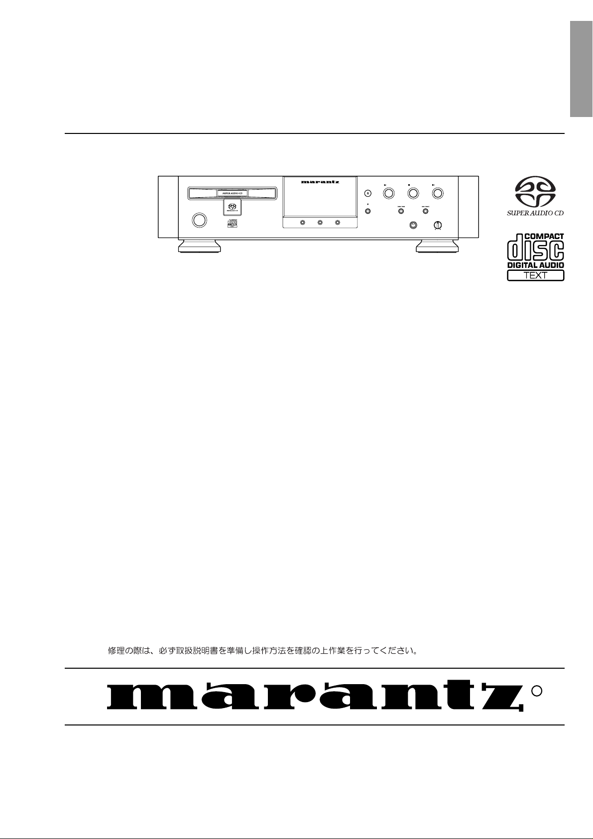
SA-17S1
Manual
POWER
Super Audio CD Player
PHONES
PAUSE
STOP
LEVEL
MIN MAX
PLAY
OPEN/CLOSE
ON/OFF
SUPER AUDIO CD PLAYER SA-17S1
TIME
SOUND MODE
PHANTOM-C
DISPLAY
TABLE OF CONTENTS
SECTION PAGE
1. TECHNICAL SPECIFICATIONS ...................................................................................................1
2. SERVICE MODE...........................................................................................................................2
3. TAKING THE DISC OUT OF EMERGENCY................................................................................. 3
4. CAUTION Optical pick up and Servo Board.................................................................................. 4
5. BLOCK DIAGRAM ........................................................................................................................ 5
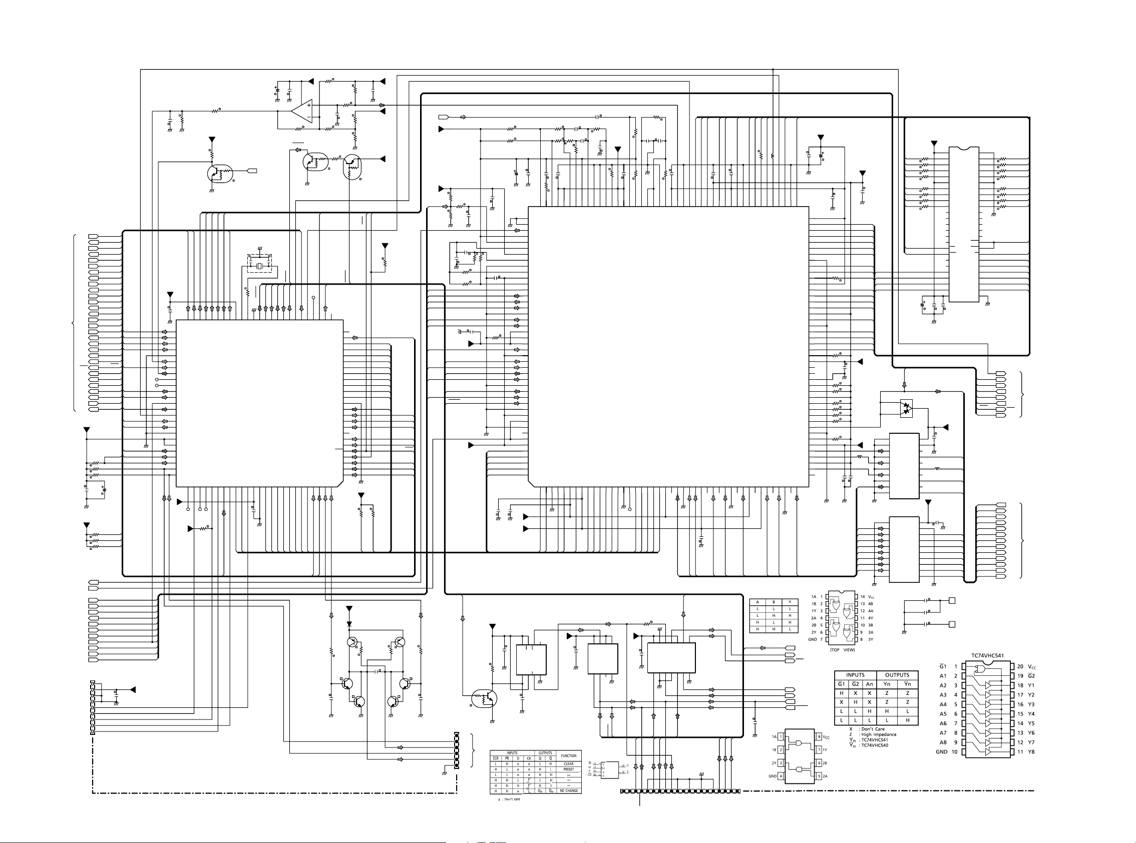
6. SCHEMATIC DIAGRAM................................................................................................................ 7
7. PARTS LOCATION...................................................................................................................... 20
8. MICROPROCESSOR AND IC DATA........................................................................................... 27
9. EXPLODED VIEW AND PARTS LIST......................................................................................... 45
10. MECHA LOADER ASS'Y ............................................................................................................ 48
11. ELECTRICAL PARTS LIST.........................................................................................................49
Please use this service manual with referring to the user guide ( D.F.U. ) without fail.
R
SA-17S1
08AK855010 MIT
First Issue 2002.12
MARANTZ DESIGN AND SERVICE
Using superior design and selected high grade components,
Only original
MARANTZ
parts can insure that your
MARANTZ
MARANTZ
product will continue to perform to the specifi cations for which
company has created the ultimate in stereo sound.
it is famous.
Parts for your
MARANTZ
ORDERING PARTS :
equipment are generally available to our National Marantz Subsidiary or Agent.
Parts can be ordered either by mail or by Fax.. In both cases, the correct part number has to be specifi ed.
The following information must be supplied to eliminate delays in processing your order :
1. Complete address
2. Complete part numbers and quantities required
3. Description of parts
4. Model number for which part is required
5. Way of shipment
6. Signature : any order form or Fax. must be signed, otherwise such part order will be considered as null and void.
USA
MARANTZ AMERICA, INC
1100 MAPLEWOOD DRIVE
ITASCA, IL. 60143
USA
PHONE : 630 - 741 - 0300
FAX : 630 - 741 - 0301
AMERICAS
SUPERSCOPE TECHNOLOGIES, INC.
MARANTZ PROFESSIONAL PRODUCTS
2640 WHITE OAK CIRCLE, SUITE A
AURORA, ILLINOIS 60504 USA
PHONE : 630 - 820 - 4800
FAX : 630 - 820 - 8103
EUROPE / TRADING
MARANTZ EUROPE B.V.
P. O. BOX 8744, BUILDING SILVERPOINT
BEEMDSTRAAT 11, 5653 MA EINDHOVEN
THE NETHERLANDS
PHONE : +31 - 40 - 2507844
FAX : +31 - 40 - 2507860
AUSTRALIA
TECHNICAL AUDIO GROUP PTY, LTD
558 DARLING STREET,
BALMAIN, NSW 2041,
AUSTRALIA
PHONE : 61 - 2 - 9810 - 5300
FAX : 61 - 2 - 9810 - 5355
CANADA
LENBROOK INDUSTRIES LIMITED
633 GRANITE COURT,
PICKERING, ONTARIO L1W 3K1
CANADA
PHONE : 905 - 831 - 6333
FAX : 905 - 831 - 6936
HONG KONG
Jolly ProAudio Broadcast Engineering Ltd.
UNIT 2, 10F, WAH HUNG CENTRE,
41 HUNG TO ROAD, KWUN TONG, KLN.,
HONG KONG
PHONE : 852 - 21913660
FAX : 852 - 21913990
AUSTRALIA
QualiFi Pty Ltd,
24 LIONEL ROAD,
MT. WAVERLEY VIC 3149
AUSTRALIA
PHONE : +61 - (0)3 - 9543 - 1522
FAX : +61 - (0)3 - 9543 - 3677
NEW ZEALAND
WILDASH AUDIO SYSTEMS NZ
14 MALVERN ROAD MT ALBERT
AUCKLAND NEW ZEALAND
PHONE : +64 - 9 - 8451958
FAX : +64 - 9 - 8463554
JAPAN
MARANTZ JAPAN, INC.
35- 1, 7- CHOME, SAGAMIONO
SAGAMIHARA - SHI, KANAGAWA
JAPAN 228-8505
PHONE : +81 42 748 1013
FAX : +81 42 741 9190
Technical
THAILAND
MRZ STANDARD CO., LTD
746 - 754 MAHACHAI ROAD.,
WANGBURAPAPIROM, PHRANAKORN,
BANGKOK, 10200 THAILAND
PHONE : +66 - 2 - 222 9181
FAX : +66 - 2 - 224 6795
TAIWAN
PAI- YUING CO., LTD.
6 TH FL NO, 148 SUNG KIANG ROAD,
TAIPEI, 10429, TAIWAN R.O.C.
PHONE : +886 - 2 - 25221304
FAX : +886 - 2 - 25630415
SHOCK, FIRE HAZARD SERVICE TEST :
SINGAPORE
WO KEE HONG DISTRIBUTION PTE LTD
130 JOO SENG ROAD
#03-02 OLIVINE BUILDING
SINGAPORE 368357
PHONE : +65 6858 5535 / +65 6381 8621
FAX : +65 6858 6078
MALAYSIA
WO KEE HONG ELECTRONICS SDN. BHD.
2ND FLOOR BANGUNAN INFINITE CENTRE
LOT 1, JALAN 13/6, 46200 PETALING JAYA
SELANGOR DARUL EHSAN, MALAYSIA
PHONE : +60 - 3 - 7954 8088
FAX : +60 - 3 - 7954 7088
KOREA
MK ENTERPRISES LTD.
ROOM 604/605, ELECTRO-OFFICETEL, 16-58,
3GA, HANGANG-RO, YONGSAN-KU, SEOUL
KOREA
PHONE : +822 - 3232 - 155
FAX : +822 - 3232 - 154
CAUTION : After servicing this appliance and prior to returning to customer, measure the resistance between either primary AC
cord connector pins ( with unit NOT connected to AC mains and its Power switch ON ), and the face or Front Panel of product
and controls and chassis bottom.
Any resistance measurement less than 1 Megohms should cause unit to be repaired or corrected before AC power is applied,
and verifi ed before it is return to the user/customer.
Ref. UL Standard No. 1492.
In case of diffi culties, do not hesitate to contact the Technical
Department at above mentioned address.
020816MIT

1. TECHNICAL SPECIFICATIONS
Super Audio CD CD
Audio Characteristics
Analog output
Channels 6channels (Max.) 2channels
Frequency range 2Hz — 100kHz 2Hz — 20kHz
Frequency characteristics 2Hz — 50kHz (-3dB) 2Hz — 20kHz
Dynamic range 114dB 100dB
THD (1kHz) 0.0008% 0.0020%
Wow & Flutter Precision of quartz Precision of quartz
Output level 2.2V 2.2V
Digital output
Output level (Cinch JACK) — 0.5Vp-p (75Ω)
Output level (Optical) — -19dBm
Headphone output level 0.5W / 32Ω (max, Vol.) 0.5mW / 32Ω (max, Vol.)
Optical Readout System
Laser AlGaAs AlGaAs
Wave length 650nm 780nm
Signal format 1-bit DSD 16-bit linear PCM
Sampling frequency 2.8224MHz 44.1kHz
Power Supply
Input Voltage, Frequency (/F).................................................................... AC 100V 50/60Hz
(/L)......................................................................... AC 110V 60Hz
(/N/S)..................................................................... AC 230V 50Hz
Power Consumption....................................................................................................... 24W
Cabinet, etc.
Dimensions ...............................................................................................
Net weight...................................................................................................................11.5kg
Operating temperatures.................................................................................. +5°C ~ +35°C
Operating humidity............................................................................. 5 ~ 90% (without dew)
Accessories
• Remote control unit (RC-17SAS1) ....................................................................................1
Dimensions (Width × Height × Depth)....................................................
Net weight (without Batteries) .....................................................................................189g
• AAA (R03) Batteries ..........................................................................................................2
• AC Power cord...................................................................................................................1
• Audio cable...............................................................................................................3 pairs
• Remote connection Cable ................................................................................................1
• User’s Guide......................................................................................................................1
458 × 110 × 394mm
44 × 17.5 × 239mm
1
2. SERVICE MODE
2-1. Factory mode
While pressing <OPEN/CLOSE>and<NEXT>plug in the Mains cord.
Press<
Press<
Press<
Press<
"SA-17S1" is displayed
>
Version of Backend(QF01) u-COM is displayed
"Ver : X.XX" is displayed
>
Version of Frontend(Q125) µ-COM is displayed
"DrvVer : XX.XX" is displayed
>
All parts of FTD is turned on
>
Each Segment is displayed one by one
Press<
Turn off Power to quit Service Mode.
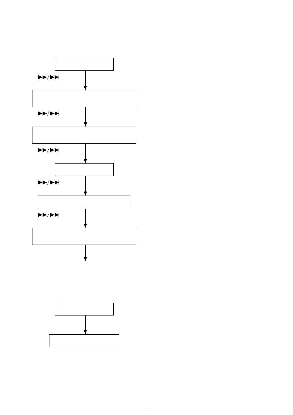
2-2. Reset the unit to the default settings
While pressing <OPEN/CLOSE>and<NEXT>plug in the Mains cord.
Press <PHANTOM-C>
All the setting are restored to the default setting.
When key is depressed,key name is displayed
>
Check of key
"SA-17S1" is displayed
"EEPROM Clear" is displayed
2
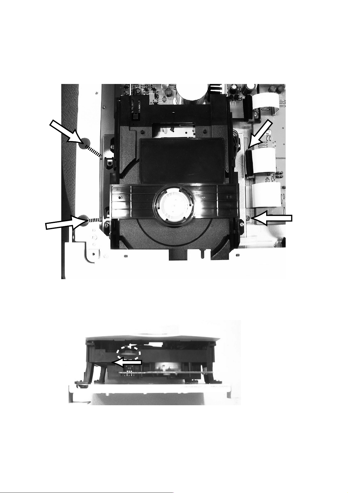
3. TAKING THE DISC OUT OF EMERGENCY
1. Remove 8 screws on the top cover and remove the top cover.
2. Remove 6 screws on the side panel and remove the side panel.
3. Remove Power SW. Link.
4. Remove 4 screws pointed with the arrows.
5. Disconnect all the wires at the right.
6. Remove the Mecha. component.
7. Turn the gear to the direction shown with your fi nger and disc tray will opened.
3
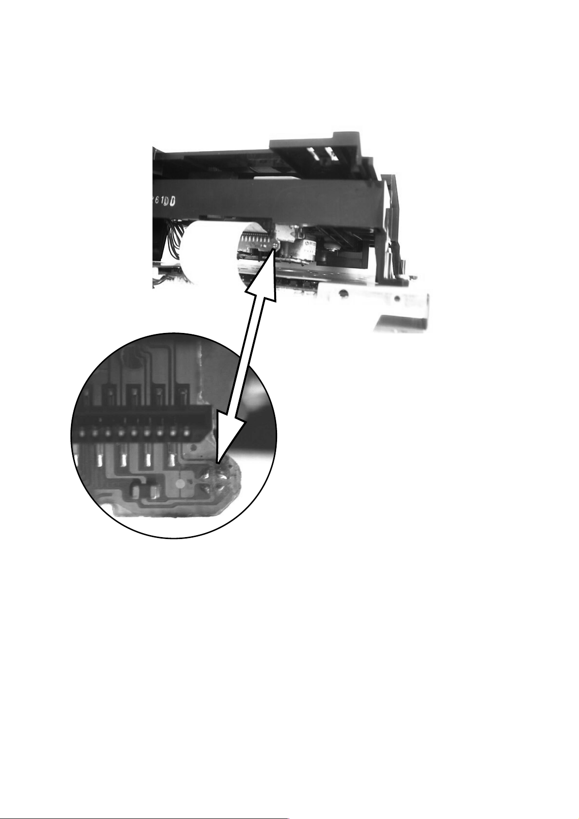
4. CAUTION Optical pick up and Servo Board
When removing the fl at wire between Optical pick up and Servo Board (PV16),
Solder the four lands pointed by arrows to short the circuit.
Otherwise the LASER DIODE may be damaged by static electricity.
4

5. BLOCK DIAGRAM
SACD UNIT BLOCK
TURNTABLE
photo
Laser
control
CD and DVD
FOC,RAD,SLDG
3-AXICAL ACTUATOR
CLV MOTOR
BA5981FP
MOTOR DRIVER
LASER and MONITOR
SERVO SIGNAL
FOC
RAD
M11L1616SA-45
CXD1881R
RF-AMP, AGC, EQ
LASER POWER CONTROL
RF-DC
AMP
CXD3068Q
RF-AC
EFM AMP
33.8688MHz DSARS
RFACO
Control data bus line
CD DECODER
and
D-RAM(16M)
CXD1882R
DSD DECODER
WATER MARK
RF-AMP
SYSTEM CLK SYCL
WARFI
Control data bus line
DIGITAL SERVO
CLV
SLEDG
SERVO CONTOROL MPU
CXP97100
PCM data bus line
MPU data bus line
AT24C04N
EM636165TS-7
LEVEL SHIFT
DIG out
SDRAM(16M)
CXD2752R/
CXD2753R
PSP DECORD
and
DSD MULTI-
CHANNL
DECODER
DIVIDER
SYCLSW
MB90F553A
FEATUR MPU
EEROM
DISPLAY and
KEYS
RC-5
for front block
m odule power in
+8V
DAPC
DARD
DACL
LRCK
DSAC
DSALS
DSALF
SACD/CD
DATA SWITCH
MODE
CONTROL
+5B
+5A
DIG
out
GND
DAC PWB
DAPC/DARD
DACL/LRCK
SYCL
CONTROL
and
DAC CONTROL
PCM/DSD DATA
DSAC/DSALF
DACL/LRCK
SYCL
CONTROL
DSALS/DSARS
DACL/LRCK
SYCL
CONTROL
CS4397
FRONT-CH DAC
CS4397
WOOFER/
CENTER-CH
DAC
CS4397
REAR-CH DAC
L.ch
HDAM
L.ch
Diffrencial AMP
R.ch
&
2nd-LPF
HDAM
Rch
Diffrencial AMP
&
2nd-LPF
CENTER
WOOFER WOOFER
S-Lch S-Lch
HDAM x 2
Diffrencial AMP
&
2nd-LPF
HDAM x 2
CENTER
Diffrencial AMP
S-Rch
&
2nd-LPF
S-Rch
HDAM
SUM
HDAM
SUM
AMP
AMP
PTMDRV
SW
PTMDRV
PTMDRV
HDAM
2nd-LPF &
Current AMP
HDAM
2nd-LPF &
Current AMP
HDAM
2nd-LPF &
Current AMP
HDAM
2nd-LPF &
Current AMP
L ch
FRONT
R ch
CENTRER
WOOFER
L ch
SURROUND
R ch
FRONT UNIT BLOCK
IR sensor
RC-5
LC7512NE
FTD DRIVER
PLAY/STOP/PAUSE/NEXT/PREVI/etc
KEYS
DISPLAY
and
KEYS/
RC-5
SUB TRANS
for FL
MAIN TRANS
-VFT
FILMENT
FILMENT
+5V
+5.6V
+8V
+5V
POWER SUPLLY AND MUTING
+12V
-12V
from module
for module
DIGITAL I/O
buffer
from IR
sensor
for DAC
CENTER ON/OFF
CAOX
OPT
RC-5
I/O
IN/OUT
SW
LPF SW
phantom
SW
DIGITAL OUT
5 6
6. SCHEMATIC DIAGRAM
JF01
25P
WF04
+5A
25
P8M
24
P8M
23
MGN
22
MGN
21
DIGO
20
GND
19
RC5S
18
BK5V
17
STBSW
16
CDLED
15
SALED
14
SRLED
13
STBLED
12
DISPLED
11
TO SERVO PCB(PV16)
DSD DATA IN AND POWER OUT
TO SERVO PCB(PV16)
DSD DATA IN AND POWER OUT
W001
FRES
10
FCEN
9
FCLK
8
FDAT
7
KEY1
6
KEY0
5
GND
4
GND
3
+5A
2
+5A
1
JF02
25P
WF05
+5B
25
+5B
24
LPFSW
23
MODE1
22
MUT1
21
DAPC
20
DARD
19
GND
18
SYCL
17
GND
16
DACL
15
M0
14
GND
13
M41
12
M42
11
DSALS
10
DSARS
9
M2
8
M3
7
RST
6
M43
5
MUT2
4
DALR
3
DSALF
2
DSAC
1
for F,N,S
JH01
2
1
LPT
M-GND
GND
GND
AP1
AP2
12
UH01
12
UH02
for L
SH01
12
GH01
0.1
AC250V
5
3
1
+5VD
P8M+5A
DIGO
RC5S
DISPLED
FRES
FCEN
FCLK
FDAT
KEY1
KEY0
+5B
DAPC
DARD
SYCL
DACL
M41
M42
DSALS
DSARS
M2
M3
RST
M43
DALR
DSALF
DSAC
TO DAC_PCB
LH01
FH01
L 250V
T1.25A
JUMPER (F only)
DY52
11EQS10
DY51
11EQS10
DY54
11EQS10
DY53
11EQS10
JL02
EARTHGND
JL01
EARTH
WF07
1
2
3
4
5
6
7
8
9
10
11
12
13
14
15
16
17
17P_1MM
JF03
JF50
1
+5VD
2
GND
3
RC5S
4
RC5F
5
LPFSW
JT03
321
OPT
DIG OUT
JT02
GNDGND
1
CAOX
2
47p
3
GND
0.1
CT04
COMMAND INTERFACE
TO FRONT PCB(PY16)
TO RC5 PCB(PF16)
KEY0
KEY1
FDAT
FCLK
FCEN
FRES
DISPLED
3
2
FOR DAC
(BUS LINE)
H2
H2
-VFT
-VFT
H1
H1
+5F
GND
+5VD2
LPFSW
GND
RT01
100
0.1
LT01
DSOF
CT06
4
RT03
75
CT02
51
CT03
2200p
GND
LPS
D822
3AC9
4AC9
PTMON
1k
RY17
GND
11EQS10
D821
11EQS10
D824
11EQS10
D823
11EQS10
M-GND
M-GND
Q821
NJM7808F
+12V
OUTIN
13
2
C822
COM
4700 16V
M-GND M-GND
POWER AND D/A CONVERTOR
PA16 MAIN PCB
TO RC_PCB
LPFSW
MODE1
MUT1
J802
432
MUT2
ACXXX
QY62
47
RY59
Y,GR
2SC2458
VF-GND
ACXXX
1
3
L001
H1
H2
47
RY60
C
2
B
E
4.7V
DY11
-VFT
CY52
100 50V
DSOF
RY57
10k
47k
RY58
-VFT
-26V
PURPLE
AC12V
BLACK
AC12V
WHITE
ORANGE
AC17V
YERROW
GREEN
AC8V
BLUE
BROWN
AC9V
RED
1
2
3
4
5
1
2
3
4
H1
H2
LLM
QY61
Y.GR.
2SA1048
ETC
123
E
C
CY51
VF-GND
VF-GND
AP1
10
AP2
9
H2
7
H1
6
UH04
for F,N,S
B
220 50V
RY51
4.7k
27V
DY61
VF-GND
JH02
for L
1
12
2
for L
3
4
1
212
JH02
FOR F:N:S
TO SERVO
L821
+8V +5V
C823
470 16V
T1.25A L 250V
T800mA L 250V
1
J801
1
2
3
4
5
A-GND
12
F801
F821
1AC12
3AC12
T800mA L 250V
T800mA L 250V
T800mA L 250V
P8M
F852
F851
F831
1AC8
2AC8
1AC8
2AC8
3AC9
4AC9
D854
11EQS10
+15.5V 11V
D853
C851
11EQS10
11EQS10
11EQS10
4700 35V
A-GND
D852
D851
A-GND
C852
-15.5V
4AC17
5AC17
1AC12
3AC12
4AC17
5AC17
D803
11EQS10
D802
11EQS10
D804
11EQS10
D801
11EQS10
GND
D807
11EQS10
D806
11EQS10
D808
11EQS10
GND
D805
11EQS10
Q852
2SD1415A
231
CBE
S
2
G
Q851
2SK246
1
GR
D
3
D858
2.7k
100
R851
C
1
Q853
2SC2240
GR,BL
E
3
6.2V
ARS
C855
47 16V
ARS
A-GND A-GND A-GND
C856
47 16V
6.2V
E
3
GR,BL
Q857
2SA970
1
C
Q855
2SK246
S
GR
2
G
1
D
3
B
100
4700 35V
R852
C
231
Q856
2SB1020A
DN02
11EQS10
DN01
11EQS10
DN04
11EQS10
DN03
11EQS10
GND
4AC17
5AC17
R853
A-GND
3.3k
R858
2
B
3.3k
R854
D856
HZ6L-3
A-GNDA-GNDA-GND
D857
HZ6L-3
R856
3.3k
2
B
R857
3.3k
D859
2.7k
R855
E
DN05
11EQS10
CN01
RN01
100 50V
1k
DN06
4.7V
DN07
RN03
2.2M
RN02
CN02
18k
1 100V
GND
GND
D832
11EQS10
D831
11EQS10
D834
11EQS10
D833
11EQS10
GND
+7.6V
C801
6800 16V
GND GND
+7.6V
C805
6800 16V
GND GND
2.2k
R801
2.2k
R802
GNDGND
TO AUDIO
C857C858
470 16V470 16V
A-GND
TO AUDIO
GND
2SC2458
Y,GR
CN03
4.7 50V
GND
+24V
C831
470 35V
GND
+5VD
Q801
BA05T
13
2
COM
Q802
BA05T
13
2
COM
Q803
PQ15RW11
12
3
4
33k
R803
GND
+12V
-12V
RN04
47k
QN01
C
1
2
B
E
3
2
B
Q831
MJN7812F
2
COM
GND
OUTIN
OUTIN
RN05
10K
C
1
E
3
GND
OUTIN
13
L801
12
C802
3300 6.3V
GND
+5V
+5V
C806C809
3300 6.3V3300 6.3V
GND
C810
470 16V
GND
GND
4.7k
RD22
1
3
QD21
DTC114TS
GND GND GND GND
MODE1
MODE1
24VMT
LMU
E
4.7k
RN07
RN08
QN02
2SC2458
Y,GR
+12V
+12VR
C832
10 63V
GND
POWER AND MUTING
PP16 POWER PCB
TO SERVO
+5A
0.1
C803
GND
TO SERVO
L802
E
4.7k
1
3
GND
DTC114TS
12
L803
12
QD23
2SA970
B
RD23
2
123
C
QN04
B
2SA1048
QN06
+5B
C807
1k
TO FRONT
0.1 0.1
C808
Y.GR
H:MUTE ON
L:MUTE OFF
CN04
NC
GND
TO DAC
1
3
+12V-12V
DN14
NC
)
+5F
5.6VA
GND
MUT1
H:PHANTOM ON
L:NORMAL
RD27
1.5k3.9k
RD24RD25
J851 J852
A-GND GND
JN01 JN02
VF-GND GNDVF-GND
-12V
NC
RN28
MUT2
PTMON
GND
GND
+5.6V
Y,GR
123
C
1k
2
QD22
DTC114TS
LMUT1
LMUT2
PTMDRV
PTMON
TMUT1
MUT2
MUT1
H2
-VFT -VFT
H1
(
2
2SC2458
QD25
2SC2458
Y,GR
123
C
QD24
2SC2878
123
CBE
TMUT1
DN11
DN12
2
QN05
DTC114TS
QD27
2SC2458
123
CBE
QD26
Y,GR
123
CBE
E
B
CD25
47 25V
GND
CD22
100 10V
CD21
10 63V
GND
W851
+12V
1
GND
2
GND
3
-12V
4
WF03
1
LMUT1
LMUT2
2
R-GND
3
PTMDRV
4
PTMON
5
GND
6
GND
7
TMUT1
8
9
MUT2
MUT1
10
VF-GND
11
VF-GND
12
H1
13
-VFT
14
H2
15
CN22
2.2 50V
GND
DN13
CN05
NC
GND
GND
+12VR
RN45
100k
C
RN44
4.7k
2
B
E
1
3
GND
GND
Y,GR
GND
VREF
TO DAC(5.5/3.5V)
1
2
3
4
1
2
3
4
5
6
7
8
9
10
11
12
13
14
15
RN22
47k
RN21
22k
RN31
22k
RN32
47k
CN32
2.2 50V
RN46
22k
1
QN42
2SC2458
Y,GR
3
RN47
220k
LLM
CY60
CY61
0.022
0.022
ACXXX
ACXXX
DIG OUT
14 8910111213
NC
1234567
24VMT
QY64
2SA1048
E
QY63
DTC114TS
2
GND
H2
H1
RC5S
LTD
QT01
74HC04
CT01
0.1
33
RT02
GND
GND
QY65
2SA1048
Y.GR
123
E
C
B
RY62
Y.GR
10K
123
C
B
RY61
RY63
10K
10K
GND
1
3
CN11
NC
QN22
2SC2458
Y,GR
QN32
2SC2458
Y,GR
H2
H1
+5VD
+5VD2
LT02
0.1
CT10
CT05
100 25V
GND
GND
DIGO
MUT2
MUT1
3
E
RN26
22k
2
QN23
2SA1048
B
Y.GR
1
C
CN21
NC
LMUT1
RN27
220k
3
E
RN36
22k
2
QN33
2SA1048
B
Y.GR
1
C
CN31
NC
LMUT2
RN37
220k
TO DAC
3.3V
3VDA
CD26
220 25V
+12V-12V
LMUT1
LMUT2
PTMDRV
PTMON
TMUT1
CN12
NC
H2
GNDGND
H1
+12VR
RN25
100k
RN23
22k
C
1
2
B
C
1
E
3
RN33
22k
1
3
PTMDRV
QN21
2SC2458
Y,GR
QN31
2SC2458
Y,GR
3
GND
RN35
100k
C
1
2
B
E
3
GND
2
B
E
GND
+12VR
C
2
B
E
GND
E
3
QN43
2
2SA1048
B
Y.GR
1
C
CN41
NC
87
270
D606
R628
270
D656
R678
3
E
1
C
560
3
E
1
C
560
D707
D708
2
B
R729
D709
D710
D757
D758
2
B
R779
D759
D760
D407
D408
2
B
R429
D409
D410
D457
D458
2
B
R479
D459
D460
D607D610
D608
2
B
2SC2240
33k
R629
D609
D657
D658
2
B
2SC2240
33k
R679
D659
D660
Q713
2SA970
GR,BL
Q714
2SC2240
33k
GR,BL
47
R730
33p
C711
Q763
GR,BL
Q764
2SC2240
33k
GR,BL
47
R780
33p
C761
Q413
2SA970
GR,BL
Q414
2SC2240
33k
GR,BL
47
R430
33p
C411
Q463
2SA970
GR,BL
Q464
2SC2240
33k
GR,BL
47
R480
33p
C461
CURRENT LPF
Q615
2SK170
Q613
2SA970
3
E
GR,BL
2
B
1
C
Q614
1
C
Q616
2SJ74
GR,BL
2
B
3
E
47
R630
33p
560
C611
R631
Q665
2SK170
Q663
2SA970
3
E
GR,BL
2
B
1
C
Q664
1
C
Q666
2SJ74
GR,BL
2
B
3
E
47
R680
33p
560
C661
R681
2SA970
GR,BL
Q715
2SK170
V
1
3
E
G
2
B
1
C
1
C
Q716
2SJ74
2
V
B
G
3
1
E
2SC2240
GR,BL
560
R731
2SA970
GR,BL
Q765
2SK170
V
1
3
E
G
2
B
1
C
1
C
Q766
2SJ74
2
V
B
G
3
1
E
2SC2240
GR,BL
560
R781
2SA970
GR,BL
Q415
2SK170
V
1
3
E
G
2
B
1
C
1
C
Q416
2SJ74
2
V
B
G
3
1
E
2SC2240
GR,BL
560
R431
2SA970
GR,BL
Q465
2SK170
V
1
3
E
G
2
B
1
C
1
C
Q466
2SJ74
2
V
B
G
3
1
E
2SC2240 2SC2240
GR,BL
560
R481
Q618
270
R634
2SA970
E
E
3
GR,BL
Q617
2SA970
GR,BL
D
3
V
1
G
2
S
S
2
V
G
1
3
D
Q620 Q621
2SC2240 2SC2240
GR,BL G R,BL
Q667
2SA970
GR,BL
D
3
V
1
G
2
S
S
V
2
G
1
3
D
Q670
2SC2240
GR,BL
270
R734
3
Q717
1
D
3
2
S
100
R732
100
R733
S
2
3
D
1
Q720
3
270
R736
270
R784
3
Q767
1
D
3
2
S
100
R782
100
R783
S
2
3
D
1
Q770
3
270
R786
270
R434
3
Q417
1
D
3
2
S
100
R432
100
R433
S
2
3
D
1
Q420
3
270
R436
270
R484
3
Q467
1
D
3
2
S
100
R482
100
R483
S
2
3
D
1
Q470
3
270
R486
2
2
B
B
1
C
C
Q619
E
2SA970
GR,BL
2
B
R641
100
120
1
3
270
270
3
1
3
270
2
B
2
2
B
2
2
B
2
2
B
2
C
E
E
C
E
2SA970
B
2SA970
B
2SA970
B
2SA970
B
C
GR,BL
GR,BL
GR,BL
GR,BL
C
C
2
B
E
C
2
2
B
B
E
Q668
2SA970
E
GR,BL
2
2
B
B
C
Q669
E
2SA970
GR,BL
2
B
R691
120
C
C
2
B
E
C
2
2
B
B
E
Q718
270
R735
2SA970
E
3
GR,BL
2
B
1
C
Q719
3
E
2
B
R741
1
120
C
1
C
2
2SC2240
B
GR,BL
3
E
C
1
2
2SC2240
B
GR,BL
3
E
270
R737
Q768
270
R785
2SA970
E
3
GR,BL
2
B
1
C
Q769
3
E
2
B
R791
1
120
C
1
C
2
2SC2240
B
GR,BL
3
E
C
1
2
2SC2240
B
GR,BL
3
E
270
R787
Q418
270
R435
2SA970
E
3
GR,BL
2
B
1
C
Q419
3
E
2
B
R441
1
120
C
1
C
2
2SC2240
B
GR,BL
3
E
C
1
2
2SC2240
B
GR,BL
3
E
270
R437
Q468
270
R485
2SA970
E
3
GR,BL
2
B
1
C
Q469
3
E
2
B
R491
1
120
C
1
C
2
2SC2240
B
GR,BL
3
E
C
1
2
B
GR,BL
3
E
270
R487
R632
100
R633
R636
R684
100
R682
100
R683
R686
E
C
C
E
E
C
C
E
E
C
C
E
E
C
C
E
Q623
2SC2240
1
270
R635
3
1
3
1
1
2SC2240
GR,BL
3
1
3
270
R637
270
R685
3
1
3
1
1
2SC2240
GR,BL
3
1
2SC2240
GR,BL
3
270
R687
C712
R738
Q722
Q721
C762
R788
Q772
Q771
C412
R438
Q422
Q421
C462
R488
Q472
Q471
C
GR,BL
2
B
3
E
D611D612D613
680p
C612
47
R638
C662
R688
2SC2240
GR,BL
2SC2240
GR,BL
2SC2240
GR,BL
2SC2240
GR,BL
Q723
2SA970
GR,BL
Q773
2SA970
GR,BL
Q423
2SA970
GR,BL
Q473
2SA970
GR,BL
2SC2240
680p
47
D711
D712D763
D713
Q724
D761
D762
Q774
D411
D412
D413
Q424
D461
D462
D463
Q474
2
B
2
B
2
B
2
B
2
B
2
B
2
B
2
B
2SA970
GR,BL
Q673
GR,BL
2SA970
GR,BL
0
Q624
3
E
2
B
1
C
1
C
2
B
3
E
D661
D662
D663
0
Q674
3
E
2
B
1
C
1
C
3
E
GND
33
R739
0
33
R740
3
E
ARA
1
C
C714
470 16V
1
C
3
E
33
R789
0
33
R790
3
E
1
C
1
C
3
E
GND
R439
0
33
R440
3
E
ARA
1
C
C414
470 16V
1
C
3
E
33
R489
0
33 33
R490
3
E
1
C
Q622
Q672
Q671
680p
47
680p
47
680p
47
680p
47
+12V
ARA
C613
470 16V
GND
3333
66
R639
R640
GND
C614
470 16V
33 33
R690 R689
ARA
C713
470 16V
66
GND
66
ARA
C413
470 16V
66
GND
66
C617
0
(JUMPER)
C616
220 16V
R643
GND
ARA
LMUT1
-12V
D691
+12V
GND
66
C667
0
R694
(JUMPER)
C666
220 16V
ARS
R693
GND
-12V
+12V
C717
0
(JUMPER)
C716
220 16V
ARS
GND
-12V
+12V-12V
+12V
-12V
+12V
-12V
C416
220 16V
ARS
C466
220 16V
LMUT2
C767
0
(JUMPER)
C766
220 16V
ARS
GND
C417
0
R495
(JUMPWE)
56
10k
R443
GND
LMUT2
D491
GND
C467
0
R494
(JUMPER)
56
ARS
10k
R493
GND
R644
56
10k
12 10
56
10k
12 10
R645
0
(JUMPER)
R646
100
54
3
1
+
-
98
L601
R793
10k
GND
R696
100
R695
0
(JUMPER)
R744
56
+
D791
-
12 10
L701
R794
56
R743
10k
549813
+
TMUT1
549813
J606
W601
1
1
2
2
NC
C618
GND
GND
W901
1
R.CH
GNDGND
GND
GND
J605
NC
C668
GND GNDGND
J706
C718
NC
GND
J705
NC
C768
GND GND
J405
NC
C418
2
-12V
3
GND
4
+12V
5
L.CH
6
TMUT1
J901
PH6P
W602
1
1
2
2
W701
1
1
2
2
GND
W702
1
1
2
2
W401
1
1
2
2
GND
-12V
+12V
J607
1
2
TO FRONT PHONES PWB
J608
1
2
J707
1
2
J708
1
2
J407
1
2
FRONT
L.CH
(WHT)
FRONT
R.CH
(RED)
SURROUND
L.CH
(WHT)
SURROUND
R.CH
(RED)
CENTER
(BLK)
-
L401
GND
SUB
J406
1
1
2
2
NC
C468
GND
GND
J408
W402
1
WOOFER
2
(BLK)
POWR & DAC PCB
PA16
FROM 2/5 PAGE
(DAC BUS)
RST
M41
M3
M2
CD82
NC
3VDA
GND
CD61
100 16V
384/192fs
GND
SYCL
DACL
DALR
DAPCO
DARDO
1514
DARDO
DARD
DAPCO
DAPC
RST
RST
M2
M3
M41
M42
M43
SYCL
DACL
DALR
DARD
DAPC
DSALS
DSARS
DSAC
DSALF
PTMON
J502
6
5
4
3
2
1
GND
J501
6
5
4
3
2
1
GND
ROUT
LOUT
RIN
LIN
DSALS
DSARS
DSALF
PTMON
-12V
+12V
CMIXIN
PTMDRV
M2
M3
M41
M42
M43
SYCL
DACL
DALR
DARD
DAPC
3VDA
PTMON
DSACO
RST
M42
M3
M2
CD80
1000p
3VDA
GND
384/192fs
SYCL
DACL
DALR
DSALS
DSARS
14
RST
M43
M3
M2
CD81
1000p
3VDA
GND
384/192fs
SYCL
DACL
DALR
DSACO
DSALF
14
DAC DATA INPUT FIG
DACK 15
DAD1,3,5 16
SCLK 14
CD60
GND
CD71
100 16V
GND
15
CD41
100 16V
GND
15
6-CHANNEL DAC/LPF (AUDIO)
LDA
1CH/2CH
QD61
CS4397
128
RST VREF
RD62
22k
0.1
CD62
16
14 8910111213
0.1
1234567
RD72
22k
0.1
CD72
16
RD42
22k
0.1
CD42
16
GND
GND
GND
L,CH
2
M4/ADD
3
M3/AD1
4
M2/SC1
5
M0/SDA
6
DGND
7
VD
8
VD
9
DGND
10
MCLK
11
SCLK
12
CMOD
13
SDAT
14
M1
CD=H
128
RST VREF
2
M4/ADD
3
M3/AD1
4
M2/SC1
5
M0/SDA
6
DGND
7
VD
8
VD
9
DGND
10
MCLK
11
SCLK
12
CMOD
13
SDAT
14
M1
128
RST VREF
2
M4/ADD
3
M3/AD1
4
M2/SC1
5
M0/SDA
6
DGND
7
VD
8
VD
9
DGND
10
MCLK
11
SCLK
12
CMOD
13
SDAT
14
M1
M
L
RD64
22k
RD65
22k
QD60
TC74VHC86F
GND
QD71
CS4397
RD74
22k
RD75
22k
PTMDRV
5CH/6CH
QD41
CS4397
RD44
22k
RD45
22k
R,CH
27
FILT+
26
FILT-
25
CMOUT
24
-LO
23
+LO
22
VA
21
GND
20
+RD
19
-RD
18
GND
17
MUTEC
16
C/H
15
MUTE
3CH/4CH
27
FILT+
26
FILT-
25
CMOUT
24
-LO
23
+LO
22
VA
21
GND
20
+RD
19
-RD
18
GND
17
MUTEC
16
C/H
15
MUTE
CMIXIN
D421
GND GND
27
FILT+
26
FILT-
25
CMOUT
24
-LO
23
+LO
22
VA
21
GND
20
+RD
19
-RD
18
GND
17
MUTEC
16
C/H
15
MUTE
GND
GND
12 10
GND
VREF
VREF
0.1
CD68
CD66
0.1
10 25V
CD65
R652
GNDGND
1.2k
R651
GND
1.2k
LDA
CD78
0.1
CD76
10 25V
CD75
R752
1.2k
GND
GND
R751
GND
1.2k
GND
549813
+
CD67
100 10V
CD77
100 10V
0.1
CD69
R601
1.2k
GNDGND
R602
1.2k
5.6VA
0.1
CD64
CD63
100 16V
GND
VREF
0.1
0.1
CD79
R701
1.2k
GND
GND
R702
1.2k
5.6VA
0.1
CD74
CD73
100 16V
GND
CIN
-
L402
CD46
10 25V
CD45
R452
1.2k
GND
R451
1.2k
COUT
VREF
0.1
CD48
0.1
GND
GND
CD47
100 10V
CD43
0.1
CD49
R401
1.2k
GND
GND
R402
1.2k
5.6VA
0.1
CD44
100 16V
GND
LFB
2SK369 GR,BL
R603
560
1.8k
R604
C602
GND
C601
1800p
R605
3.9k
2SK369 GR,BL
R653
560
1.8k
C652
R654
GND
C651
1800p
R655
3.9k
LFB
2SK369 GR,BL
R703
560
1.8k
C702
R704
GND
C701
1800p
R705
3.9k
2SK369 GR,BL
R753
560
R754
1.8k
C752
GND
C751
1800p
R755
3.9k
2SK369 GR,BL
R403
560
C402
1.8k
R404
GND
C401
1800p
R405
3.9k
2SK369 GR,BL
R453
560
C452
R454
1.8k
GND
C451
1800p
R455
3.9k
120
R606
R607
Q601
D
D
7
1
+-
2
G
5
3
S
S
330p
1
C
Q603
2
2SC2240
B
GR,BL
3
E
68
R608
120
R657
R656
Q651
D
D
7
1
+
2
G
5
3
S
S
330p
1
C
Q653
2
2SC2240
B
GR,BL
3 1
E
68
R658
120
R706
R707
Q701
D
D
7
1
+
2
G
5
3
S
S
330p
1
C
Q703
2
2SC2240
B
GR,BL
3
E
68
R708
120
R757
R756
Q751
D
D
7
1
+
2
G
5
3
S
S
330p
1
C
Q753
2
2SC2240
B
GR,BL
3
E
68
R758
120
R407
R406
Q401
D
D
7
1
+
2
G
5
3
S
S
330p
1
C
Q403
2
2SC2240
B
GR,BL
3
E
68
R408
120
R457
R456
Q451
D
D
7
1
+
2
G
5
3
S
S
330p
1
C
Q453
2
2SC2240
B
GR,BL
3
E
68
R458
120
6
G
120
6
G
120
6
G
120
6
G
120
6
G
120
6
G
-
-
-
-
-
2SA970
2SA970
2SA970
2SA970
2SA970
2SA970
GR,BL
GR,BL
GR,BL
GR,BL
GR,BL
GR,BL
Q604
R615
C604
Q654
R665
C654
Q704
R715
C704
Q754
R765
C754
Q404
R415
C404
Q454
R465
C454
DIFFERENCIAL
3
E
2
B
1
C
D601
D604D605
560
R609
5.1k
120p
3
E
2
B
1
C
D651
D654
560
R659
D655
5.1k
120p
3
E
2
B
1
C
D704
D701
560
D705
R709
5.1k
120p
3
E
2
B
1
C
D751
D754
560
D755
R759
5.1k
120p
3
E
2
B
1
C
D404
D401
560
R409
D405
5.1k
120p
3
E
2
B
1
C
D451
D454
560
D455
R459
5.1k
120p
C605
470 16V
Q607
Q608
LIN
Q657
Q658
2SJ74
RIN
Q707
Q708
2SJ74
Q757
Q758
2SJ74
Q407
Q408
2SJ74
CIN
Q457
2SK170
Q458
2SJ74
ARA
3
D
V
1
GND
G
2
S
R622
2.2k
33 33
R614 R613
S
G
1
D
V
D
V
1
G
S
33
R663
33
R664
S
G
1
D
V
D
V
1
G
S
33
R713
33
R714
S
G
1
D
V
D
V
1
G
S
33
R763
33
R764
S
G
1
D
V
D
V
1
G
S
33
R413
33
R414
2
S
G
1
D
V
D
V
1
G
S
33
R463
33
R464
2
S
G
1
D
V
C609
2
LOUT
GND
3
C606
470 16V
ARA
3
2
R672
2.2k
C659
2
ROUT
3
C705
470 16V
3
ARA
GND
2
R723
R722
3.3k
2.2k
C709
1200p
2
3
3
2
R772
R773
3.3k
2.2k
C759
1200p
2
GND
3
C706
470 16V
ARA
C405
470 16V
3
ARA
GND
2
R423
R422
2.2k
3.3k
C409
1200p
COUT
3
3
2
R472
R473
2.2k
3.3k
C459
1200p
ARA
3
GND
C406
470 16V
R623
3.3k
560p
C610
1200p
GND
R673
3.3k
560p
C660
1200p
Q709
2SK389
GR,BL
+
560p
C710
Q711
2SC2240
GND
GR,BL
Q759
2SK389
GR,BL
+
560p
C760
Q761
2SC2240
GND
GR,BL
Q409
2SK389
GR,BL
+
560p
C410
Q411
2SC2240
GND
GR,BL
Q459
2SK389
GR,BL
+
560p
C460
Q461
2SC2240
GND
GR,BL
Q609
2SK389
GR,BL
+-
Q611
2SC2240
GR,BL
Q659
2SK389
GR,BL
+
Q661
2SC2240
GR,BL
R724
2
G
R774
2
G
R424
2
G
R474
2
G
2SK170
Q605
2SA970
GR,BL
3
E
D603 D602
2
B
1
C
Q606
2SC2240
GR,BL
1
C
33k
R610
2
B
3
E
R611
100
2SJ74
47p
560
C603
R612
2SK170
D652
Q655
2SA970
GR,BL
3
E
D653
2
B
1
C
Q656
2SC2240
GR,BL
1
C
33k
R660
2
B
3
E
R661
100
47p
560
C653
R662
2SK170
D702D703
Q705
2SA970
GR,BL
3
E
2
B
1
C
Q706
2SC2240
GR,BL
1
C
33k
R710
2
B
3
E
100
R711
47p
560
C703
R712
2SK170
D752
Q755
2SA970
GR,BL
3
E
D753
2
B
1
C
Q756
2SC2240
GR,BL
1
C
33k
R760
2
B
3
E
100
R761
47p
560
C753
R762
2SK170
D402
Q405
2SA970
GR,BL
3
E
D403
2
B
1
C
Q406
2SC2240
GR,BL
1
C
33k
R410
2
B
3
E
R411
100
47p
560
C403
R412
D452
Q455
2SA970
GR,BL
3
E
D453
2
B
1
C
Q456
2SC2240
GR,BL
1
C
33k
R460
2
B
3
E
100
R461
47p
560
C453
R462
120
R624
D
2
G
S
1
C
3
E
120
R674
D
2
G
S
1
C
3
E
120
D
1
7
3
5
S
1
C
2
B
3
E
68
R726
120
D
1
7
3
5
S
1
C
2
B
3
E
68
R776
120
D
1
7
3
5
S
1
C
2
B
3
E
68
R426
120
D
1
7
3
5
S
1
C
2
B
3
E
68
R476
120
R625
D
7
1
6
G
5
3
S
2
B
68
R626
120
R675
D
1
7
-
6
G
3
5
S
2
B
68
R676
120
R725
Q712
2SA970
GR,BL
D
-
6
G
S
R727
GND
120
R775
Q762
2SA970 2SA970
GR,BL
D
-
6
G
S
R777
GND
120
R425
Q412
2SA970
GR,BL
D
-
6
G
S
R427
GND
120
R475
Q462
2SA970
GR,BL
D
-
6
G
S
R477
GND
2SA970
GND
2SA970
GR,BL
GND
270
D706
R728
270
D756
R778
270
D406
R428
270
D456
R478
GR,BL
Q662
Q612
R627
R677
3
E
1
C
560
3
E
1
C
560
3
E
1
C
560
3
E
1
C
560
9 10
RF AMP AND ACTUTOR CONTROL
J101
25P 1MM
LD
25
LD
LDGND
24
LDGND
VR
23
VR
780n650n
FROM OPTICAL UNIT
PD
VMOD
LD
VR
LDGND
PD
TRK+
TRK-
FCS-
FCS+
A
D
E
C
GND
H
VC
RF
F
G
VCC
B
PD
22
VMOD
21
LD
20
VR
19
LDGND
18
PD
17
TRK+
16
TRK-
15
FCS-
14
FCS+
13
A
12
D
11
E
10
C
9
GND
8
H
7
VC
6
RF
5
F
4
G
3
VCC
2
B
1
A5V
COUT
CF
NJM2115V
R197
DVss0
REDC
8
GRSCOR
100
WDCK
ADIO
GND
VC16
VC16
A3.3DV
Q113
SCOR
100
R196
C4M
SCOR
IGFN
AVssO
GND
R174
33k
1u
A3.3CD
C143
10k
R175
0.01
C186
GND GND
R145
R150
1
C2PO
GFSDSP
GFS
C2PO
CXD3068Q
ASY0
AVddO
R176
100k
0.47
C187
3k
R146
GND GND
3K
C175
22 6.3V
GND
0.1
C173
C174
GND
C183
0.8V-P-P
1.5V-P-PRFAC
R155
330k
MIRR
MIRR
DFCT
21
FOK
22
PWMI
23
LOCK
24
MDP
25
SSTP
26
FSTO
27
DVdd1
28
SFDR
29
SRDR
30
TFDR
31
TRDR
32
FFDR
33
FRDR
34
DVss1
35
TEST
36
TES1
37
VC
38
FE
39
SE
40
TE
R173
10k
0.1
470p
C182
C185
22 6.3V
GND
C164
0.047
A5V
3
2
0.1
C172
XMODON
A5V
0.1
1k
C107
R110
Q103
3
2SB798
2
L103
1
47
VMODE
C109
C108
10 16V
LV_CD
LV_DVD
R119
100
TRK+
TRK-
FCS-
FCS+
E
H
2.5V
F
G
1u
C120
GND GND
H
G
F
E
FJUP_U
FJUP_D
VC25
L102
FB
C121
47 6.3V
H
G
VC25
F
E
VC25
0.1
C122
GND
SRDR
SFDR
GND
L101
FB
C101
C102
22 6.3V
4.7 10V
GNDGND
GND
PD-CD
PD-DVD
P8V
VC16
R103
22k
R104
11k
R107
22k
R108
11k
R224
1k
R225
1k
C220
1016V
GND GND
C201
1016V
10 16V
GND
C126
C127
C128
A
D
C
B
R102R101
22k22k
A5V
2
3
NJM2115V
R106R105
22k22k
NJM2115V
6
5
GND
2200p
C217
0.1
C219
0.1
C202
GNDGND
R202
33k
R207
33k
XMODON
GND
R109
470
0.6V-P-P
2200p
2200p
2200p
C129
2200p
22p
22p
22p
C132
C131
C130
0.1
C103
10 16V
C104
GND GND
8
1
Q102
Q102
7
4
R222
150k
R223
150k
R226
22k
C218
0.068
MN
R245
R201
5.6k
C203
560P
R203
1.8kk
C204
470p
R204
R206
2.2k
FRDR
CD-F
CD-E
VC16
0.068
C216
22k
27k
R221
R219
OPOUT4
OPIN4-
BAIASIN
OPIN1+
OPIN1-
OPOUT1
12345678910111213
R244
MN
R208
5.6k
C205
560p
1.8k
R205
56k
R209
C206
2200p
R210
2.2k
FFDR
TRDR
OPIN3+
OPIN2+
1k
R120
NC
R126
0
0
R121
C125
1000p
VC25
C134
330p
22p
C133
GNDGNDGNDGND
A5V
C135
22 6.3V
GND
1SS300,DAP202U
LV_DVD
SPO
SLMUT
R218
27k
R217
47k
47k
C215
0.01u
R220
C363R378
GND
0.1u
68k
GND
21
22232425262728
GND
FIN
MUTE2
POWVcc
OPOUT3
OPIN3-
OPIN2-
OPOUT2
FIN
GND
MUTE1
POWVcc
GND
0.1
C211
GND
R215
56k
C209
220p
R216
C210
47k
0.1u
C207
220p
56k
R211
R214C208
47k0.1u
R213
56k
1k
R212
TFDR
A5V
226.3V
0.1
C156
C155
GND GND
C153C157
3300p0.1
C154
3300p
1000p
C124
ATON
AT0P
RFDC
1 48
RFSIN
DVDRFP SDFN
2
DVDRFN
3
A2
4
B2
5
C2
6
D2
7
CP
8
CN
9
D
10
C
11
B
12
A
13
CD-D
14
CD-C
15
CD-B
16
CD-A
VC
VPB
CD-E
CD-F
0.1
C136
0.1
C123
GND
VC25
GNDGND
A5V
33
R113
C110
0.1
GND
2SB798
33k
R114
GND GNDGND
A5V
C115
13
SL-
SL+
1617181920
VO4-
VO1-
VO1+ VO4+
14 15
FCS+
FCS-
Q117
BA5981FP
0.1
GND
D107
NC
R234
0
D108
NC
GND
GND
2
D104
LV_CD
SP-
0.1
C214
VO3+
VO3-
VO2-
VO2+
TRK+
TRK-
Q104
L104
C114
DVDLD
47
10 16V
C213C212
1500p
C151
BYP
VPAAPAIN
RFAC
Q101
CXD1881R
VNB
PD-CD
PD-DVD
CDLD
GND
33
R112
3
2
1
C113
10 16V
GND
33
33
R116
R117
Q105
3
2SB798
L105
1
47
33k
R118
C119
10 16V
GND
P8VP8V
47 16V47 16V
MOTOR DRIVER
VC16
Q108
2SK3019
D
D
1
1
3
S
1500p
C148
C150
A5V
0.01
0.1
C152
C147
VNA
ENN
ENP
DIP
DIN
MLPF
MBMPMIRR
LDON
0.033
0.033
150p
C139
C138
C137
A5V
C111
33 10V
DVDLD
CDLD
R111
470
1000p
C112
C116
33 10
R115
470
2
1000p
C118
C117
10 16
GNDGNDGND
SP+
2
2
G
G
3
S
Q107
2SK3019
0.1
0.1
C149
GND
R125
12k 1%
4932
505152535455565758596061626364
RXMEVO
MFV
SDATA
SCKK
Y33
LCP
LON
MNTR
CE
FE
TF
PI
V25
V125
TPH
DFT
KINK
MIN
313029282726252423222120191817
0.047
C140
R123
10M
L=SA, H=CD
GND
AMPSEN
47
46
45
44
43
42
41
40
39
38
37
36
35
34
33
GND
AMPSDT
AMPSCK
0.1
C145
GND GND
0.1
C144
AMPMNT
C141
0.1
A5V
GND
GND
C177
0.1
GND
C146C142
AMPMNT
AMPSEN
AMPSDT
AMPSCK
47 6.3V0.1
LDON
A3.3V
A3.3V
FSJP
RFDCO
RFACO
MDPCD
FTMUT
D105
1SS301,DAN202U
2
31
10k
R167
GND
R130
36k
GND
R128
22k
0.3V-P-P
R131
8.2k
VC16
R136 R137
51 51
GND
0.7V-P-P
51
R135
GND
R257
NC
Q118
NJM3414AV
5
6
GND
R260
7
NC
Q106
NJM3414AV
3
1
2
R168
R169
GND
A5V
2
3
Q110
AD8062
6
5
4
GND
VC16
R371
10k
VC16
Q115
TC74LVX4053FT
4.7k
4.7k
87654321
C158
1p
R129
22k
8
Q109
NJM2137V
7
1k
R138
VC16(Refrence)
A3.3DV
R258
NC
1.7
15k 15k
C167
R256 R255
10 16V
R372
100k
R377
220k
1
0.1
C166
CD CLV
R375
GND
NC
0.1
C159
VC16
GND
VC25
A5V
Q118
NJM3414AV
3
2
A5V
Q106
NJM3414AV
C357
100p
D3.3DV
161514131211109
C160
C163
0.1
R139
5
6
R374
C179
0.1
4.7k
R170
FOK_DVD
GNDGND
C161
1p
R133
47k
22 6.3V
GNDGND
2k
GNDGND
GND
R373
NC
C358
Q109
R132
NJM2137V
22k
6
R134
15k
5
4
GND
A5V
GND
8
3
1
2
Q110
AD8062
R140
2k
0.1
C258
C257
8
4
8
4
C359
22 6.3
GND
1
1.70V
R259
0 OHM
0.1
C360
GND
7
68k
NC
NC
7
C162
CD/XDVD
0.1
GND
DFCT
DFCT
FOK
FOK
LOCK
MDPCD
MDPCD
XLIM
SFDR
SRDR
TFDR
TRDR
FFDR
FRDR
C362
4.7U 10V
R171
12k
R172
47k
VC16
RFDC
1k
R141
FOK_DVD
R142
10k
330p
C165
GND
VC16
R152
10k
VC16
GND
Q115
1u
C184
0.047
C181
270p
C180
GND
0.6V-P-P
CD_RFAC
Q111
NJM2115V
5
7
4
6
GND
C170
150p
R153
10k
Q113
NJM2115V
6
7
5
4
4.7k
GND
R154
C171
10 16V
TC74LVX4053FT
XPCK
ASY1
22k
SENS
WFCK
SNSCK
100
R195
SCLK
ATSK
XUGF
WFCK
Q116
FIL0
CLTV
Vss1
RFAC
GND
C188
1500p
10k
R177
C189
0.047
R144R143
330k3.3k
Q112
NJM2903V
3
1
4
2
R149R148
330k3.3k
A5V
C168
0.1
8
5
7
6
Q112
NJM2903V
10k
R156
R160
10k
22 6.3V
R157R158R159
1.5k1.5k10k
R163
GND
XRST
AMUT
DSPSDT
DSPSCK
DSPXLAT
SENS
FILL
R178
10k
XRST
XLAT
SCOK
DATA
MUTE
V16M
VCTL
BLAS
AVDD1
PC0
R179
R180
470k
C190
3.3k 3.3k
220p
C191
C347
22u/10v
A3.3CD GND GND
D3.3DV
4.7k
R147
FOK_DVD
GND
A5V
6
8
5
Q114
NJM2903V
R161
1M
Q114
NJM2903V
2
3
4
GND
R164
1M
C178
0.1
GND
BCK
PCMD
LRCK
DIGO
EXCK
SUBDT
SCSY
SQCK
SQSO
XRST
AMUT
DSPSDT
DSPXLAT
DSPSCK
SENS
SNSCK
WFCK
GFSDSP
C2PO
SCOR
GRSCOR
MIRR
DFCT
FOK
LOCK
XLIM
XMODON
CD/XDVD
FSJP
AMPSEN
AMPSDT
AMPSCK
AMPMNT
LDON
FTMUT
SLMUT
SPO
FJUP_U
FJUP_D
MDPC
J102
6P PH
GND
GND GND
6
5
4
3
2
1
R193
100
Q119
TC7SHU04F
LIMITSW
LIMITSW
SLED-
SLED+
SPINDLE-
SPINDLE+
768FS
GND
0.1
C196
GND
1234567891011121314151617181920
DVdd0
EXCK
80
SBSO
79
SCSY
78
SQCK
77
SQSO
76
XOLT
75
SOCK
74
SOUT
73
XTAO
72
XTAI
71
DVss2
70
R189
XTSL
69
EMPH
68
R188
BCK
67
R187
PCMD
66
R186
LRCK
65
R185
DOUT
64
R184
MD2
63
R183
ASYE
62
DVdd2
61
VPCO
6059585756555453525150494847464544434241
GND
0.1
1M 470k
C192
R181 R182
1u
RFAC
FOR DSD RF AMP
D3.3DV
TZC
A3.3DV
C176
0.1
GND
XFCMP_L
7
A3.3DV
R165 R162
XFCMP_H
1
D3.3CD
D3.3CD
C169
0.1
54
EXCK
1u
C193
XFCMP_L
XFCMP_H
SL-
SL+
SP-
SP+
SUBDT
R192
220
BCK
PCMD
LRCK
DIGO
SQCK
SCSY
SQSO
GND
123
C195
7p
X101
33.8688MHz
C194
10p
TO J105 (6PIN)
EXCK
SUBDT
SCSY
SQCK
SQSO
XRST
AMUT
DSPSDT
DSPXLAT
DSPSCK
SENS
SNSCK
WFCK
GFSDSP
C2PO
SCOR
GRSCOR
MIRR
DFCT
FOK
LOCK
XLIM
XMODON
CD/XDVD
FSJP
AMPSEN
AMPSDT
AMPSCK
AMPMNT
LDON
FTMUT
SLMUT
SPO
FJUP_U
FJUP_D
TZC
TZC
XFCMP_L
XFCMP_H
XLIM
SL-
SL+
SP-
SP+
R191
100
R190
100
10k
100
100
100
100
10k
10k
C197
22 6.3V
GND
RFAC
0.1
4.7k
C200
R151
GND
10k 10k
PV16 SERVO (1/3)
1211
DVD DECORD CONTROL MPU
DECMNT2 DECMNT2
JIT5V
GND
TZC
R274
R275
R276
0.1
GND
R251
R252
R253
SPO
J103
9P (MP-WRITE)
GND
GND
GND
FOK
DSPXLAT
DSPSDT
DSPSCK
SENS
SQSO
SNSCK
SQCK
AMPMNT
SCSY
GFSDSP
MIRR
FJUP_D
FJUP_U
XFCMP_L
XFCMP_H
XLIM
SENS
XMODON
SQSO
LDON
SNSCK
FTMUT
SQCK
SLMUT
FSJP
AMPMNT
XRST
CD/XDVD
LOCK
AMPSDT
SCSY
AMPSCK
GFSDSP
AMPSEN
TZC
MIRR
AMUT
FJUP_D
FJUP_U
XFCMP_L
XLIM
XFCMP_H
10k
10k
10k
C270
22 6.3V
FTMUT
10k
SLMUT
10k
AMUT
10k
9
8
7
6
5
4
3
2
1
M3.3V
0.1
C313
GND
768FS
MDPC
DFCT
GRSCOR
EXCK
SUBDT
SCOR
WFCK
C2PO
PCMD
LRCK
M3.3V
GND
P17
PJ0
GND
SPO
BCK
FOK
DSPXLAT
DSPSDT
DSPSCK
SENS
SQSO
SNSCK
SQCK
AMPMNT
SCSY
GFSDSP
MIRR
FJUP_D
FJUP_U
XFCMP_L
XFCMP_H
BUS LINE
(A TO A)
XLIM
XMODON
LDON
FTMUT
SLMUT
FSJP
XRST
CD/XDVD
LOCK
AMPSDT
AMPSCK
AMPSEN
AMUT
M3.3V
C269
M3.3V
768FS
MDPC
DFCT
GRSCOR
EXCK
SUBDT
SCOR
WFCK
C2PO
BCK
PCMD
LRCK
M3.3V
MPR1
MPR2
PCRXD
(CONNECTOR)
TO FEATUR UP
MPR3
PCTXD
PV16 SERVO (2/3)
R271
4.7k
9.1k
NC
R272
C223
GND
M3.3V
22K
R282
1
2
-ATT
3
Q138
DTC144EUA
GND
MSCK
MSDTI
MSDTO
XMSLAT
MSRADY
DSPSDT
DSPSCK
0.1
C268
MSCK
MSDT0
MSDT1
XMSLAT
MSDEDY
DSPDT0
DSPSCK
SENS
51525354555657585960616263646566676869707172737475
SQSO
SNSCK
SQCK
VSS
JITIN
AMPMNT
-ATT
P17
PJ0
PJ1
GFSDSP
C2PO
MIRR
DECMNT2
EJUP_D
EJUP_U
AVss
AVref
AVdd
XFCMP_L
XFCMP_H
XLIM
XTCLS
XTOPN
EDCERR
BUEEMP
EPDA
EPCL
PCRXD
PCTXD
7677787980818283848586878889909192939495969798
M3.3V
EDCERR
M3.3V
XTOPN
XTCLS
FSJP
EPCL
EPDA
R277
10k
FSJP
DSPXLAT
DSPXLAT
SYNCERR
XDECWR
Vgg
XDECWR
XDECRD
0
R273
GND
XTAL
EXTAL
CXPQ71000
XDECRDNCVDD
C271
GND
Vss
Q125
GND
X103
20MHZ
3
12
XRESET
DRVIRQ
DRVCLK
DRVRDY1
DRVCLK
DRVIRQ
XRESET
XDRVRDY
VSSA0A1A2A3A4A5A6A7
0.1
DECA0
DECA1
DECA2
C264
22 6.3V
DRVTX
DRVTXD
DECA3
GNDGND
XRESET
DRVRX
DECA4
C263
1
Q111
NJM2115V
R267
XRESET
DRVRXD
DECA5
0.1
8
22k
GFSDEC
FOK
DECA6
1
FOK
3
GND
DECMNT1
DECA7
A5V
3
2
Q129
DTC144EUA
REQST
SFPG
SPEG
HDRQ/REQST
XMODON
LDON
XMODON
LDON
R263
1k
R266
6.8k
2
SEEK
26272829303132333435363738394041424344454647484950
SEEK
XRDCINT
XDECINT
XDECSEL
MBHLD(NC)
CD/XDVD
EJCT-
99
100
0.1
C262
GND
R283
10k
PE4
TZCIN
AMPSEN
AMPSCK
AMPSDT
LOCK
XRST
SMUT
AMUT
SLMUT
FTMUT
EJCT+
R261
33k
GND
1
2
DRVRST
PE3
D7
D6
D5
D4
D3
D2
D1
D0
VSS
1 2 3 4 5 6 7 8 9 10 11 12 13 14 15 16 17 18 19 20 21 22 23 24 25
GND
M3.3V
R278
1k22k1k
R262R264R265
3
DTA144EUA
4.7k
XINT0
VC16
C261
0.1
GND
A5V
Q128
D3.3DI
XRST
SMUT
M3.3V
47k
R254
XINT1
XINT0
DECD7
DECD6
DECD5
DECD4
DECD3
DECD2
DECD1
DECD0
XDECSEL
4.7k
R279
XINT1
AMPSEN
AMPSCK
AMPSDT
LOCK
CD/XDVD
AMUT
SLMUT
FTMUT
FROM Q110
(RF AMP)
RFAC
VC16
A3.3DV
MDPC
R311
47K
22k 22k
R310 R309
C301
1000p
GNDGND
C303
0.47
0.047
C302
GND
R314
8.2k
22k
R315
DFCT
GRSCOR
EXCK
SUBDT
SCOR
WFCK
GND
DBCK
DDAT
DLRC
XRESET
C297
0.1
D5VDV
D3.3DV
TZC
C2PO
BCK
PCMD
LRCK
XRST
RFAC
R308
NC
R307
100
C291
C348
22u/10v
GND
0.1
C296
GND
1k
1M
R312
R313
C304
R316
GND
DECD0
DECD1
DECD2
DECD3
DECD4
133
134
GND
135
136
137
138
139
140
141
142
143
0.1
144
145
146
147
148
149
150
151
152
10k
153
154
155
156
157
158
159
160
161
162
163
164
165
166
167
168
169
170
171
172
173
174
175
176
0.1
0.1
C198
C199
GND
GND
D3.3DVD5VDV
1u
C290
0
GND
R317
132
131
FDO
PDHVC0
GNDA2
GNDA1
SP0
VC2
MDIN2
MDIN1
VCCA1
CLVS
VSS
MDSOUT
VDD
MDPOUT
DFCT/LINK
GSCOR
EXCK
SBIN
VSS
SCOR
WFCK
VDD5
XRCI
VDDS
C2PO
VDD
DBCK
BCLK
DDAT
MDAT
VSS
DLRC
LRCK
XRST
IFS0
IFS1
XTAI
VSS
XLT2
XLT1
Vdd
D0
D1
D2
D3
D4
D5D6VssD7A0
123456789
GND
DECD5
DECD6
R306
470k
0.01
130
129
PDO
VCCA2
DECD7
C287
4700p
C288
R302
NC
10k
C289
R304R305
0.01
10k150k
R303
0.1
C293
128
127
126
LPF1
LPF2
VCCA3
VddA1Vdd5VA2A3A4A5A6A7
DECA0
DECA1
A3.3DV
220p
C292
2.2k
GND
5.6k
R301
125
124
123
122
121
120
VC1
119
LPF5
GNDA3
GNDA4
VCOIN
VCOR1
VCCA4
1011121314151617181920212223242526272829303132
GND GND GND
DECA2
DECA3
DECA4
DECA5
DECA6
DECA7
118
VCCA5
VSS
XWAIT
R295
100k
4.3k
C284
C285
0.01
0.47
0.1
NC
GND
R298 R297
C286
117
116
115
114
113
112
RFIN
AFS2
AFS1
RFDCC
DASY1
XWAIT
XRQ
XWR
XCS
XINT0
XDECRD
XDECWR
XDECSEL
XINT0
XINT1
R296
111
GNDA5
CXD1882R
XINT1
10k
DASYO
Q124
VDD
110
VDD
XHRS/(NC)
0.1
C283
109
108
APEO
HDB7/DAT7
VDT07
MD15
0.1
C280
107
106
105
104
103
102
MDBF
HDB6/DAT6
GND
VDT06
MDBE
VDDS
MDBD
HDB9/0(NC)
0.1
C272
VDT05
MDBC
VDD5V
HDB5/DAT5
HDBA/0(NC)
101
MDBB
HSB4/DAT4
VDT04
VSS
GFS
VSS
HDB8/XVFLAG
XVFLAG
XCAS
XMOD
DECMNT1
100
FB
R294
MDB9
VDD
MDB8
XCAS
HDBC/0(NC)
VDDS
XMOE
HDB2/DAT2
VDT02
L110
MA11
MA10
HDBD/0(NC)
HDB1/DAT1
VSS
GND
VDT01
0.1
C279
9998979695949392919089
100
VDD
VSS
MDBA
VSS
HDBB/0(NC)
HDB3/DAT3
3334353637383940414243
VDT03
MA9
VSS
MA8
XRAS
XMWR
MDB7
MDB6
MDB5
VDD5V
MDB4
MDB3
MDB2
MDB1
MDB0
DASP
HCS1(NC)
HCS0(NC)
VDDS
XPD1
XS16
HINT
XMAC/REQUEST
REDY
XHRD/XHDRO
XHWR/DCK
VDDS
HDRQ/XACK
HDBF/0(NC)
HDBE/0(NC)
HDB0/DAT1
44
VDT00
C277
VDD
MA7
MA6
MA5
MA4
MA3
MA2
VSS
MA1
MA0
VDD
VSS
VDD
VSS
HA2
HA0
HA1
VSS
VDD
MA8
MA9
MD8
MD9
MD10
MD11
MD12
MD13
MD14
TC74VHC86FTQ139
DRVTX
GND
GND
DRVRX
DRVRX
K
DRVCL
SEEK
DRVIRQ
GNDNCGNDNCGND
DRVRDY
DRVRX
GND
C324
100p
DBCK
CDCLK
DDAT
CDDAT
GND
20
NC
DLRC
GND
NC
CDERR
CDFBM
DRVRX
DRVRDY
SEEK
DRVRQI
DRVTXI
DRVCLK
DRVRST
Q136
TC7WH08FU
+5B
+5B
D109
EC105DS2
EJCT+
3
1
4.7k
R340
Q155
2SC4116
C
2
B
3
E
2
0.1
C315
B
Q156
2SD999
GND GND
Q157
Q160
2SB789 2SB789
2
2.2k
R341
R343
C317
0.1
1
C
3
E
DRVRDY1
NC
XTCLS
EJ-
XTOPN
EJ*
GND
2
Q134
DTC144EUA
TO FEATUR UP
D3.3DI
C320
10k
R344
1
3
GND
(CONNECTOR)
8765
8765
PR
VCC
0.1
GND
CKDQ
123 41
C323
22p
GND
D3.3DI
Q
CL
GND GND
Q135
DRVRDY
TC7WH74FU
0.1
C321
GND
123 4
DRVCLK
DRVCLK
DRVRST
TC7WH74FUQ135
EJCT-
3
2
1
2.2k
1
C
3
E
2SD999
GND
4.7k
R342
Q158
2SC4116
1
C
2
B
3
E
2
0.1
C316
B
Q159
GND
J104
6P
1
EJ-
EJ+
2
3
4
5
6
GND
R348
100
A5V
14 8910111213
0.1
C322
Q136
TC7WH08FU
GND
Q139
1234567
TC74VHC86FT
DRVTX
DRVTX
DRVIRQ
12345678910111213141516171819
NC
J108
NC
NC
GND
DRVIRQ
DRVRST
13 14
D3.3DV
0.1
C278
22 6.3V
GND
88
87
86
85
84
83
82
81
80
79
78
77
76
75
74
73
72
71
70
69
68
67
66
65
64
63
62
61
60
59
58
57
56
55
54
53
52
51
50
49
48
47
46
45
GND
D5VDV
0.1
C281
0.1
C282
R293
GND
GND
MA7
MA6
MA5
MA4
MA3
MA2
MA1
MA0
100
10k
R292
GND
10k
R291
10k
R290
10k
R289
10k
R288
10k
R287
10k
R286
10k
R285
0.1 0.1
C274 C276
GND
MA0
XRAS
MA1
MA2
XMWR
MA3
MD7
MD6
MD5
MD4
MD3
MD2
MD1
MD0
TC74VHC541FT
12345678910
D3.3DV D3.3DV
L109
FB
0.1
C275
XVFLAG
GND
TC74VHC541FT
12345678910
VDT00
VDT01
VDT02
VDT03
VDT04
VDT05
VDT06
VDT07
GND GND
31
Q132
Q133
REQST
GND
MD0
MD1
MD2
MD3
MD4
MD5
MD6
MD7
XMWR
XRAS
C309
D106
1SS300,DAP202U
2
D3.3DV
R324
R325
R326
R327
R328
R329
R330
R331
C308
22 6.3V
2011 12 13 14 15 16 17 18 19
D3.3DI
2011 12 13 14 15 16 17 18 19
C351
NC
C352
NC
C353
NC
100
100
100
100
100
100
100
100
0.1
GND
D3.3DI
0.1
C311
GND
L111
FB
C312
0.1
GND
Q127
EDO RAM
M11L16161SA-45T
12345678910111213141516171819202122232425
VCC
VSS
DQ0
DQ15
DQ1
DQ14
DQ2
DQ13
DQ3
DQ12
VCC
VSS
DQ4
DQ11
DQ5
DQ10
DQ6
DQ9
DQ7
DQ8
NC
NC
NC
NC
NC
LCAS
WE
UCAS
RAS
OE
NC
A9
NC
A8
A0
A7
A1
A6
A2
A5
A3
A4
VCC VSS
0.1
C273
REQST
XSHD
SDCK
XSAK
SDEF
VDT[0]
VDT[1]
VDT[2]
VDT[3]
VDT[4]
VDT[5]
VDT[6]
VDT[7] VDT[7]
Z1
Z2
26 27 28 29 30 31 32 33 34 35 36 37 38 39 40 41 42 43 44 45 46 47 48 49 50
GND
DECMNT2
XMSLAT
MSCK
MSDTI
MSDTO
MSRADY
XRST
SMUT
REQST
XSHD
SDCK
XSAK
SDEF
VDT[0]
VDT[1]
VDT[2]
VDT[3]
VDT[4]
VDT[5]
VDT[6]
100
R339
MD15
100
R338
MD14
100
R337
MD13
100
R336
MD12
100
R335
MD11
100
R334
MD10
100
R333
MD9
100
R332
MD8
GND
XCAS
XMOD
MA9
MA8
MA7
MA6
MA5
MA4
DECMNT2
XMSLAT
MSCK
MSDTI
MSDTO
TO Q123
MSRADY
(CXD2752R)
XRST
SMUT
REQST
XSHD
SDCK
XSAK
SDEF
VDT[0]
VDT[1]
VDT[2]
TO Q123
(CXD2752R)
VDT[3]
VDT[4]
VDT[5]
VDT[6]
VDT[7]
Q132 / Q133
TO QF01
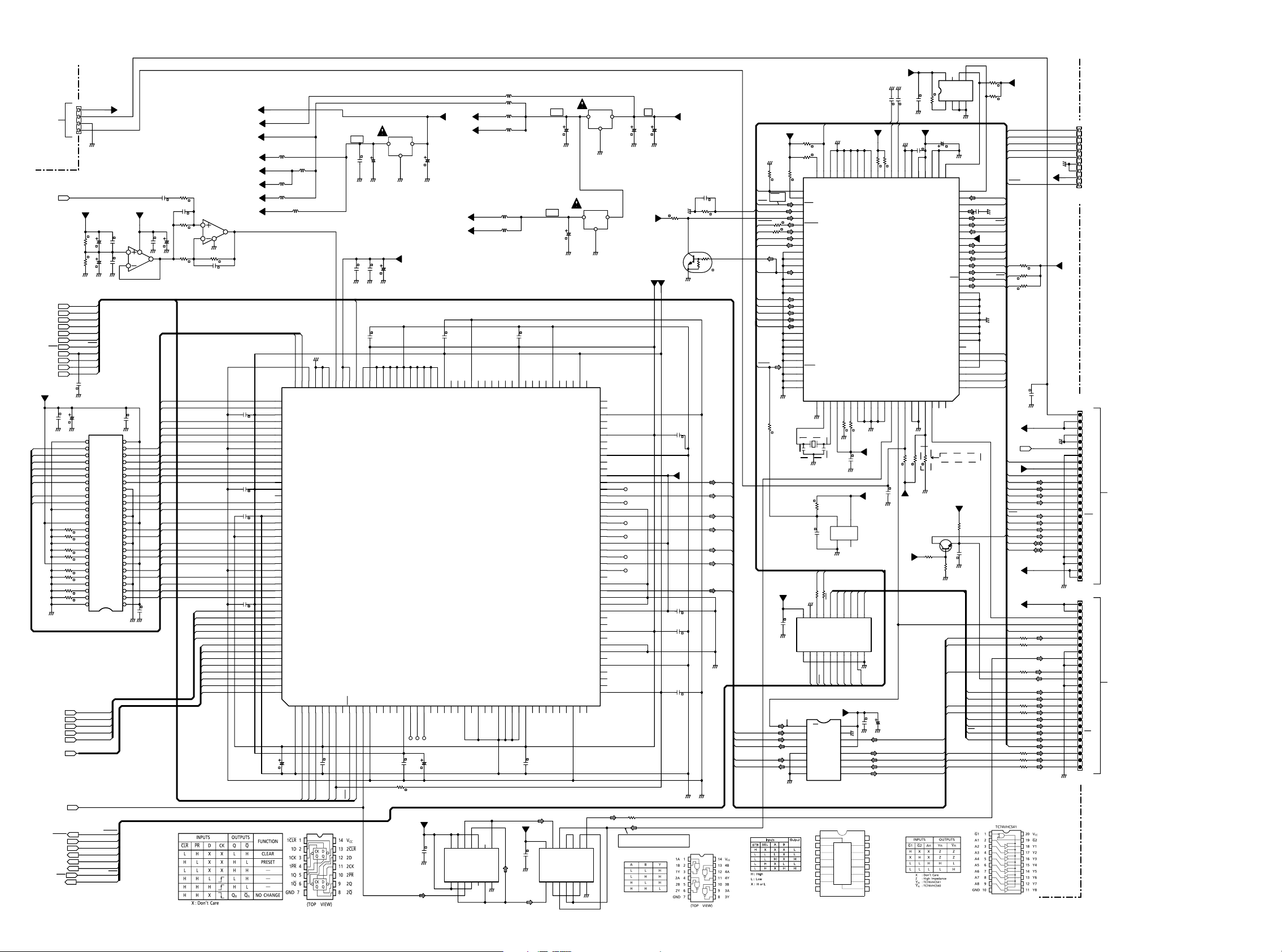
CKT
FROM BUCK UP
RFAC
FROM RF IC(Q110-1)
DECMNT2
XMSLAT
MSCK
MSDTO
MSDTI
MSRADY
XRST
SMUT
PCMD
BCK
LRCK
D3.3DI
0.1u
C236
GND GND
A4
A5
A6
A7
A8
A9
DCKE
DCLK
R235
R236
R237
R238
R239
R240
R241
R242
GND
REQST
XSHD
SDCK
XSAK
SDEF
VDT[0-7]
768FS
DRVRST
DRVRDY
DRVRQI
DRVTXI
DRVRX
DRVCLK
SEEK
-ATT
J109
C235
22/6.3
10k
10k
10k
10k
10k
10k
10k
10k
4
3
2
1
A5V
15k5.1k
R227R228
GND GND GND
DECMNT2
XMSLAT
MSDTO
MSDTI
MSRADY
C222
GND
26272829303132333435363738394041424344454647484950
MSCK
PCMD
GND
XRST
SMUT
LRCK
0.1
768FS
C228C229
BCK
22/6.322/6.3
Q122
EM636165TS-7
REQST
XSHD
SDCK
XSAK
SDEF
VDT[0-7]
DRVRST
DRVRDY
DRVRQI
DRVTXI
DRVRX
DRVCLK
5VU
RFAC
0.1
C226
3
OP-AMP1/2
0.1
C227
2
C256
GND
12345678910111213141516171819202122232425
GND
SEEK
-ATT
PV16 SERVO (3/3)
5VU
FC
L132
FC
107
(NC)IDIN5
TCK
106
105
BSIO3(GND)
(NC)TDI
L133
L121
L123
L125
L124
104
103
102
101
100
(NC)IDIN4
(NC)IDIN3
(NC)IDIN2
(NC)IDIN1
(NC)IDIN0
VSC1(GND)
TRST
TEST1
(NC)TDO
(NC)TMS
3334353637383940414243
GND
(NC)IHOLD
VDC4(2.5V)
TEST3
VDC1(2.5V)
0.1
C239
D3.3DI
0.1
C346
GND
(NC)IPLAN
(NC)UBIT
Q140
3.3V
GND
2.6V
(NC)IERR
(NC)IBCK
VSC4(GND)
(NC)IANCI
(NC)XBIT
(NC)SUPDT0
(NC)SUPDT1
(NC)SUPDT2
14 8910111213
TC74VHC00FT
1234567
FC
FC
0.1
C246
9998979695949392919089
(NC)IVLD
TEST2
A5V
D5VDV
D3.3DV
L122
A3.3DV
D3.3CD
R230
C225
0.01
2k
C232
C230
GND GND
1
XRASD
XCASD
XWE
1U
C259
0.1
A3
A2
A1
A0
A10
A11
DQ7
DQ6
DQ5
DQ4
DQ3
DQ2
DQ1
DQ0
C231
100/6.3
DQ5
DQ4
DQ3
DQ2
DQ1
DQ0
DCLK
DCKE
XWE
XCASD
XRASD
A11
A10
A9
A8
A7
A6
A5
A4
A3
A2
A1
A0
2p
R231
5
3k
OP-AMP2/2
6
R229
R232
2k 3k
C233
REQST
XSHD
SDCK
XSAK
SDEF
VDT[0]
VDT[1]
VDT[2]
VDT[3]
VDT[4]
VDT[5]
VDT[6]
VDT[7]
GND
A5V
8
Q121
AD8062
0.1
GND
A3.3CD
M3.3V
A3.3V
Q121
AD8062
WARFI
7
4
2p
0.1
C252
0.1
C253
0.1
C254
0.1
C255
L128
L129
133
134
135
136
137
138
139
140
141
142
143
144
145
146
147
148
149
150
151
152
153
154
155
156
157
158
159
160
161
162
163
164
165
166
167
168
169
170
171
172
173
174
175
176
Q123
CXD2752R
DQ5
DQ4
VDIO(3.3V)
DQ3
DQ2
DQ1
DQ0
VDIO5(GND)
DCLK
DCKE
XWE
XCAS
XRAS
VDIO6(3.3V)
A12
A11
A10
VSC6(GND)
A9
A8
VDC6(2.5V)
A7
A6
A5
A4
VDIO6(GND)
A3
A2
A1
A0
VDIO7(3.3V)
XSRQ
XSHD
SDCK
XSAK
SDEF
SD0
SD1
SD2
SD3
SD4
SD5
SD6
SD7
Q141
L120
C234
22/6.3
L126
DQ7
DQ6
GND
132
131
130
129
DQ8
DQ7
VSIO4(GND)
WAVVSS1(GND)
VSCO(GND)
XMSLAT
MSCK
MSDATI
123456789
MSDTO
MSCK
XMSLAT
TC74VHC74FT
128
127
WAVRB
WAVVSS0(GND)
VDCO(2.5V)
MSDATO
0.1
C237
MSDTI
MSRADY
3.3V
0.1
C343
GND
0.1
C249
GND GND GND
DECMNT2SMUT
126
125
124
123
122
WCK
WARFI
WAVDD1(2.5V)
WAVVDD0(2.5V)
MSRADY
(NC)MSDOE
XRST
XMUT
1011121314151617181920212223242526272829303132
XRST
768FS
Q152
NJM2391DL1-33
3.3V 1A
INOUT
13
2
C342
100/6.3v
GND GND
A2.6DS
C251
22/6.3
COM
GND
DSD MULTI DECORDER
0.1 1u
C248 C250
121
120
119
118
117
116
115
114
R243
WAD5
(NC)LRCKI
WAD4
VCS5(GND)
(NC)F75HZ
VDIO0(3.3V)
0.1
C238
10k
113
WAD3
WAD2
TESTI
MNT0
MNT1
MNT2
DSDM0
DSDM1
DSDM2
D3.3DI
0.1
C344
GND
WRFD
VDC5(2.5V)
DSD768fs
VSIO0(3.3V)
WAD7
WAD6
EXCKO1(384fs)
EXCKO2(256fs)
C345
100/6.3
0.1
C247
112
111
110
WAD1
WAD0
VDIO4(3.3V)
(NC)MNT3
(NC)MNT4
(NC)MNT5
C260
100/6.3
14 8910111213
Q141
TC74VHC74FT
1234567
A5V
D2.6DS
A2.6DS
109
(NC)IDIN7
(NC)MNT6
D3.3DS
D3.3DI
108
(NC)IDIN6
(NC)MNT7
NJM2391DL1-33
C339
22/6.3
NJM2391DL1-26
C340
22/6.3
GND GND
(NC)IOTE
(NC)IFRAN
(NC)IEMPTY
(NC)IFULL
VDIO3(3.3V)
(NC)IANCO
VSIO2(GND)
(NC)IOUT5
(NC)IOUT4
VDC3(2.5V)
(NC)IOUT3
(NC)IOUT2
VDC3(GND)
(NC)IOUT1
(NC)IOUT0
VDDSD(3.3V)
DSARS
ZDFRS
DSALS
ZDFLS
VDDSD1(GND)
DSALF
ZDFLFE
VDDSD(3.3V)
DSAR
ZDFR
DSAL
DSFL
(NC)PHREFO
PHREFI
BCKAO
BCKA1
VSDSDO(GND)
BCKASL
(NC)DSD2
(NC)DSD1
VDC2(2.5V)
(NC)BCKDO
BCKDI
BCKDSL
(NC)MUDAT
VSC2(GND)
(NC)SUPEN
(NC)SUPDT7
(NC)SUPDT6
VDIO2(3.3V)
(NC)SUPDT3
VSIO1(GND)
(NC)SUPDT4
(NC)SUPDT5
44
384/192
GND
2.6V
DSAC
ZDFC
Q153
2
Q151
3.3V 1A
2
GND
13
COM
INOUT
13
COM
88
87
86
85
84
83
82
81
80
79
78
77
76
75
74
73
72
71
70
69
68
67
66
65
64
63
62
61
60
59
58
57
56
55
54
53
52
51
50
49
48
47
46
45
5V
INOUT
C336
C337
100/6.3
100/6.3
GND GND
5VU
D2.6DS
D3.3DI
ZDFRS
ZDFLS
ZDFLFE
ZDFC
ZDFR
ZDFL
R350
10
SA=CUSTOM IS LOW, NOMAL IS HIGH
CD=ALL TIME LOW
Q140
TC74VHC00FT
47k
RF18
C245
0.1
D3.3DS
C242
0.1
C241
0.1
C240
0.1
+5B
CF09
0.1
GND
1
3
QF03
DTC144EUA
GND
DSDG3 DSDG2
5VU
GND
4.7k
RF12
FMD2
SEEK:L
PLAY:H
RF20
47k
2
DSARS
DSALS
DSALF
DSAC
DSAR
DSAL
BCKAD
DSDG1
SEEK
STBSW
STBSW
0
RF19
DRVRST
DRVRDY
RF13
0
DRVRQI
-ATT
RC5S
CDLED
SALED
SRLED
STBLED
DISPLED
MSRST
GND
1k
RF01
POWER STNDBY
MASTER RESET
D3.3DI
C310
0.1
GND
Q137
TC74VHC541FT
MODE1(CD/SA SELECT)
CD=L,SA=H
PCMD
DSAL
DAPC
DSAR
DARD BCKAD
GND
FMD0
RF04
47k
GND
47k
RF05
RF06
47k
50
GND
GND
GND
MODE1
MODE2
MODE3
HWSTBY
SEEK
STBSW
IR
DRVRES
DRVRDY
DRVRQ
-ATT
GND
60 59 58 57 56 55 54 53 52 51
GND
GND
IRIN
GND
GND
GND
CDLED
SALED
SRLED
STBLED
DISPLED
GND
GND
GND
GND
GND
RESET
GND
GND
GND
80 79 78 77 76 75 74 73 72 71 70 69 68 67 66 65 64 63 62 61
CF02
20 111213141516171819
12345678910
GND
81
GND
12
3
XF01
GND
8MHZ
RF02
330K
0.1
GND
DRVRX
DRVCLK
0
0
R347
RST
GND
R349
DRVRXO
DRVCLO
RSTD
M43D
SA/CD
PCMD
LRCK
DSAL
CMOD
DAPC
DALR
HM1
BCK
DSAR
DSCK
DARD
87654321
DACK
Q126
TC74VHC157FT
1
SEL
2
1A
3
1B
4
1Y
5
2A
6
2B
7
2Y
8
GND
VCCX1X0
848382
4.7k
RF07
GND
1
4
M2
M43
M2D
M3D
D3.3DS
161514131211109
AGS
B
YB
A
B
YBY
CF05
GND
A
Y
A
0.1
M3
M42D
GND
100k
RF08
2
3
M42
M41D
GND
GND
GND
5VU
QF02
S-80843ALNP
4.3V
GND
GND
GNDGND
0.1
0.1
CF12
CF11
KEY1
KEY0
5VU
KEY0
KEY1
GND
47k
47k
RF17
RF16
GND
GND
GND
GND
GND
5VU
M41
0.1
C294
V
16
CC
15
STB
14
4A
4B
13
12
4Y
11
3A
10
3B
9
3Y
GND
KEY3
QF01
GND
CF06
C295
MB90F553A
GND
KEY1
KEY2
FLASH U-COM
SYCLSW
GND
22/6.3 0.1
KEY0
MODE1
AGND
STBY
5VU
10k
RF09
A5V
CF10
CF04
AREFQ
GND
0.1
GND
5VU
1u
353637383940414243444546474849
AVREF
GND
100k
RF10
GND
Q137 TC74VHC541FTQ126 TC74VHC157FT
10k
RF23
CF08
22/6.3
34
GND
AVDD
LPFSW
MODE2GND
999897969594939291908988878685
0HM
0
RF11
QF05 R351
NC
R352
NC
LRCK
DALR
BCK
DACL
8765
AT24C04N
1234
313233
GND
EECLK
EEDAT
CDOUT
CDIN
CAP
CDCLK
CDRST
DRVTX
DRVRX
DRVCLK
VRDAT
FDAT
FCLK
FRST
FCEN
GND
GND
GND
GND
GND
GND
GND
GND
MUT2
MUT1
GND
M43
M42
M41
OPEN
OPEN
100
OPTION
SACD STERED : 0 OHM
SACD MULTI : DELETE
123
CBE
NC
R353
GND
DAPC
DARD
DACL
DSALS
DSARS
DALR
DSALF
DSAC
QF04
GND
D3.3DI
GND
RF22
10k
5VU
RF21
10k
GND
CF03
21 22 23 24 25 26 27 28 29 30
1 2 3 4 5 6 7 8 91011121314151617181920
22K
2200p
CF13
M41
M42
M2
M3
RST
M43
FCLK
FDAT
WRDAT
FMD0
FMD2
MSRST
M0D
M3D
0.1
GND
M2D
RSTD
DRVTXI
5VU
DRVRXO
DRVCLO
WRDAT
47k
RF03
FDAT
FDAT
FCLK
47k
RF15
M0D
FRES
47k
RF14
M3D
FCEN
GND
MUT2
MUT1
M43D
M42D
M41D
M0D
DIGO
RC5S
STBSW
CDLED
SALED
SRLED
STBLED
DISPLED
FRES
FCEN
FCLK
FDAT
KEY1
KEY0
A5V
+5B
MUT1
R361
R360
R359
R358
R357
MUT2
R356
R355
R354
0.1
GND
P8V
DIGO
5VU
47
47
47
47
47
47
47
47
9
8
7
6
5
GND
4
CONNECTOR
3
5VU
2
FOR MP-WRITING
1
J110
A5V
CF07
J105
WF04
25
+12v
24
+8
23
+8
22
MGN
21
MGN
GND
20
DIGO
19
GND
18
RC5S
17
BK5V
16
STBSW
15
CDLED
14
SALED
13
SRLED
12
STBLED
11
10
DSDG1
25
24
23
22
21
20
19
18
17
16
15
14
13
12
11
10
DSDG1
DISPLED
FRES
9
FCEN
8
FCLK
7
FDAT
6
KEY1
5
KEY0
4
GND
3
GND
2
+5A
1
+5A
J106
+5B
+5B
LPFSW
MODE
MUT1
DAPC
DARD
GND
SYCL
GND
DACL
M0
GND
M41
M42
DSALS
9
DSARS
8
M2
7
M3
6
RST
5
M43
4
MUT2
3
DALR
2
DSALF
1
DSAC
FRONT DATA POWER
TO MAIN PCB (PP16)
WF05
FOR MAIN PCB (PP16)
DSD DATA OUT AND POWER IN
1615
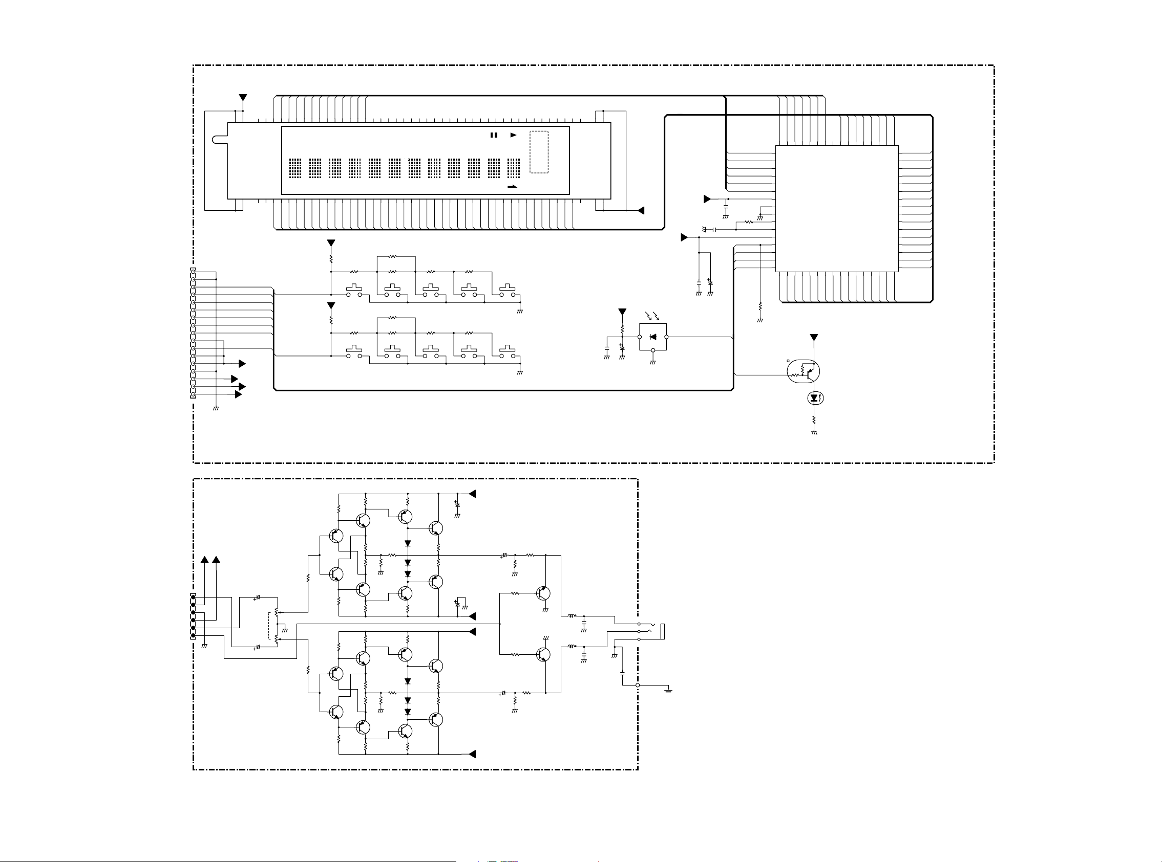
GND
GND
LED_DISP
F_RESET
F_CEN
F_CLK
F_DAT
KEY2
KEY1
RC-5
GND
-VFT
H1
VX01
HQ31302410
1 56789101112131415161718192021222324252627282930313233343536373839404142434445 482 49
JY01
1
2
3
4
5
6
7
8
9
10
5V
11
12
5V
13
5V
14
15
H1
16
17
H2
H1
H2
G[1]
G[2]
G[3]
G[4]
G[5]
G[6]
G[7]
G[8]
G[9]
G[10]
G[11]
G[12]
G[13]
95 53
TIME
P[32]
CD
SACD
2CH
MULTI
P[33]
P[34]
P[35]
P[36]
P[37]
TIMER
DISC
TEXT
P[1]
P[2]
P[3]
P[4]
RNDM
PROG A Ð B
RPT
1
TRK
12 34 56 78 910 1112 1314 1516 1718 1920
P[5]
P[6]
P[7]
P[8]
P[9]
P[10]
P[11]
P[12]
P[13]
P[14]
P[15]
P[16]
P[17]
P[18]
P[19]
P[20]
P[21]
P[22]
P[23]
P[24]
P[25]
P[26]
P[27]
P[28]
P[29]
TTL
P[30]
P[31]
+5V
RY04
1.8K
SY05SY04SY03SY02SY01
PREV
RY10
1.8K
12
12
PAUSE
RY11
1.8K
12
STOP
RY12RY09
12
SY09
12
DIS_OFF
12
TEXT
12
TIME
12
PLAY
SY10
S_MODE
12
D-GND
12
D-GND
+5V
-VFT
DISPLED
FRES
FCEN
FCLK
FDAT
KEY2
KEY1
RC-5
KEY1
KEY2
RY01
2.2K
RY02 RY03 RY06RY05
560 1.8K 5.6K1.8K
+5V
NEXT
RY07
RY08
2.2K
560 5.6K1.8K
SY06 SY07 SY08
OPEN/CLOSE
505154555657585960616163646566676869707172737475767778798081828384858687888990919293949798
G[6]
G[5]
G[4]
G[3]
G[2]
G[1]
464
P[38]
P[39]
P[40]
H2
-VFT
CY04
0.1
CY03
22P
D-GND
+5V
CY02
0.1
CY01
47/6.3V
D-GND
FRES
FCEN
FCLK
FDAT
D-GND
RY13
D-GND D-GND
+5V
RY16
100
CY06
0.1
D-GND D-GND
CY05
47/6.3V
3
2
D-GND
1
ZY01
IR SENSER
RC-5
DISPLED
D-GND
PY16
10K
RY20
D-GND
G[7]
G[8]
G[9]
G[10]
G[12]
G[13]
G[11]
P[39]
P[38]
P[37]
P[36]
P[35]
P[34]
P[33]
AM33
33
AM32
AM31
AM30
AM29
AM28
AM27
AM26
AM25
AM24
AM23
AM22
AM21
AM20
AM19
AM15
AM1312AM1211AM1110AM109AM98AM87AM76AM65AM54AM43AM32AM2
15
14 AM14
13
P[32]
32
P[31]
31
P[30]
30
P[29]
29
P[28]
28
P[27]
27
P[26]
26
P[25]
25
P[24]
24
P[23]
23
P[22]
22
P[21]
21
P[20]
20
P[19]
19
P[18]
AM18
18
AM16
P[17]
AM17
17
16
48G747G846G945
49
G6
50
51
52
53
54
55
VFL
56
57
58
59
60
61
62
63
CL
64
DI
1
P[40]
G1044G1143G1242G1341AA640AA539AA438AA337AA236AA135AM3534AM34
G5
G4
G3
G2
G1
TEST
VSS
OSCO
OSCI
VDD
RES
CE
QY01
LC75712E
AM1
P[9]
P[10]
P[11]
P[12]
P[1]
P[2]
P[3]
P[4]
P[5]
P[6]
P[7]
P[8]
P[13]
P[14]
P[15]
P[16]
10K
+5V
3
RY15
QY05
DTA114ES
1
DY04
DISPLAY OFF
1K
2
D-GND
RCH
-12V
GND
+12V
LCH
TMUT
J902
1
2
3
4
5
6
A-GND
A-GND
C904
A-GND
220/25V
C903
220/25V
+12V
-12V
+12V
-12V
C905
JUMPER
C906
JUMPER
R928
NC
NC
R927
A-GND
R941
NC
R942
NC
A-GND
R929
JUMPER
Q941
NC
Q942
NC
R930
JUMPER
3
E
B
2
1
C
L901
A-GND
A-GND
2
B
C907
1000p
A-GND
L902
1
C
C908
1000p
3
E
A-GND
A-GND
C909
NC
J903
2
3
1
H.P. OUT
W902
R925
560
R926
560
R923
680
R924
680100
R915
270
3
E
Q909
2
2SA1048
Y.GR
1
D901
D903
D905
1
3
R917
R916
270
3
1
D902
D904
D906
1
3
R918
Q911
2SC2458
Y,GR
270
Q910
2SA1048
Y.GR
Q912
2SC2458
Y,GR
270
1
C
Q913
2
2SC2458
B
Y,GR
3
E
R919
6.8
R921
6.8
3
E
Q915
2
2SA1048
B
Y.GR
1
C
1
C
Q914
2
2SC2458
B
Y,GR
3
E
R920
6.8
R922
6.8
3
E
Q916
2
2SA1048
B
Y.GR
1
C
B
C
C
2
B
E
E
2
B
C
C
2
B
E
R907
R903
5.6k
Q901
2SA1048
E
Y.GR
2
B
2
B
Q903
2SC2458
Y,GR
Q902
2SA1048
Y.GR
2
B
Q904
2SC2458
Y,GR
R904
5.6k
2
B
C
C
E
E
C
C
E
+12V
-12V
R901
46
A-GND
31
470
5
2
R902
470
C901
100/10V
R950
10k B
C902
100/10V
PR16
330
1
C
2
Q905
2SC2458
B
R905
5.6k
R906
5.6k
Y,GR
3
E
R909
100
R911
100
A-GND
3
E
Q907
2
2SA1048
Y.GR
B
1
C
R913
330
R908
330
1
C
2
Q906
2SC2458
B
Y,GR
3
E
R910
R912
100
A-GND
3
E
Q908
2
2SA1048
Y.GR
B
1
C
R914
330
3
1
1
3
3
1
1
3
17 18
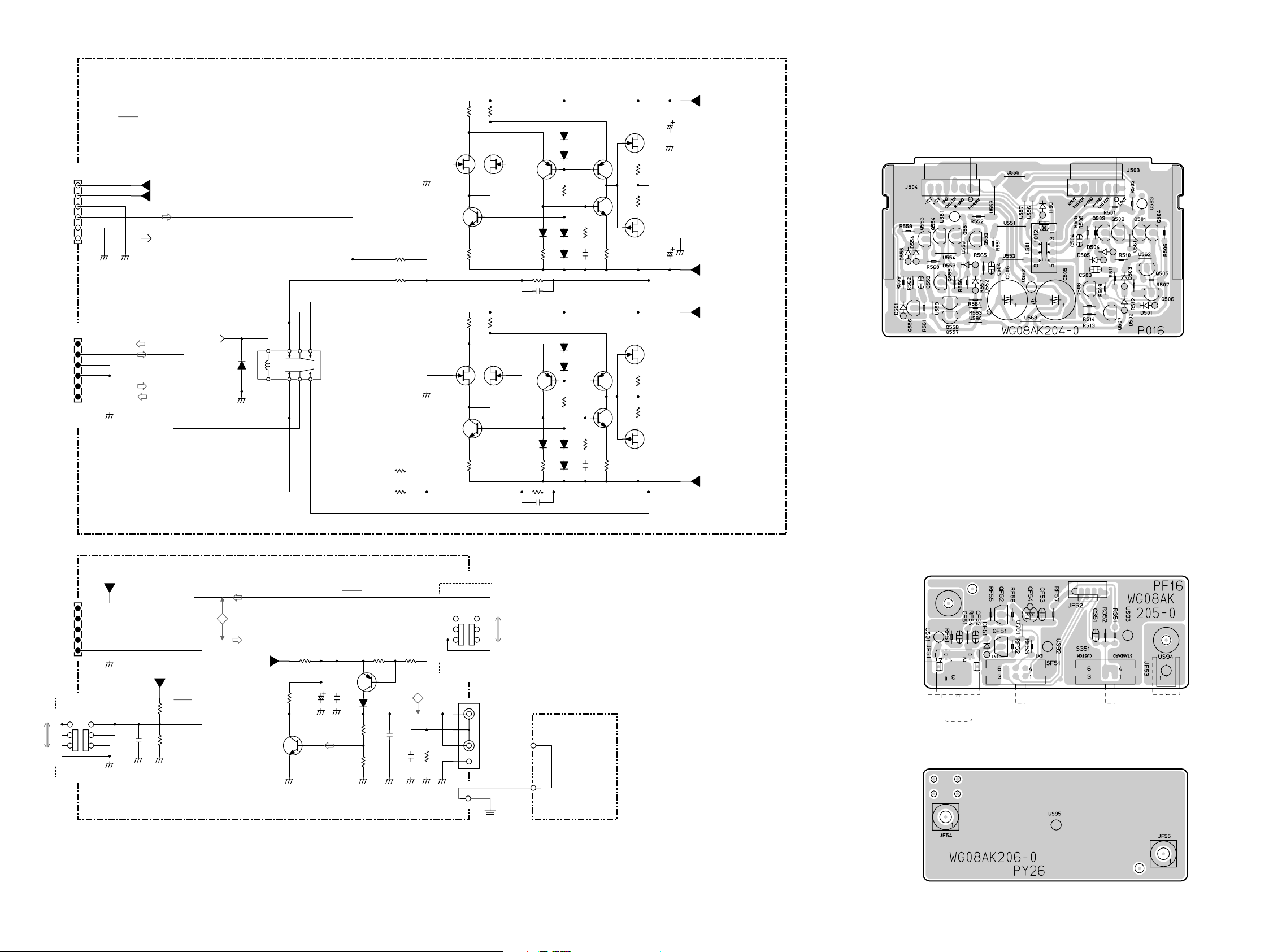
PO16
7. PARTS LOCATION
-12V
+12V
A-GND
CMIXIN
R-GND
PTMDRV
LOUT
LMIXIN
A-GND
A-GND
RMIXIN
ROUT
J503
6
5
4
3
2
1
1
2
3
4
5
6
J504
R-GND
A-GND
LPO
A-GND
-12VA
+12VA
PTMDRV
PTMDRV
D511
R-GND
13
+
-
12 10
98
C505
A-GND
470 16V
ARA
+12VA
-12VA-12VA
+12VA
PO16
Q553 Q554 Q551 Q552 Q503 - Q501 Q504
Q555 - Q558
Q508 - Q505
120
R506
Q501
2SK369 BL
D
+
1
G
S
A-GND
1
Q503
2SC2240
GR,BL
3
R502
22k
R501
10k
120
R556
54
L501
R552
22k
R551
10k
A-GND
Q551
2SK369 BL
+
Q553
2SC2240
GR,BL
D
1
G
S
1
3
120
R507
3
1
G
2
2
S
Q502
2SK369 BL
C
2
B
E
68
R508
120
R557
D
3
3
1
G
2
2
S
Q552
2SK369 BL
C
2
B
E
68
R558
-
-
GR,BL
R515
C504
Q554
2SA970
GR,BL
R565
C554
D501
R509
D551
R559
3
1
560
3
1
560
Q504
D
2SA970
3
D502
E
D503
2
B
C
10k
10p
E
C
10k
10p
D504
D505
2
D554
D555
2SC2240
33k
R510
R511
100
C503
47p
D552
D553
B
2SC2240
33k
R560
100
R561
47p
C553
Q505
2SA970
GR,BL
2
B
Q506
GR,BL
2
B
Q555
2SA970
GR,BL
2
B
Q556
GR,BL
2
B
C
R512
C
R562
Q507
2SK170
D
3
V
1
G
E
3
R513
1
C
1
R514
E
3
G
1
Q508
2SJ74
V
560
Q557
2SK170
V
1
G
E
3
R563
1
C
1
R564
E
3
G
1
Q558
2SJ74
V
560
A-GND
2
S
33
33
S
2
ARA
D
3
C506
470 16V
D
3
2
S
33
33
S
2
D
3
STANDARD
CUSTOM
+5VD
GND
RC5S
RC5F
LPFSW
JF52
1
2
3
4
5
S351
654
+5VD2
GND
321
GND
PF16
C351
GND
+5VD2
22k
R351
0.1
GND
R352
LFB
LPFSW
NC
RC-5 IN/OUT
RC5S
9
RC5F
+5VD2
RF56
4.7k
1
3
QF52
2SC2458
C
E
RF57
100
PF16
QF52 QF51
RF53
4.7k
0.1
9
RF51
22
GNDGND
RC-5 INT/EXT SW
SF51
654
EXT
321
INT
JF51
1
RC-5
3
IN/OUT
2
4
GNDGND GND
JF53
EARTH
SHEELDE
JF55
PY26
JF54
PY26
LRA
RF52
3
E
4.7k
2
B
QF51
1
C
2SA1048
0.1
CF54
CF53
10/63V
GND
2
B
GND
DF51
RF54RF55
10k2.2k
CF52
GND
470p
CF51
2019

PA16
QD21 - QD27
Q802
Q821
Q801
Q803
QD60
QD61
QD41
QD71
Q601 Q603 - Q608
Q651 Q653 - Q658
Q401 Q403 - Q408
Q451 Q453 - Q458
Q701 Q703 - Q708
Q751 Q753 - Q758
Q609 Q611 - Q616 Q617 - Q624
Q659 Q661 - Q666 Q667 - Q674
Q409 Q411 - Q416 Q417 - Q424
Q459 Q461 - Q466 Q467 - Q474
Q709 Q711 - Q716 Q717 - Q724
Q759 Q761 - Q766 Q747 - Q474 QT01
21 22

PP16
PY16
QY05 QY01
Q853 Q857
Q851 Q855
Q852 Q856
QY62
QY61
Q831
QN23 QN22 QN21
PR16
Q903 Q907
Q906
Q910
Q908
Q912
Q916Q914
Q904
Q901Q905
Q911 Q915
Q909 Q913 Q941 Q942
Q902
QN33 QN32 QN31
QN43 QN42 QN04 QY63 QY64 QY65
QN06 QN05 QN02 QN01
2423

PV16
QF01 Q153
Q139 QF02
Q102 Q101 Q108 Q107
Q103 Q104 Q109
Q105
Q137
Q121 Q110
Q115 Q106
Q111 Q112
Q123
Q138
Q159 Q160
Q157 Q156
Q132 Q133
Q124
Q125
Q136 Q135
Q134
PV16
Q129 Q155
Q127
Q140Q141Q128 Q158
Q119
Q126
Q118
Q113 Q114
QF04
QF03
Q151Q122
Q152
Q117Q116
25 26

8. MICROPROCESSOR AND IC DATA
Q116 : CXD3068Q
Pin Description
Pin NoSymbol I/O Description
1 DVDD0 — Digital power supply.
2 XRST I System reset. Reset when low.
3 MUTE I Mute input (low: off, high: on)
4 DATA I Serial data input from CPU.
5 XLAT I Latch input from CPU. Serial data is latched at the falling edge.
6 CLOK I Serial data transfer clock input from CPU.
7 SENS O 1, 0 SENS output to CPU.
8 SCLK I SENS serial data readout clock input.
9 ATSK I/O 1, 0 Anti-shock input/output.
10 WFCK O 1, 0 WFCK output.
11 XUGF O 1, 0 XUGF output. MNT0 or RFCK is output by switching with the command.
12 XPCK O 1, 0 XPCK output. MNT1 is output by switching with the command.
13 GFS O 1, 0 GFS output. MNT2 or XROF is output by switching with the command.
14 C2PO O 1, 0 G2PO output. MNT3 or GTOP is output by switching with the command.
15 SCOR O 1, 0 Outputs a high signal when either subcode sync S0 or S1 is detected.
16 C4M O 1, 0 4.2336MHz output. 1/4 frequency division output for V16M in CAV-W mode or variable pitch mode.
17 WDCK O 1, 0 Word clock output. f = 2Fs. GRSCOR is output by the command switching.
18 DVSS0 — — Digital GND.
19 COUT I/O 1, 0 Track count signal I/O.
20 MIRR I/O 1, 0 Mirror signal I/O.
21 DFCT I/O 1, 0 Detect signal I/O.
22 FOK I/O 1, 0 Focus OK signal I/O.
23 PWMI I Spindle motor external control input.
24 LOCK I/O 1, 0 GFS is sampled at 460Hz; when GFS is high, this pin outputs a high signal. If GFS is low eight consecutive samples,
this pin outputs low. Input when LKIN = 1.
25 MDP O 1, Z, 0 Spindle motor servo control output.
26 SSTP I Disc innermost track detection signal input.
27 FSTO O 1, 0 2/3 frequency division output for XTAI pin.
28 DVDD1 — — Digital power supply.
29 SFDR O 1, 0 Sled drive output.
30 SRDR O 1, 0 Sled drive output.
31 TFDR O 1, 0 Tracking drive output.
32 TRDR O 1, 0 Tracking drive output.
33 FFDR O 1, 0 Focus drive output.
34 FRDR O 1, 0 Focus drive output.
35 DVSS1 — — Digital GND.
36 TEST I Test. Normally, GND.
37 TES1 I Test. Normally, GND.
38 VC I Center voltage input.
39 FE I Focus error signal input.
40 SE I Sled error signal input.
41 TE I Tracking error signal input.
42 CE I Center servo analog input.
43 RFDC I RF signal input.
44 ADIO O Analog Test. No connected.
45 AVSS0 — — Analog GND.
46 IGEN I Constant current input for operational amplifi er.
47 AVDD0 — — Analog power supply.
48 ASYO O 1, 0 EFM full-swing output. (low = Vss, high = VDD)
49 ASYI I Asymmetry comparator voltage input.
50 RFAC I EFM signal input.
51 AVSS1 — — Analog GND.
52 CLTV I Multiplier VCO1 control voltage input.
53 FILO O Analog Master PLL fi lter output (slave = digital PLL).
54 FILI I Master PLL fi lter input.
55 PCO O 1, Z, 0 Master PLL charge pump output.
56 AVDD1 — — Analog power supply.
57 BIAS I Asymmetry circuit constant current input.
58 VCTL I Wide-band EFM PLL VCO2 control voltage input.
Wide-band EFM PLL VCO2 oscillation output. Serves as wide-band EFM
59 V16M I/O 1, 0 PLL clock input by switching with the command.
60 VPCO O 1, Z, 0 Wide-band EFM PLL charge pump output.
61 DVDD2 — — Digital power supply.
62 ASYE I Asymmetry circuit on/off (low = off, high = on).
63 MD2 I Digital Out on/off control (low = off, high = on).
64 DOUT O 1, 0 Digital Out output.
65 LRCK O 1, 0 D/A interface. LR clock output. f = Fs
66 PCMD O 1, 0 D/A interface. Serial data output (two's complement, MSB fi rst).
67 BCK O 1, 0 D/A interface. Bit clock output. Outputs a high signal when the playback disc has emphasis, and a low
68 EMPH O 1, 0 Outputs a high signal when the playback disc has emphasis, and a low signal when there is no emphasis.
69 XTSL I Crystal selection input. Low when the crystal is 16.9344MHz; high when it is 33.8688MHz.
70 DVSS2 — — Digital GND.
71 XTAI I Crystal oscillation circuit input. When the master clock is input externally,
input it from this pin.
72 XTAO O Crystal oscillation circuit output.
73 SOUT O 1, 0 Serial data output in servo block.
74 SOCK O 1, 0 Serial data readout clock output in servo block.
75 XOLT O 1, 0 Serial data latch output in servo block.
76 SQSO O 1, 0 Sub-Q 80-bit, PCM peak or level data outputs. CD TEXT data output.
77 SQCK I SQSO readout clock input.
78 SCSY I GRSCOR resynchronization input.
79 SBSO O 1, 0 Sub-Q P to W serial output.
80 EXCK I SBSO readout clock input.
Notes)
PCMD is a MSB fi rst, two’s complement output.
XUGF is the frame sync obtained from the EFM signal, and is negative pulse. It is the signal before sync protection.
XPCK is the inverse of the EFM PLL clock. The PLL is designed so that the falling edge and the EFM signal transition point
coincide.
The GFS signal goes high when the frame sync and the insertion protection timing match.
C2PO represents the data error status.
2827

Q116 : CXD3068Q
XTAI
XTSL
XTAO
71 72
27
FSTO
C4M
RFAC
ASYI
ASYO
ASYE
BIAS
XPCK
FI LO
FI LI
PCO
CLTV
MDP
LOCK
PWMI
SENS
DATA
XLAT
CLOK
SCOR
SBSO
EXCK
SCSY
SQSO
SQCK
RFDC
IGEN
16
50
49
48
62
57
12
53
54
55
52
25
24
23
7
4
5
6
15
79
80
78
76
77
43
CE
42
TE
41
SE
40
FE
39
VC
38
46
Clock
Generator
Asymmetry
Corrector
Digital
PLL
Digital
CLV
CPU
Interface
OPAmp
Analog SW
V16M
6069
59
Converter
44
VPCO
A/D
DCK
FCK
W
EMPH
VCTL
58
GFS
XUGF
13
11
EFM
demodurator
Sub Code
Processor
Servo
Auto
Sequencer
68
10
SERVO
Interface
MIRR
DFCT
FOK
SERVO DSP
FOCUS SERVO
TRACKING
SERVO
SLED SERVO
Error
Corrector
32K
RAM
2PO
RCK
W
C
L
65 66
1417
D/A
Interface
Digital
Signal processor block
PWM GENERATOR
TRACKING PWM
CK
CMD
B
P
67
3
OUT
Servo block
FOCUS PWM
GENERAT OR
GENERAT OR
SLED PWM
GENERATOR
UTE
M
TES1
37
TEST
36
XRST
2
63
MD2
DOUT
64
73
SOUT
74
SOCK
XOLT
75
SCLK
8
COUT
19
SSTP
26
ATSK
9
MIRR
20
21
DFCT
22
FOK
33
FFDR
34
FRDR
TFDR
31
32
TRDR
29
SFDR
30
SRDR
ADIO
Q126 : TC74VHC157
Inputs Output
STB SEL A B
H X X X L
L L L X L
L L H X H
L H X L L
L H X H H
H : High
L : Low
X :
SEL
1A
1B
1Y
2A
2B
2Y
GND
V
1
2
3
4
5
6
7
AGS
B
A
YB
A
B
Y
A
YBY
8
16
15
14
13
12
11
10
CC
STB
4A
4B
4Y
3A
3B
9
3Y
29

Q101 : CXD1881R
Pin Description
Power Supply Pins
Name Type Description
VPA — Power supply pin for the RF block and serial port
VPB — Power supply pin for the servo block
VNA — Ground pin for the RF block and serial port
VNB — Ground pin for the servo block
V33 — Power supply pin for the output buffers
V25 — Reference power supply for the servo output
Input Pins
Name Type Description
DVDRFP, DVDRFN I RF SIGNAL INPUTS: Differential RF signal attenuator input pins.
RFSIN I RF SIGNAL INPUT: Single-ended RF signal attenuator input pin.
AIP, AIN I AGC AMPLIFIER INPUTS: Differential AGC amplifi er input pins.
DIP, DIN I ANALOG INPUTS FOR RF SINGLE BUFFER: Differential analog inputs to the RF single-end output buffer
and full wave rectifi er.
A, B, C, D I PHOTO DETECTOR INTERFACE INPUTS: Inputs from the main beam photo detector matrix outputs.
A2, B2, C2, D2 I PHOTO DETECTOR INTERFACE INPUTS: AC coupled inputs for the DPD from the main beam photo
detector matrix outputs.
CD_A, B, C, D I CD PHOTO DETECTOR INTERFACE INPUTS: CD_A, B, C, D come from the CD main beam photo detector
matrix outputs.
CD_E, F I CD PHOTO DETECTOR INTERFACE INPUTS: CD side beam photo dector outputs and used for the CD
tracking detection.
MIN I RF SIGNAL INPUT FOR MIRROR: AC coupled inputs for the mirror dection circuit from MEVO.
DVDPD I APC INPUT: DVD APC input pin from the monitor photo diode.
CDPD I APC INPUT: CD APC input pin from the monitor photo diode.
LDON I APC OUTPUT ON/OFF: APC output control pin. A high level activates LD output. (open low)
LINK I LINKING SIGNAL INPUT PIN: In the linking area, this pin goes high and the Mirror and TE outputs are
disabled, when the link signal is enabled. (open low)
Output Pins
Name Type Description
ATOP, ATON O DIFFERENTIAL ATTENUATOR OUTPUTS: Attenuator outputs.
FNP, FNN O DIFFERENTIAL NORMAL OUTPUTS: Filter normal outputs.
RFAC O SINGLE-ENDED NORMAL OUTPUT: Single-ended RF output.
RFDC O RF SIGNAL OUTPUT: Single-ended RF summing output reference to VPB-2.4 (V).
FE O FOCUSING ERROR SIGNAL OUTPUT: Focus error output reference to V125.
TE O TRACKING ERROR SIGNAL OUTPUT: Tracking error output reference to V125.
CE O CENTER ERROR SIGNAL OUTPUT: Center error output reference to V125.
MEVO O RFDDC BOTTOM ENVELOPE OUTPUT: Bottom envelope, PI or bottom clamped RF envelope signal output for
mirror detection.
DFT O DEFECT OUTPUT: CMOS output (V33 or VPB). When the PI signal level is below the detection level or when
the RF signal level is below the detection level, the DFT output goes high. This output is selected by serial port.
MIRR O MIRROR DETECT OUTPUT: Mirror detect comparator output. CMOS output (V33 or VPB).
PI O PULL-IN SIGNAL OUTPUT: The summing signal output of A, B, C, D, or CD_A, B, C, D. Reference to V25/3.
DVDLD O APC OUTPUT: DVD APC output pin to control the laser power.
CDLD O APC OUTPUT: CD APC output pin to control the laser power.
MNTR O MONITOR OUTPUT: Monitor output signal is selected by PIOR bit7-5.
Serial Port Pins
Name Type Description
SDEN I SERIAL DATA ENABLE: Serial enable CMOS input. A high level input enables the serial port. (not to be left open)
SDATA I/O SERIAL DATA: Serial data bidirectional CMOS pin(V33 or VPA). NRZ programming data for the internal registers is
applied to this input. (not to be left open)
SCLK I SERIAL CLOCK: Serial clock CMOS input. The clock applied to this pin is synchronized with the data applied to SDATA.
(not to be left open)
30

Analog Pins
Name Type Description
BYP — The RF AGC integration capacitor CBYP, is connected between BYP and VPA.
CP — DIFFERENTIAL PHASE TRACKING LPF PIN: The external capacitance is connected between CN.
CN — DIFFERENTIAL PHASE TRACKING LPF PIN: The external capacitance is connected between CP.
LCP — LENS SHIFT OFFSET CANCEL LPF PIN: The external capacitance is connected between LCN.
LCN — LENS SHIFT OFFSET CANCEL LPF PIN: The external capacitance is connected between LCP.
MP — MIRR TOP HOLD PIN: The external capacitance is connected to VPB.
MB — MIRR BOTTOM HOLD PIN: The external capacitance is connected to VPB.
MEV — RFDC BOTTOM ENVELOPE PIN: The external capacitance is connected to VPA.
MLPF — MIRROR LPF PIN: An external capacitance is connected to VPB.
TPH — PI TOP HOLD PIN: An external capacitance is connected to VPB.
VC — REFERENCE VOLTAGE OUTPUT: This pin provides the DC bias reference voltage (VPB/2). Output impedance is less
than 50 Ω.
V125 — REFERENCE VOLTAGE OUTPUT: DC bias voltage output and it is also used for servo output reference. (V25/2)
RX — REFERENCE RESISTOR INPUT: An external 12.0 k&, 1 % resistor is connected from this pin to ground to establish a
precise PTAT (proportional to absolute temperature) reference current for the fi lter.
Q101 : CXD1881R
1
DVDRFP
DVDRFN
RFS I N
CD_A
CD_B 15
CD_C 14
CD_D 13
CD_E
CD_ F 17
DVDPD
CDPD
A2
B2
C2
D2
A
B 11
C
D
2
63
12
16
10
9
18
3
4
5
6
23
24
MUX
INPUT
SEL
MUX
CD/DVD
12dB is added
@ h i g h g a i n mo d e
From S-port
LD H/ L
2
INPUT IMP
SEL
A
B
C
D
12dB is added
@ high gain mode
6dB is added
@ high gain mode
GCA
GCA
3
S-PORT
GCA
EQ
GCA
EQ
GCA
EQ
GCA
EQ
3
FROM
S-PORT
APC SEL
DVD/ CD
Dua l APC
26
LDON
62 61 60 59
ATT
4
ATT
W/LPF
GCA
W/LPF
GCA
W/LPF
GCA
W/LPF
GCA
12dB is added
@ high ga i n mode
GCA
GCA
GCA
GCA
3
S-PORT
FROM
VC
3
22
CDLD
FNP
ATOP
ATON
AIN
AIP
AGC
INPUT
BIAS
2
INPUT IMP
SEL
SSOUT
SIGDET
B+D
SUM
Amp .
A+C
A+D
B+C
FROM
4dB
GCA SEL
4
FROM
S-PORT
Comp .
PHASE
DETECTOR
PHASE
DETECTOR
Sink current
From S-port
2
BOTTOM
ENVELOPE
50
MEV
Pl l
MUX
32
MEVO
AGCO
21
DVDLD
Clamp
& Env
2
TOPHOLD
TOPHOLD
+3dB
Input lmp
From S-port
2
INPUT
BUFF
31
MIN
PROGRAMMABLE
DIFFERENTIATOR
Leve l
DAC
4dB
GCA
Mi r r ga in
From S-port
2
53 52
EQUAL I ZER
FILTER
FROM
4
S-PORT
70kHz
LPF
6dB
Amp
CE - ATT
CEPOL
Disk det &
Mi r r LPF
From S-por t
30
MLPF
FNN
DIN
DIP
55 54 57
FULL WAVE
RECT I F I ER
OUTPUT INHIBIT
FROM S-PORT
AGCO
70kHz 6dB, 4b i t
LPF GCA
FROM
5
S-PORT
Of f set
cansel
BCA DET
FROM
S-PORT
- 6dB @ n o r ma l
Buf f
Of f set
cansel
4
FROM
S-PORT
LPF
3
ATT
Po l se l .
buf f(-12dB)
SUBMUX
LPF GCA
CEFDBCD/ DVDCP / CN
Low lmp
CONTROL
Signals
To each block
Comp
hys & off set
From S-por t
MIRR
COMP
PEAK /
BOTTOM
HOLD
28
MB29MP
Internal
FDCHG
LINKEN
FROM
S-PORT
5
Of f set
cansel
TOPHLD
DAC
2
GCA
6dB, 4b i t
PI
FE
TE
CE
V25
V125
V25 / 3
Of f set
cansel
6
FROM
S-PORT
for servo output ref.
VCI fo rservo input
LINK
RFAC
AGC HOL D
FAST A t t a c k o f f
AGC
CHARGE
PUMP
COMP
MNTR
Cn t r l
HLDEN
3
FROM
S-PORT
VC=VP B / 2
SERI A L PORT
REGI STER
27
58
VPA
MIRR
SEL
TE
RST
V25 /2
V33 f or
out pu t buf f
19
VPB
VNA51VNB
56
BYP
49
RX
40
FE
Pl l
38
PI
35
TPH
34
DFT
61
RFDC
41
CE
42
MNTR
44
LCP
43
LCN
7
CP
8
CN
39
TE
37
V25
36
V125
20
VC
48
SDEN
47
SDATA
46
SCLK
45
V33
2533
31

Q123 : CXD2752R
Pin Symbol I/O Description No.
1 VSC — Core GND.
2 XMSLAT I Latch input for microcomputer serial communication. The address and data are atched at the fall of this pin.
3 MSCK I Shift clock input for microcomputer serial communication. The serial input data is loaded and shifted at the rise
of the clock input to this pin. During readout, the readout data changes at the fall of the clock input to this pin.
4 MSDATI I Data input for microcomputer serial communication. The data and address are serially input from the
microcomputer.
5 VDC — Core power supply. Supply +2.5V.
6 MSDATO O Data output for microcomputer serial communication. Hi-Z other than during output.
7 MSREADY O Output ready fl ag for microcomputer serial communication. Low output when ready. Open drain.
8 XMSDOE O Output enable for microcomputer serial communication. When an external tri-state buffer is used, the buffer is
activated by this pin. Low during MSDATO output.
9 XRST I Reset. The entire IC is reset when low. However, the clock output from the EXCKO1, EXCKO2 and LRCK output
pins does not stop even when reset.
10 SMUTE I Soft mute. Audio output is soft muted when high; mute off when low.
11 MCKI I Master clock input. Input a 768Fs (33.8688MHz) clock.
12 VSIO — I/O GND.
13 EXCKO1 O External output clock 1. 768Fs/512Fs/256Fs/128Fs is output according to the setting.
14 EXCKO2 O External output clock 2. 768Fs/512Fs/256Fs/128Fs is output according to the setting.
15 LRCK O 1Fs (44.1kHz) clock output.
16 FRAME O Frame signal output.
17 VDIO — I/O power supply. Supply +3.3V.
18 MNT0 O Monitor output. Outputs a part of internal operation according to the microcomputer setting.
19 MNT1 O Monitor output. Outputs a part of internal operation according to the microcomputer setting.
20 MNT2 O Monitor output. Outputs a part of internal operation according to the microcomputer setting.
21 MNT3 O Monitor output. Outputs a part of internal operation according to the microcomputer setting.
22 TESTO O Test output. Leave open.
23 TESTO O Test output. Leave open.
24 TESTO O Test output. Leave open.
25 TESTO O Test output. Leave open.
26 TCK I Test clock input. Fix to low.
27 TDI Ipu Test input (pulled up). Leave open.
28 VSC — Core GND.
29 TDO O Test output. Leave open.
30 TMS Ipu Test input (pulled up). Leave open.
31 TRST Ipu Test reset (pulled up). Input the power-on reset signal or fi x to low.
32 TEST1 I Test input. Fix to low.
33 TEST2 I Test input. Fix to low.
34 TEST3 I Test input. Fix to low.
35 VDC — Core power supply. Supply +2.5V.
36 TESTO O Test output. Leave open.
37 XBIT O DST related monitor. No connected. For detailed information, see the DST_X_Bit item in Part 3 of the SACD
Format Book.
38 SUPDT0 O Supplementary data output. (LSB)
39 SUPDT1 O Supplementary data output.
40 SUPDT2 O Supplementary data output.
41 SUPDT3 O Supplementary data output.
42 VSIO — I/O GND.
43 SUPDT4 O Supplementary data output.
44 SUPDT5 O Supplementary data output.
45 VDIO — I/O power supply. Supply +3.3V.
46 SUPDT6 O Supplementary data output.
47 SUPDT7 O Supplementary data output. (MSB)
48 XSUPAK O Supplementary data acknowledge output.
49 VSC — Core GND.
50 TESTO O Test output. Leave open.
51 TESTI I Test input. Fix to low.
52 TESTI I Test input. Fix to low.
53 TESTO O Test output. Leave open.
54 VDC — Core power supply. Supply +2.5V.
55 TESTO O Test output. Leave open.
56 TESTO O Test output. Leave open.
57 BCKASL I Bit clock input/output selection for DSD data output. Low = input (slave), high = output (master).
58 VSDSD — DSD data output GND.
59 BCKAI I Bit clock input for DSD data output. Input the bit clock to this pin when BCKASL = low.
60 BCKAO O Bit clock output for DSD data output. The bit clock is output from this pin when BCKASL = high.
32

61 PHREFI I Phase reference signal input for DSD output phase modulation.
62 PHREFO O Phase reference signal output for DSD output phase modulation.
63 ZDFL O Lch zero data detection fl ag (when set by the microcomputer). Goes high when silent data continues for 300ms.
64 DSAL O Lch DSD data output.
65 ZDFR O Rch zero data detection fl ag (when set by the microcomputer). Goes high when silent data continues for 300ms.
66 DSAR O Rch DSD data output.
67 VDDSD — Power supply for DSD data output. Supply +3.3V separated from other digital power supplies.
68 ZDFC O Cch zero data detection fl ag (when set by the microcomputer). Goes high when silent data continues for 300ms.
69 DSAC O Cch DSD data output.
70 ZDFLFE O LFEch zero data detection fl ag (when set by the microcomputer). Goes high when silent data continues for
300ms.
71 DSALFE O LFEch DSD data output.
72 VSDSD — GND for DSD data output.
73 ZDFLS O LSch zero data detection fl ag (when set by the microcomputer). Goes high when silent data continues for
300ms.
74 DSALS O LSch DSD data output.
75 ZDFRS O RSch zero data detection fl ag (when set by the microcomputer). Goes high when silent data continues for
300ms.
76 DSARS O RSch DSD data output.
77 VDDSD — Power supply for DSD data output. Supply +3.3V separated from other digital power supplies.
78 TESTO O Test output. Leave open.
79 TESTO O Test output. Leave open.
80 VSC — Core GND.
81 TESTO O Test output. Leave open.
82 TESTO O Test output. Leave open.
83 VDC — Core power supply. Supply +2.5V.
84 TESTO O Test output. Leave open.
85 TESTO O Test output. Leave open.
86 VSIO — I/O GND.
87 TESTO O Test output. Leave open.
88 TESTI I Test input. Fix to low.
89 TESTI I Test input. Fix to low.
90 VDIO — I/O power supply. Supply +3.3V.
91 TESTO O Test output. Leave open.
92 TESTO O Test output. Leave open.
93 TESTO O Test output. Leave open.
94 VSC — Core GND.
95 TESTI I Test input. Fix to high.
96 TESTI I Test input. Fix to low.
97 TESTI Ipu Test input. Fix to high.
98 TESTO O Test output. Leave open.
99 VDC — Core power supply. Supply +2.5V.
100 TESTI I Test input. Fix to low.
101 TESTI I Test input. Fix to low.
102 TESTI I Test input. Fix to low.
103 TESTI I Test input. Fix to low.
104 TESTI I Test input. Fix to low.
105 TESTI I Test input. Fix to low.
106 VSIO — I/O GND.
107 TESTI I Test input. Fix to low.
108 TESTI I Test input. Fix to low.
109 TESTI I Test input. Fix to low.
110 VDIO — /O power supply. Supply +3.3V.
111 WAD0 I External A/D data input for PSP physical disc mark detection. (LSB) This is used only when not using the
internal A/D converter and connecting an external A/D converter.
112 WAD1 I External A/D data input for PSP physical disc mark detection.
113 WAD2 I External A/D data input for PSP physical disc mark detection.
114 WAD3 I External A/D data input for PSP physical disc mark detection.
115 VSIO — I/O GND.
116 VSC — Core GND.
117 WAD4 I External A/D data input for PSP physical disc mark detection.
118 WAD5 I External A/D data input for PSP physical disc mark detection.
119 WAD6 I External A/D data input for PSP physical disc mark detection.
120 WAD7 I External A/D data input for PSP physical disc mark detection. (MSB)
121 VDC — Core power supply. Supply +2.5V.
122 TESTI I Test input. Fix to low.
123 WCK I Operating clock for PSP physical disc mark detection. Input the PLL clock corresponding to 1T of RF.
124 WAVDD — A/D power supply for PSP physical disc mark detection. Input +2.5V separated from the digital block.
125 WAVDD — A/D power supply for PSP physical disc mark detection. Input +2.5V separatedfrom the digital block.
33

Q123 : CXD2752R
126 WARFI Ai Analog RF signal input for PSP physical disc mark detection. The full scale is 0.0 to 2.5V. (typ.)
127 WAVRB Ai A/D bottom reference for PSP physical disc mark detection. The voltage input to this pin is set to bottom level of
the A/D converter.
128 WAVSS — A/D GND for PSP physical disc mark detection.
129 WAVSS — A/D GND for PSP physical disc mark detection.
130 VSIO — I/O GND.
131 DQ7 I/O SDRAM data I/O. (MSB)
132 DQ6 I/O SDRAM data I/O.
133 DQ5 I/O SDRAM data I/O.
134 DQ4 I/O SDRAM data I/O.
135 VDIO — I/O power supply. Supply +3.3V.
136 DQ3 I/O SDRAM data I/O.
137 DQ2 I/O SDRAM data I/O.
138 DQ1 I/O SDRAM data I/O.
139 DQ0 I/O SDRAM data I/O. (LSB)
140 VSIO — I/O GND.
141 DCLK O SDRAM clock output.
142 DCKE O SDRAM clock enable output.
143 XWE O SDRAM write enable output. Connect to the XWE pin of the SDRAM.
144 XCAS O SDRAM column address strobe output. Connect to the CAS pin of the SDRAM.
145 XRAS O SDRAM row address strobe output. Connect to the RAS pin of the SDRAM.
146 VDIO — I/O power supply. Supply +3.3V.
147 TESTO O Test output. Leave open.
148 A11 O SDRAM address output. (MSB)
149 A10 O SDRAM address output.
150 VSC — Core GND.
151 A9 O SDRAM address output.
152 A8 O SDRAM address output.
153 VDC — Core power supply. Supply +2.5V.
154 A7 O SDRAM address output.
155 A6 O SDRAM address output.
156 A5 O SDRAM address output.
157 A4 O SDRAM address output.
158 VSIO — I/O GND.
159 A3 O SDRAM address output.
160 A2 O SDRAM address output.
161 A1 O SDRAM address output.
162 A0 O SDRAM address output. (LSB)
163 VDIO — I/O power supply. Supply +3.3V.
164 XSRQ O Output for data request to front-end processor.
165 XSHD I Input for header fl ag output from front-end processor.
166 SDCK I Input for data transfer clock output from front-end processor.
167 XSAK I Input for data valid fl ag output from front-end processor.
168 SDEF I Input for error fl ag output from front-end processor.
169 SD0 I Input for stream data from front-end processor. (LSB)
170 SD1 I Input for stream data from front-end processor.
171 SD2 I Input for stream data from front-end processor.
172 SD3 I Input for stream data from front-end processor.
173 SD4 I Input for stream data from front-end processor.
174 SD5 I Input for stream data from front-end processor.
175 SD6 I Input for stream data from front-end processor.
176 SD7 I Input for stream data from front-end processor. (MSB)
Ipu: pulled-up input, Ipd: pulled-down input, Ai: analog input
34

Q123 : CXD2752R
WARF I
WAD[7:0]
WCK
DQ[ 7 : 0 ]
A[11:0]
DCLK
DCKE
XWE
XCAS
XRAS
SD[7:0]
XSHD
XSAK
SDEF
XSRQ
A/D
PSP Data Detection
DST Decoder
Stream Manager
Microcomputer Interface C l oc k
Fader
Audio Interface
Supplementary
Data Interface
DSARS
DSA LS
DSA LFE
DSAC
DSAR
DSA L
PHREFO
PHREF I
BCKAO
BCKA I
ZDF
XSUPAK
SUPDT [7 : 0 ]
MSCK
XMSLAT
MSDATI
MSDATO
MSREADY
MCK I
XMSDOE
EXCKO1
LRCK
FRAME
EXCKO2
SMUTE
35

Q124 : CXD1882R
Pin Description
The pin descriptions by function are given below.
1. Read Channel Block (22 pins)
1-1. PLL (8 pins)
(1) PDHVCC (VC input for PD Hi-Z output)
Midpoint potential input for RFPLL. If the HPDVC bit (bit 6) of
the RFPLL1 register (E0h) is set to “1”, the voltage input to
this pin is output from the PDO pin when the PDO pin output is
other than VCC or GND. This pin sharpens the PDO pin output
waveform in order to reduce phase deviation.
(2) PDO (phase detector output: output)
Phase comparator charge pump output.
(3) FDO (frequency detector output: output)
Frequency comparator charge pump output.
(4) LPF1 (PLL LPF1: input)
Inverted input of the operational amplifi er of the PLL loop fi lter.
(5) LPF2 (PLL LPF2: input)
When the LPFTGN bit (bit 0) of the LOOPFCTL register (EAh)
is set to “1”, this pin is connected to the inverted input of the
operational amplifi er of the PLL loop fi lter. It is used to switch
the PLL loop gain.
(6) LPF5 (PLL LPF5: output)
Output of the operational amplifi er of the PLL loop fi lter.
(7) VCOIN (VCO input: input)
VCO input. When using the built-in operational amplifi er, the
output of the second operational amplifi er of the loop fi lter is
connected to this pin.
(8) VCOR1 (VCO resistor: input)
Connects the VCO oscillation range setting resistor. The
setting resistor is connected between his pin and GND. When
R2 is increased, the minimum oscillation frequency is reduced.
1-2: RF binary setting (6 pins)
(1) RFDCC (RF DC cut control: input)
Input for adjusting the RF signal DC cut HPF. A resistor is
connected between this pin and the midpoint potential in order
to raise the HPF cut-off frequency in areas other than the
linking section.
(2) ASF[2:1] (asymmetry compensation fi lter: output)
Connects the fi lter for switching the asymmetry compensation
time constant in the linking section.
(3) DASYO (data output of asymmetry compensation circuitry:
output)
RF binary signal output.
(4) DASYI (data input of asymmetry compensation circuitry: input)
Input for the analog signal obtained by integrating the RF
binary signal.
(5) RFIN (RF input: input)
RF signal input.
1-3. CLV (6 pins)
(1) MDSOUT (MDS output: output)
Built-in CLV circuit frequency error output.
(2) MDPOUT (MDP output: output)
Built-in CLV circuit phase error output.
(3) MDPIN[2:1] (MDP input: input)
MDP inputs. The input from these two pins is switched by the
MDPSL bit (bit 0) of the SPDLCTL register (E8h). MDSOUT
and MDPOUT are synthesized as analog values and input to
one of these pins. A spindle control signal generated by an
external spindle control circuit is input to the other pin.
(4) SPO (spindle control output: output)
Spindle control output. It attenuates and outputs the signal
input from MDPIN.
(5) CLVS (CLVS control output: output)
Control output for switching the spindle control fi lter constant in
CLVS mode.
1-4. Other pins (2 pins)
(1) LINK/DEFECT (LINK monitor/DEFECT: input/output)
LINK signal monitor output or DEFECT input signal. The signal
is switched by the LNDFT bit (bit 7) of the MNTRPIN register
($Efh). For LINK output, this pin is set high in the linking
section
processing mode for DVD + RW discs. For DEFECT input, an
external high signal is input during the DEFECT period.
(2) APEO (absolute phase error: output)
Absolute phase error signal. It is integrated and used to
evaluate the quality of the read channel.
2. CD-ROM Interface (12 pins)
Interface between this IC and a Sony CD signal processing IC such
as the CXD3011R.
(1) MDAT (medium data: input)
Serial data stream from the CD signal processing IC (hereafter
referred to as “CD DSP”).
(2) BCLK (bit clock: input)
Bit clock input signal from the CD DSP. It strobes the MDAT
signal.
(3) LRCK (LR clock: input)
LR clock input signal from the CD DSP. It indicates MDAT
signal left channel and right channel.
(4) C2PO (C2 pointer: input)
C2 pointer input signal from the CD DSP. It indicates that the
MDAT signal contains an error.
(5) WFCK (write frame clock: input)
Write frame clock input signal from the CD DSP.
(6) SCOR (subcode sync OR: input)
Subcode sync input signal from the CD DSP.
(7) SBIN (subcode serial input: input)
Subcode serial input signal from the CD DSP.
(8) EXCK (external clock: output)
Clock output for reading the SBIN signal which is sent to the
CD DSP.
(9) GRSOR (guard SCOR: input)
Guarded SCOR input signal from the CD DSP.
(10) XRCI (RAM overfl ow input: input)
CD DSP RAM overfl ow input signal.
3. Buffer Memory Interface (32 pins)
This interface can be connected with a 4M-bit or 16M-bit EDO
DRAM. Note that the bus width is 16 bits.
(1) XMWR (DRAM write enable: output)
DRAM write enable negative logic output signal.
(2) XCAS (column address strobe: output)
Column address strobe negative logic output signal.
(3) XRAS (row address strobe: output)
Row address strobe negative logic output signal.
(4) XMOE (memory output enable: output)
DRAM output enable negative logic output signal.
(5) MA[11:0] (DRAM address: output)
DRAM address outputs. When connected to a 4M-bit DRAM,
the MA[11:9] pins can be used as monitor pins.
(6) MDB[F:0] (DRAM data bus: input/output)
DRAM data bus.
4. Sub CPU Interface (22 pins)
(1) XWR (sub CPU write: input)
Strobe negative logic input signal for writing internal registers.
(2) XRD (sub CPU read: input)
Strobe negative logic input signal for reading internal register
status.
(3) D[7:0] (sub CPU data bus: input/output)
8-bit data bus.
(4) A[7:0] (sub CPU address: input)
Address input signals for selecting internal registers from the
sub CPU.
(5) XINT0, 1 (sub CPU interrupt: output)
Interrupt request negative logic output signals for the sub CPU.
Interrupt requests from the decoder block and authentication
block are output from the XINT0 pin. Interrupt requests from
the read channel block are output from the XINT1 pin. These
are open drain outputs.
(6) XCS (chip select: input)
Chip select negative logic signal from the sub CPU.
(7) XWAT (wait: output)
Negative logic output wait signal used by the sub CPU to
access the buffer memory.
36

5. Host Interface (31 pins)
Pin symbols are listed in the order of ATAPI mode, DMA mode
and AV mode. Pull up means that the pin should be pulled up by a
resistor, “0” means low level output, and nc means No Connect.
(1) HCS0 (HOST chip select: input)/nc/nc
This pin is pulled up by a resistor.
ATAPI: Chip select negative logic input signal from the host.
This is connected with the CS1FX pin of the ATAPI interface.
DMA/AV: This pin is not used.
(2) HCS1 (HOST chip select: input)/nc/nc
This pin is pulled up by a resistor.
ATAPI: Chip select negative logic input signal from the host.
This is connected with the CS3FX pin of the ATAPI interface.
DMA/AV: This pin is not used.
(3) HA[2:0] (HOST address: input)/pull up/pull up
ATAPI: Address input signal for selecting internal registers from
the host.
DMA/AV: This pin is not used, and should be pulled up by a
resistor.
(4) XHRD (HOST read: input)/XHRD (HOST read: output)/
XSHDR0 (sector header 0: output)
ATAPI: Strobe negative logic input signal for reading data from
the host.
DMA: Strobe negative logic input signal for reading data to the
host.
AV: Negative logic output signal indicating the lead byte of the
sector.
(5) XHWR (HOST write: input)/XHWR (HOST write: output)/DCK
(data clock: output)
ATAPI: Strobe negative logic input signal for writing data from
the host.
DMA: Strobe negative logic output signal for writing data to the
host.
AV: Clock output for data transfer.
(6) XHAC (HOST DMA acknowledge: input)/HDRQ (HOST DMA
request: input)/REQUEST (request:input)
This pin is pulled up by a resistor.
ATAPI: DMA acknowledge negative logic input signal from the
host.
DMA: DMA request input signal from the host.
AV: Data transfer request input signal.
(7) DASP (drive active/slave present: input/output)/pull up/pull up
ATAPI: Negative logic signal indicating that a slave drive is
present or a drive is active; open drain signal.
DMA/AV: This pin is not used, and should be pulled up by a
resistor.
(8) HDB[F:0] (HOST data bus: input/output)/HDB[F:0] (HOST data
bus: input/output)/7 “0”, XVFLAG,
DATA[7:0] (“0”, video error fl ag, data: output)
ATAPI/DMA: 16-bit host data bus.
AV: Low level is output from the upper 7 bits. The 8th bit from
the upper side is an error fl ag output signal corresponding to
the lower 8 bits. The lower 8 bits are video data output signals.
(9) HDRQ (HOST DMA request: output)/XHAC (HOST DMA
acknowledge: output)/XACK (acknowledge:output)
ATAPI: DMA data request positive logic output signal to the
host; tri-state signal.
DMA: DMA acknowledge negative logic output signal to the
host.
AV: Data transfer acknowledge negative logic output signal.
(10) HINT (HOST interrupt: output)/pull up/pull up
ATAPI: Interrupt request positive logic output signal to the host;
tri-state signal.
DMA/AV: This pin is not used, and should be pulled up by a
resistor.
(11) XS16 (16-bit data transfer: output)/pull up/pull up
ATAPI: Negative logic signal indicating that a 16-bit data port
has been selected; open drain
signal. This is connected with the IOCS16 pin of the ATAPI
interface.
DMA/AV: This pin is not used, and should be pulled up by a
resistor.
(12) REDY (I/O channel ready: output)/pull up/pull up
ATAPI: Positive logic signal which is negated when a drive is
not ready to respond to a data transfer request; open drain
signal. This is connected with the IORDY pin of the ATAPI
interface.
DMA/AV: This pin is not used, and should be pulled up by a
resistor.
(13) XPDI (passed diagnostics: input/output)/pull up/pull up
ATAPI: Negative logic signal indicating that diagnostics of the
slave drive have been completed; open drain signal. This is
connected with the PDIAG pin of the ATAPI interface.
DMA/AV: This pin is not used, and should be pulled up by a
resistor.
(14) XHRS (HOST reset: input)/nc/nc
ATAPI: Reset negative logic signal from the host; pulled up by
a resistor.
DMA/AV: This pin is not used
37

Q124 : CXD1882R
RFDCC
RFI N
PDO
PDHVCC
FDO
LPF1
LPF2
VC1
LPF5
VCOR1
VCOI N
MDPOUT
MDSOUT
CLVS
MDIN1
MDIN2
SPO
VC2
GFS
APEO
GSCOR
MDAT
BCL K
LRCK
C2PO
WFCK
SCOR
SBIN
EXCK
XRCI
DDAT
DLRC
DBCK
111 113 114 115
116
117
130
131
132
127
126
125
124
120
121
144
142
140
Spindle
138
Control
137
135
136
107
109
146
160
158
163
CD-
155
DSP
151
150
148
147
153
159
DAC
162
157
ASF1
DASYO
RF
Asymmet r y
PLL
VCO
I/F
I/F
DMA
FIFO
ATAP I
Registers
ATAP I
Pac k e t
FIFO
MDB[F:0]
HOST
I/F
ATAP I
or
DMA
or
Vi deo
Internal Cl ock
161718 19 20 21
23
XHRS
57
XPD I
51
REDY
55
XS1 6
54
HINT
46
HDRQ
24, 26, 27,
29 to 32, 34,
35, 37,
39 to 41,
43 to 45
DASP
65
XHAC
53
56, 59, 60
48
49
63
62
164
169
170
HA[2:0]
XHWR
XHRD
HCS1
HCS0
XRST
XTL 2
XTL 1
HDB [ F : 0
MA[8:0]
ASF2
XMWR
DASY I
XCAS
76 78 91 92 939495
(Priority resolve & Sequencer)
DVD
Main Data
ECC & EDC
SYNC Det e c t
EFM
Demodulator
Sec to r ID
Det ec t
CD-ROM
Main Data
ECC & EDC
Descramble
Deinterleave & ECC
SYNC Control
CD E SP
Aut hen t i c at i on
167
XRAS
XMOE
DMA Con t r o l l e r
+
Subcode
MA9 /mn t 0
MA10 /mn t 1
MA11 /mn t 2
79 , 80 ,
82 to 87, 89
66 to 69, 71, 73 to 75, 96, 97,
99, 101, 102, 104 to 106
CPU I /F, DMA Contro ller
5, 7, 9 to 141, 2, 4, 172 to 176
XRD
XTAL
XWR
D[7:0]
A[7:0]
XCS
XINT1
XINT0
XWA I T
38

Q125 : GXPQ7100(MASK)
Pin No. Pin Name I/O Description
1 FTMUT O Actuator driver mute signal for foc/track
2 SLMUT O Actuator driver mute signal for spin/sledg
3 AMUT O Muting on/off "L" : muting on for CXD3068Q
4 SMUT O Muting on/off signal output to the DSD decoder "H" : muting on
5 XRST O System reset signal output (L= reset)
6 CD/XDVD O CD/DVD(SACD) mode selection signal output (L=CD, H=SACD)
7 LOCK I GFS is sampled by 460 Hz "H" input when GFS is. "H"
8 MBHLD - NC
9 AMPSDT I/O Serial data transfer DATA signal input,output
10 AMPSCK O Serial data transfer clock signal output
11 AMPSEN O Serial data transfer enable signal (H=enable)
12 XDECSEL O OPU block on/off for modulation circuit (L=on)
13 VSS O Ground terminal (digital system)
14 D0 I/O Two-way data bus
15 D1 I/O Two-way data bus
16 D2 I/O Two-way data bus
17 D3 I/O Two-way data bus
18 D4 I/O Two-way data bus
19 D5 I/O Two-way data bus
20 D6 I/O Two-way data bus
21 D7 I/O Two-way data bus
22 XDECINT0 I Interrupt signal input from CXD1881R
23 XDECINT1 I Interrupt signal input from CXD1881R
24 TZC I Track signal, OPU in case by traversal the disc track line
25 PE3 - NC
26 PE3 - NC
27 SEEK O Display data ready signal output to the feature MPU ("H" : read)
28 REQST O Reqest signal CXD1882R
29 NC - Not used (open)
30 DECMNT1 I RF signal monitor input from CXD1882R
31 FOK I Focus on signal
32 GFSDEC I Guard frame sync signal input
33 DRVRXD I Input signal data from the feature MPU
34 DRVTXD O Output signal data for the featur MPU
35 DRVCLK I Input signal clock from the featur MPU
36 XDRVRDY O Output data signal readey for the featur MPU
37 DRVIRQ O Iutput data signal readey from the featur MPU
38 XRESET I Power on reset signal input (L=reset)
39 VSS Ground terminal (digital system)
40 XTAL I System clock input terminal (20 MHz)
41 EXTAL O System clock output terminal (20 MHz)
42 VDD Power supply terminal (+3.3V) (digital system)
43 DSPXLAT O Serial data latch pulse signal output to the CXD3068Q
44 XMSLAT O Serial data latch pulse signal output to the CXD2752R
45 MSCK O Serial data transfer clock signal output to CXD2752R
46 MSDTO O Serial data output to the DSD CXD2752R
47 MSDTI I Serial data input from the CXD2752R
48 MSREADY I Ready signal input from the CXD2752R "L" : ready
49 DSPDTO O Serial data output to the CXD3068Q
50 DSPSCK O Serial data clock input from the CXD3068Q
51 SENS I Internal status (SENSE) signal input from CXD3068Q
52 SQSO I Subcode Q data input
53 SNSCK O Serial status data clock output to the CXD3068Q
54 SQCK O Subcode Q data reading clock signal output
55 VSS Ground terminal (digital system)
56 JITIN I Jitter signal input terminal
57 AMPMNT I Monitor signal from the CXD1881R
58 -ATT I -12dB atteneation request signal input "L" : attenation on
59 P17 - NC
60 PJ0 - NC
61 SCSY O GRSCOR data sync request signal for CXD3068Q
62 GFSDSP I Frequency generator signal input
63 C2PO I C2 pointer signal input from the CXD3068Q
64 MIRR I Mirror signal input from CXD3068Q
65 DECMNT2 I Monitor signal from the CXD1882R
39

Q125 : GXPQ7100(MASK)
66 FJUP_D O Focus jump DOWN signal output
67 FJUP_U O Focus jump UP signal output
68 AVSS 0 Ground terminal (for A/D converter)
69 AVREF I Reference voltage input terminal (for A/D converter)
70 AVDD I power supply terminal (+3.3V) (for A/D converter)
71 XFCMP_L I Layer swicthing monitor signal at the down from refrenc level
72 XFCMP_H I Layer swicthing monitor signal at the up from refrenc level
73 XLIM I Sledge position dedector sw (L=inner)
74 XTCLS I Tray loading inner switch input from the toray loader (L=inner)
75 XTOPN I Tray loading inner switch input from the toray loader (L=open)
76 EDCERR - Not used (open)
77 BUEEMP I MPR2="L", input case of install data for the MPU(FLASH ROM version)
78 EPDA - Not used (open)
79 EPCL - Not used (open)
80 PCRXD I Install data input for MPU chip (internal FLASH ROM TYPE)
81 PCTXD O Install data output for MPU chip (internal FLASH ROM TYPE)
82 FSJP O Start of Layer chenge signal
83 SYNCERR I MPR3="H", input case of install data for the MPU (FLASH ROM version)
84 XDECWR O write strobe signal output for CXD1882R
85 XDECRD O Read strobe signal output for CXD1882R
86 MPR1 I MPR1="H", input case of install data for the MPU (FLASH ROM version)
87 VDD Power supply terminal (+3.3V) (digital system)
88 VSS Ground termina1(digital system)
89 A0 O Address signal output
90 A1 O Address signal output
91 A2 O Address signal output
92 A3 O Address signal output
93 A4 O Address signal output
94 A5 O Address signal output
95 A6 O Address signal output
96 A7 O Address signal output
97 XMODEON O CD/DVD(SACD) RF-bypass/DFT selection signal output (H=CD, L=SACD)
98 LDON O Laser diode on/off control signal output "L" : laser diode off, "H" : laser diode on
99 EJECT- O Tray loader pull-in signal
100 EJECT+ O Tray loader push-out signal
QD41/QD61/QD71 : CS4397
SCLK
LRCK
SDATA
MCLK
CLOCK
DIVIDER
M4
(AD0/CS)
M3 M2
(AD1/CDIN) (SCL/CCLK)
SERIAL INTERFACE
AND FORMAT SELECT
INTERPOLATION
FILTER
INTERPOLATION
FILTER
HARDWARE MODE CONTROL
(CONTROL PORT)
M1
M0
(SDA/CDOUT)
SOFT MUTE
MULTI-BIT
∆Σ
MODULATOR
MULTI-BIT
∆Σ
MODULATOR
RESET MUTEC MUTE
DYNAMIC
ELEME NT
MATCHING
LOGIC
DYNAMIC
ELEME NT
MATCHING
LOGIC
DE-EMPHASIS
FILTER
SWITCHED
CAPACITOR-DAC
AND FILTER
SWITCHED
CAPACITOR-DAC
AND FILTER
VOLTAGE REFERENCE
VREF CMOUTFILT-
FILT+
AOUTL+
AOUTL-
AOUTR+
AOUTR-
40

QD41/QD61/QD71 : CS4397
Reset - RST
Pin 1, Input
Function:
The device enters a low power mode and all internal state
machines registers are reset when low. When
high, the device will be in a normal operation mode .
RST DESCRIPTION
0 Enabled
1 Normal operation mode
Digital Ground - DGND
Pins 6 and 9, Inputs
Function:
Digital ground reference.
Digital Power - VD
Pins 7 and 8, Input
Function:
Digital power supply. Typically 5.0 to 3.0 VDC.
Master Clock - MCLK
Pin 10, Input
Function:
The master clock frequency must be either 256x, 384x, 512x or
768x the input sample rate in Single
Speed Mode; either 128x, 192x 256x or 384x the input sample
rate in Double Speed Mode; or 64x, 96x
128x or 192x the input sample rate in Quad Speed Mode. Tables
4-6 illustrate the standard audio sample
rates and the required master clock frequencies.
Sample
Rate (kHz)
256x 384x 512x 768x
MCLK (MHz)
32 8.1920 12.2880 16.3840 24.5760
44.1 11.2896 16.9344 22.5792 33.8688
48 12.2880 18.4320 24.5760 36.8640
Table 4. Single Speed (16 to 50 kHz sample rates) Common Clock
Frequencies
Sample
Rate (kHz)
128x 192x 256x 384x
MCLK (MHz)
64 8.1920 12.2880 16.3840 24.5760
88.2 11.2896 16.9344 22.5792 33.8688
96 12.2880 18.4320 24.5760 36.8640
Table 5. Double Speed (50 to 100 kHz sample rates) Common Clock
Frequencies
Sample
Rate (kHz)
64x 96x 128x 192x
MCLK (MHz)
176.4 11.2896 16.9344 22.5792 33.8688
192 12.2880 18.4320 24.5760 36.8640
Table 6. Quad Speed (100 to 200 kHz sample rates) Common Clock
Frequencies
Serial Clock - SCLK
Pin 11, Input
Function:
Clocks individual bits of serial data into the SDATA pin. The
required relationship between the Left/Right
clock, serial clock and serial data is defi ned by either the Mode
Control Byte in Control Port Mode or the
M0 - M4 pins in Hardware Mode. The options are detailed in
Figures 29-33
Left/Right Clock - LRCK
Pin 12, Input
Function:
The Left/Right clock determines which channel is currently being
input on the serial audio data input,
SDATA. The frequency of the Left/Right clock must be at the input
sample rate. Audio samples in
Left/Right sample pairs will be simultaneously output from the
digital-to-analog converter whereas
Right/Left pairs will exhibit a one sample period difference. The
required relationship between the
Left/Right clock, serial clock and serial data is defi ned by the
Mode Control Byte and the options are de-
tailed in Figures 29-33
Serial Audio Data - SDATA
Pin 13, Input
Function:
Serial audio data is input on this pin. The selection of the Digital
Interface Format is determined by set-
tings of the Mode select as detailed in Figures 29-33. The data is
clocked into SDATA via the serial clock
and the channel is determined by the Left/Right clock. The
required relationship between the Left/Right
clock, serial clock and serial data is defi ned by the Mode Control
Byte and the options are detailed inin
Figures 29-33
Soft Mute - MUTE
Pin 15, Input
Function:
The analog outputs will ramp to a muted state when enabled. The
ramp requires 1152 left/right clock cy-
cles in Single Speed, 2304 cycles in Double Speed and 4608
cycles in Quad Speed mode. The bias volt-
age on the outputs will be retained and MUTEC will go active at
the completion of the ramp period.
The analog outputs will ramp to a normal state when this function
transitions from the enabled to disabled
state. The ramp requires 1152 left/right clock cycles in Single
Speed, 2304 cycles in Double Speed and
4608 cycles in Quad Speed mode. The MUTEC will release
immediately on setting MUTE = 1.
The converter analog outputs will mute when enabled. The bias
voltage on the outputs will be retained
and MUTEC will go active during the mute period.
Mute DESCRIPTION
0 Enabled
1 Normal operation mode
Control Port / Hardware Mode Select - C/H
Pin 16, Input
Function:
Determines if the device will operate in either the Hardware Mode
or Control Port Mode.
C/H DESCRIPTION
0 Hardware Mode Enabled
1 Control Port Mode Enabled
Mute Control - MUTEC
Pin 17, Output
Function:
The Mute Control pin goes low during power-up initialization,
reset, muting, master clock to left/right clock
frequency ratio is incorrect or power-down. This pin is intended to
be used as a control for an external mute
circuit to prevent the clicks and pops that can occur in any single
supply system. Use of Mute Control is not
mandatory but recommended for designs requiring the absolute
minimum in extraneous clicks and pops.
41

QD41/QD61/QD71 : CS4397
Analog Ground - AGND
Pins 18 and 21, Inputs
Function:
Analog ground reference.
Differential Analog Outpus - AOUTR- , AOUTR+ and AOUTL- ,
AOUTL+
Pins 19, 20, 23 and 24, Outputs
Function:
The full scale differential analog output level is specifi ed in the
Analog Characteristics specifi cations table.
Analog Power - VA
Pin 22, Input
Function:
Power for the analog and reference circuits. Typically 5VDC.
Common Mode Voltage - CMOUT
Pin 25, Output Function:
Filter connection for internal bias voltage, typically 50% of VREF.
Capacitors must be connected from CMOUT to analog ground,
as shown in Figure 6. CMOUT has a typical source impedence
of 25 kΩ and any current drawn from this pin will alter device
performance
Reference Ground - FILT-
Pin 26, Input Function:
Ground reference for the internal sampling circuits. Must be
connected to analog ground.
required relationship between the Left/Right clock, serial clock
and serial data as detailed in Figures 29-33 Selection of the
standard 15 µs/50 µs digital de-emphasis fi lter response, Figure
28, which requires re-confi guration of the digital fi lter to maintain
the proper fi lter response for 32, 44.1 or 48 kHz sample rates.
Selection of the appropriate clocking mode to match the input
sample rates. Access to the Direct Stream Digital Mode Access
to the 8x Interpolation Input Mode
CONTROL PORT MODE
Address Bit 0 / Chip Select - AD0 / CS
Pin 2, Input Function:
2
C mode, AD0 is a chip address bit. CS is used to enable the
In I
control port interface in SPI mode. The device will enter the SPI
mode at anytime a high to low transition is detected on this pin.
Once the device has entered the SPI mode, it will remain until
either the part is reset or undergoes a power-down cycle.
Address Bit 1 / Control Data Input - AD1/CDIN
Pin 3, Input Function:
In I2C mode, AD1 is a chip address bit. CDIN is the control data
input line for the control port interface in SPI mode.
Serial Control Interface Clock - SCL/CCLK
Pin 4, Input Function:
In I2C mode, SCL clocks the serial control data into or from
SDA/CDOUT.
In SPI mode, CCLK clocks the serial data into AD1/CDIN and out
of SDA/CDOUT.
Reference Filter - FILT+
Pin 27, Output Function:
Positive reference for internal sampling circuits. External
capacitors are required from FILT+ to analog ground, as shown in
Figure 6. FILT+ is not intended to supply external current.
Voltage Reference Input- VREF
Pin 28, Input Function:
Analog voltage reference. Typically 5VDC.
HARDWARE MODE
Mode Select - M0, M1, M2, M3, M4
Pins 2, 3, 4, 5 and 14, Inputs Function:
The Mode Select pins determine the operational mode of the
device as detailed in Tables 9-14. The op-tions include;
Selection of the Digital Interface Format which determines the
Serial Control Data I/O - SDA/CDOUT
Pin 5, Input/Output Function:
In I2C mode, SDA is a data input/output. CDOUT is the control
data output for the control port interface in SPI mode.
M1 - Mode Select
Pin 14, Input Function:
This pin is not used in Control Port Mode and must be terminated
to ground.
42

QF01 : MB90F553A
Pin Port Signal I/O Function Description Active
1 P20/A16 M41 O DAC select Front L/R Active H
2 P21/A17 M42 O DAC select Surround L/R Active H
3 P22/A18 M43 O DAC select center,LFE Active H
4 P23/A19
5 P24/A20 MUTE1 O MUTE Front L/R Active H
6 P25/A21 MUTE2 O MUTE Surr.L/R, Center, LFE Active H
7 P26/A22
8 P27/A23
9 P30/ALE
10 P31/RD
11 Vss Vss GND
12 P32/WRL
13 P33/WRH
14 P34/WRQ
15 P35/HAK
16 P36/RDY FCEN O Display driver select Adrs= L : inst=H
17 P37/CLK FRES O Display driver reset Active L
18 P40/SCK FCLK O Display driver clock Active L
19 P41/SOT FDAT O Display driver data Pulse
20 P42/SIN
21 P43/SCK1 DRVCLK O Front end clock Active L
22 P44/SOT1 DRVRX O Front end data output
23 Vcc VDD 5V
24 P45/SIN1 DRVTX I Front end data input
25 P46/ADTG CDRST O DAC reset Active L
26 P47/SCK0 CDCLK O DAC clock Active L
27 C Cap. 0.1µF
28 P50/SDA0/SOT0 CDIN O DAC data output Pulse
29 P51/SCL0/SIN0 CDOUT I DAC data input Pulse
30 P52/SDA1
31 P53/SCL1
32 P54/SDA2
33 P55/SCL2
34 Avcc AVDD 5V
35 AVRH AVRef 5V
36 AVRL GND GND
37 Avss AGND GND
38 P60/AN0 ADkey0 I Key input A/D
39 P61/AN1 ADkey1 I Key input A/D
40 P62/AN2 ADkey2 I Key input A/D
41 P63/AN3 ADkey3 I Key input A/D
42 Vss Vss GND
43 P64/AN4 EEDAT O EEROM data
44 P65/AN5 EECLK O EEROM clock
45 P66/AN6
46 P67/AN7
47 P70/IRQ0
48 P71/IRQ1
49 MD0 MODE1 I Mode select Normal H
50 MD1 MODE2 Mode select Normal H
Pin Port Signal I/O Function Description Active
51 MD2 MODE3 Mode select Norma L
52 HST HWSTBY Hardware standby Normal H
53 P72/IRQ2 SEEK I Search signal PLAY=L : SEEK or STOP=H
54 P73/IRQ3 STBSW I Standby on/off key input Active H
55 P74/IRQ4 IR I Standby on/off remote input Active H
56 P75/IRQ5 DRV RES O Front end reset Active L
57 P76/IRQ6 DRV RDY I Front end ready Active L
58 P77/IRQ7 DRV RQ I Front end request active L
59 P80/TIN0
60 P81/TIN1
61 P82/TOT0
62 P83/TOT1
63 P84/IN0 RC-5 RC-5 input Active L
64 P85/IN1
65 P86/IN2
66 P86/IN3
67 P90/OUT0 CD I/O LED CD Active L (Setup of in putfor SA17-S1)
68 P91/OUT1 2ch I/O LED 2ch Active L (Setup of in putfor SA17-S1)
69 P92/PPG0 MultiPTMON OO LED Multi(SA8260)PTMON(SA-17S1) Active L(LED Multi) : Active H(PTMON)
70 P93/PPG1 STBY I/O LED standby Active L (LED output) : H=LED input
(SA8260) : L=LED input (SA-17S1)
71 P94/PPG2 DISP O LED display off Active L
72 P95/PPG3
73 P96/PPG4
74 P97/PPG5
75 PA0/OUT2
76 PA1/OUT3
77 RST Reset Reset Active L
78 PA2
79 PA3
80 PA4/CKOT
81 Vss GND 82 X0 X'tal 8MHz
83 X1 X'tal 8MHz
84 Vcc VDD 5V
85 P00/AD00
86 P01/AD01
87 P02/AD02
88 P03/AD03
89 P04/AD04
90 P05/AD05
91 P06/AD06
92 P07/AD07 MCKSEL O Audio Clock control HIGH=128k : LOW= 64k
93 P10/AD08 MODE1 O Mode select SACD=H : CD=L
94 P11/AD09 STBY O Standby control Active L
95 P12/AD10
96 P13/AD11
97 P14/AD12 Multi/2ch I Multi 2ch select Multi=H : 2ch=L
98 P15/AD13 X128 SAMPLE I PU HIGH=128k : LOW=64k
99 P16/AD14
100 P17/AD15
This is the same as the part of SA8260.
43 44

9. EXPLODED VIEW AND PARTS LIST
005Dx8
5405
3( M)
004Dx8
002Dx8
N/ S / L ONLY
011D
003Dx8
5128
3X6( M)
x4
5110
3X6( M)
001D
S
U
P
E
R
A
U
D
I
O
C
D
5192
1. 7X9( U)
x2
S
U
P
E
R
A
U
D
I
O
C
D
008M
5129
3X8( M)
x2
006D
006M
005M
010Dx4
002Mx2
017G
001M
003Mx 2
010Mx 2
004Mx4
901G
020G
x7
PP16
L001
5129
3X8( M)
x2
5129
4X10( M)
x4
5128
3X8( M)
x2
J001
019G
906G
035Gx2
5110
3X6( M)
x2
PF1 6
017G
5127
3X8( M)
x3
PY26
NONLY
907G
5127
3X8( M)
x4
5110
3X6( M)
x8
W001
910G
P016
5110
3X4( M)
5126
3X8( M)
x2
012M
5128
T10 0
007D
012G
5129
3X8( M)
3X8( M)
x4
PV16
(5128)
3X6( M)
x2
(003B)
( 002B)
010B
5129
3X8( M)
5128
3X6( M)
x2
(009B)
x2
( 008B)
x6
( 006B)
x3
024B
5110
3X6( M)
x2
011B
029B
025B
5128
3X6( M)
( 005B)
( 003B)
013G
015B
x2
014B
013B
022B
x3
020B
5126
3X8( M)
( 007B)
( 5128)
3X6( M)
001B
FRONT PANEL ASSY.
036Bx2
019B
x3
x3
x2
006Gx2
032B
038B
x10
037B
021B
017B
5128
3X6( M)
VX01
5128
3X6( M)
x3
J903
034B
033B
x2
PY16
5128
3X4( U)
x3
PR16
002G
5110
3X6( M)
x6
5127
3X8( M)
5150
3X10( M)
x2
5126
3X8( M)
08AK
001G
NONLY
014G
5129
4X10( M)
x4
5110
2. 6X5( U)
x4
5150
3X10( M)
x7
5126
3X8( M)
007D
004Gx4
018Gx2
x2
SY MBOL ST YL E
5110
512 6
5127
5128
512 9
5150
519 2
540 2
540 4
COIL
015Gx2
PA1 6
032Gx2
036Gx3
5110
3x8( M)
035Gx2
036Gx3
021Lx5
006D
MARK MATERI AL /FINIS H
(M )
STEEL /COPPE R
(U )
STEEL /B LA CK
010Dx4
PAR TS NAME
+B.H .M .S CRE W
+B .H .T AP TITE S CRE WW /W AS HER
+B.H .T AP TI TE SCREW( W/ )
+B.H .T AP TI TE SCREW( BTYPE )
+B .H .T AP TI TE S CRE W( W/ T. L. WASH ER )
+F .H .T AP TI TE SC REW( BT YPE )
+P .H .M .S CREW( MI NUT E)
FL AT WASH ER S
SPRI NG LO CK WASH ER S
(A ) STEEL / CHROMATE
x5
4645

POS.
NO
VERS.
COLOR
PART NO.
(FOR EUR)
DESCRIPTION
PART NO.
(MJI)
POS.
NO
VERS.
COLOR
PART NO.
(FOR EUR)
DESCRIPTION
PART NO.
(MJI)
BLAST
08AK248520
08AK248510
08AK248120
08AK248110
269J063110
269J355010
08AK353110
001B /F FRONT PANEL ASSY GOLD HAIR
001B /L/N/S 08AK248510 FRONT PANEL ASSY GOLD
002B /F FRONT PANEL GOLD HAIR LINE
002B /L/N/S 08AK248110 FRONT PANEL GOLD BLAST
003B 269J063110 ESCUTCHEON GOLD
005B 269J355010 LENS FOR DISPLAY
006B 08AK353110 RING GOLD NO.2
PLAY/STOP/PAUSE
010B 08AK251010 BADGE SACD
013B 08AK158010 WINDOW
019B 08AK270120 BUTTON FOR PLAY/STOP/PAUSE
020B 08AK270130 BUTTON FOR OPEN/CLOSE
021B 08AK270140 BUTTON FOR DISPLAY
022B 08AK270150 BUTTON FOR
08AK251010
08AK158010
08AK270120
08AK270130
08AK270140
08AK270150
S.MODE/TIME/PHAN-C
024B 08AK270110 BUTTON FOR POWER SWITCH
025B 284T154240 KNOB FOR PHONES VOLUME
08AK270110
284T154240
001D 411K257110 TOP LID GOLD
005D 323S010020 SCREW FOR TOP LID GOLD
006D 269J249110 SIDE PANEL GOLD
010D 323S010020 SCREW FOR SIDE PANEL GOLD
004G 291K057010 LEG GOLD BLAST
012G 08AK121010 LINK FOR POWER SWITCHE
001M 01AK304010 MECHA LOADER ASSY
002M 01AK130030 DUMPER FRONT
003M 01AK130040 DUMPER REAR
004M 01AK010010 SCREW DUMPER + LOADER
005M 01AK063120 ESCUTCHEON FOR CD TRAY
411K257110
323S010020
269J249110
323S010020
291K057010
08AK121010
01AK304010
01AK130030
01AK130040
01AK010010
01AK063120
MZ378
006M 392K063160 ESCUTCHEON SCD LOGO
008M 01AK304020 MECHA TRAVERSE UNIT
392K063160
01AK304020
J001 YJ04002550 JACK AC INLET HF-301 YJ04002550
J407 YT02011300 TERMINAL EW-2560T-LH-B FOR
YT02011300
CENTER
J408 YT02011300 TERMINAL EW-2560T-LH-B FOR
YT02011300
WOOFER
J607 YT02011290 TERMINAL EW-2560T-LH-W SL-CH YT02011290
J608 YT02011280 TERMINAL EW-2560T-LH-R SR-CH YT02011280
J707 YT02011290 TERMINAL EW-2560T-LH-W
YT02011290
CENTER-CH
J708 YT02011280 TERMINAL EW-2560T-LH-R
YT02011280
LFE-CH
L001 /F MAINS TRANSF. 100V 50/60HZ TS46010060
L001 /L MAINS TRANSF. 110/220V TS46010090
L001 /N/S TS46010070 MAINS TRANSF. 230V 50/60HZ TS460100 70
L003 FC50230010 FERRITE CORE TFCK-23-11-14 FC50230010
L011 FC50270040 FERRITE CORE USB-4 FOR W901 FC50270040
L012 FC90280010 FERRITE CORE HF70SH28X2X10
FC90280010
FOR WF04
L013 FC90280010 FERRITE CORE HF70SH28X2X10
FC90280010
FOR WF03
L014 FC90280010 FERRITE CORE HF70SH28X2X10
FC90280010
FOR WF07
L015 FC50270040 FERRITE CORE USB-4 FOR L001 FC50270040
L016 FC50270040 FERRITE CORE USB-4 FOR WF02 FC50270040
W101 nsp JUMPER LEAD J101-OPT_UNIT
YU25080550
FFC 1MM 25P
WF03 nsp JUMPER LEAD
YU15080520
SMCD-15X80-BDX6-P1.0-S4-M
WF04 nsp JUMPER LEAD JF01-J105 FFC
YU25100550
1MM-PITCH 25P
WF05 nsp JUMPER LEAD JF02-J106 FFC
YU25100550
1MM-PITCH 25P
WF07 nsp JUMPER LEAD JF03-JY01 FFC
YU17120520
1MM-PITCH 17P
WF08 nsp JUMPER LEAD J104-TRAY FFC
YU06060520
1.25MM-PITCH 6P
PACKING
001T /F USER GUIDE SA-17S1 F
001T /L USER GUIDE SA-17S1 K
001T /N/S 08AK851350 USER GUIDE SA-17S1 N
08AK851110
08AK851310
08AK851350
T100 ZK08AK0010 REMOTE CONTROLLER
ZK08AK0010
RC-17SAS1
W001 /F MAINS CORD 3P MITY FOR F OFC ZC01802080
W001 /L MAINS CORD UL/CSA 10A 125V ZC 01803100
W001 /N ZC01803080 MAINS CORD 2P 10A 250V
ZC01803080
CLASS2
W001 /S MAINS CORD 250V 10A FOR UK ZC01804100
NOT STANDARD
SPARE PARTS
001S nsp PACKING CASE
002S nsp CUSHION FOR SET LEFT
003S nsp CUSHION FOR SET RIGHT
009S nsp CUSHION FOR SET
08AK801010
410K809010
410K809020
08AK809030
NOTE : "nsp" PART IS LISTED FOR REFERENCE ONLY, MARANTZ WILL NOT SUPPLY THESE PARTS.
47

10. MECHA LOADER ASS'Y
2
21
5
3
13
11
6
4
1
8
19
HOOK TO NO. 4
24
9
16
7
14
15
VERS.
NO
COLOR
1 nsp CHASSIS-MAIN 62-210-1015
2 01AK054010 CAM SLIDER 62-239-2017
3 01AK058010 GEAR LOAD A 62-222-4003
4 01AK058020 PULLEY GEAR 62-223-4004
5 01AK058030 GEAR LOAD TRY 62-222-3005
6 01AK058040 GEAR B 62-222-4006
7 KM01AK13J3 ASS'Y MOTOR 62-093-4023
8 01AK401010 CHASSIS SUB 62-211-2007
9 01AK163010 TRAY 62-218-1016
10 nsp
11 01AK004010 CLAMPER-2 62-223-3041
12 nsp
13 nsp YOKE 56-119-4030
14 nsp PWB 62-070-3018
15 nsp CONNECTOR 6FESTVKN
16 *SM000380R LEVER SWITCH F501-0012
17 nsp
18 nsp
19 nsp SCREW GSP14A25027
20 nsp
21 nsp SCREW 03-300-4525
22 nsp
23 nsp
24 01AK264010 BELT LOADING 02-084228
25 nsp WASHER GWP52X100025
26 nsp
27 nsp
28 nsp
29 nsp
30 nsp
31 nsp
NOTE : "nsp" PART IS LISTED FOR REFERENCE ONLY, MARANTZ WILL NOT SUPPLY THESE PARTS.
PART NO. DESCRIPTION
25
48

11. ELECTRICAL PARTS LIST
ASSIGNMENT OF COMMON PARTS CODES.
RESISTORS
R : 1) GD05 × × × 140, Carbon film fixed resistor, ±5% 1/4W
R : 2) GD05 × × × 160, Carbon film fixed resistor, ±5% 1/6W
Examples ;
Resistance value
➀
0.1 Ω.... 001 10 Ω .... 100 1 kΩ .... 102 100 kΩ .... 104
0.5 Ω.... 005 18 Ω .... 180 2.7 kΩ ....272 680 kΩ .... 684
1 Ω .... 010 100 Ω .... 101 10 kΩ .... 103 1 MΩ .... 105
6.8 Ω.... 068 390 Ω .... 391 22 k Ω ....223 4.7 MΩ.... 475
Note : Please distinguish 1/4W from 1/6W by the shape of parts
used actually.
CAPACITORS
C : CERAMIC CAP.
3) DD1 × × × × 370, Ceramic capacitor
Examples ;
Tolerance (Capacity deviation)
➁
±0.25 pF.... 0
Tolerance of COMMON PARTS handled here are as follows :
C : CERAMIC CAP.
Examples ;
C : 5) ELECTROLY CAP. ( ), 6) FILM CAP. ( )
Examples ;
0.5 pF 5 pF.... ±0.25 pF
Capacity value
➂
0.5 pF .... 005 3 pF .... 030 100 pF .... 101
1.5 pF .... 015 47 pF ....470 560 pF .... 561
4) DK16 × × × 300, High dielectric constant ceramic
Capacity value
➃
100 pF .... 101 1000 pF ....102 10000 pF.... 103
470 pF .... 471 2200 pF ....222
5) EA × × × × × × 10, Electrolytic capacitor
Capacity value
➄
0.1 µF....104 4.7 µF ....475 100 µF....107
0.33 µF....334 10 µF ....106 330 µF....337
Working voltage
➅
{
➂
{
{
➅
Resistance value
Disc type
Temp.coeff.P350 N1000, 50V
Capacity value
Tolerance
capacitor
Disc type
Temp.chara. 2B4, 50V
Capacity value
One-way lead type, Tolerance ±20%
Working voltage
Capacity value
2200 µF....228
➀
{
➁
±0.5 pF.... 1
±5%.... 5
6 pF 10 pF .... ±0.5 pF
12 pF 560 pF .... ±5%
1 pF .... 010 10 pF ....100 220 pF .... 221
➃
{
➄
1 µF ....105 22 µF .... 226 1100 µF .... 11 8
6.3V....006 25V ....025
10V....010 35V ....035
16V....016 50V ....050
NOTE ON SAFETY FOR FUSIBLE RESISTOR :
The suppliers and their type numbers of fusible resistors
are as follows;
1. KOA Corporation
Part No. (MJI) Type No. (KOA) Description
NH05 × × × 140 RF25S × × × × ΩJ(±5% 1/4W)
NH05 × × × 120 RF50S × × × × ΩJ(±5% 1/2W)
NH85 × × × 110 RF73B2A × × × × ΩJ(±5% 1/10W)
NH95 × × × 140 RF73B2E × × × × ΩJ(±5% 1/4W)
2. Matsushita Electronic Components Co., Ltd
Part No. (MJI) Type No. (MEC) Description
NF05 × × × 140 ERD-2FCJ × × × (±5% 1/4W)
RF05 × × × 140
NF02 × × × 140
RF02 × × × 140
Examples ;
{
Resistance value
ERD-2FCG
{
Resistance value
Resistance value
0.1 Ω.... 001 10 Ω .... 100 1 kΩ .... 102 100 kΩ .... 104
0.5 Ω.... 005 18 Ω .... 180 2.7 kΩ ....272 680 kΩ .... 684
1 Ω .... 010 100 Ω .... 101 10 kΩ .... 103 1 MΩ .... 105
6.8 Ω.... 068 390 Ω .... 391 22 k Ω ....223 4.7 MΩ.... 475
{
Resistance value
(0.1 Ω − 10 kΩ)
× × × (±2% 1/4W)
{
Resistance value
ABBREVIATION AND MARKS
ANT. : ANTENNA BATT. : BATTERY
CAP. : CAPACITOR CER. : CERAMIC
CONN. : CONNECTING DIG. : DIGITAL
HP : HEADPHONE MIC. : MICROPHONE
µ-PRO : MICROPROCESSOR REC. : RECORDING
RES. : RESISTOR SPK : SPEAKER
SW : SWITCH TRANSF. : TRANSFORMER
TRIM. : TRIMMING TRS. : TRANSISTOR
VAR. : VARIABLE X’TAL : CRYSTAL
NOTE ON FUSE :
Regarding to all parts of parts code FS20xxx2xx, replace
only with Wickmann-Werke GmbH, Type 372 non glass type
fuse.
6) DF15 × × × 350 Plastic film capacitor
DF15 × × × 310 One-way type, Mylar ±5% 50V
DF16 × × × 310 Plastic film capacitor
Examples ;
Capacity value
➆
0.001 µF(1000 pF) ....... 102 0.1 µF....104
0.0018 µF........................ 182 0.56 µF....564
0.01 µF........................ 103 1 µF....105
0.015 µF........................ 153
: 1) The above CODES ( R , R , C , C and
NOTE
C ) are omitted on the schematic diagram in some
case.
2) On the occasion, be confirmed the common parts on
the parts list.
3) Refer to “Common Parts List” for the other common
parts (RI05, DD4, DK4).
➆
{
One-way type, Mylar ±10% 50V
Capacity value
NOTE ON SAFETY :
Symbol Fire or electrical shock hazard. Only original
parts should be used to replaced any part marked with
symbol . Any other component substitution (other
than original type), may increase risk of fire or electrical
shock hazard.
010728MIT
49

POS.
NO
VERS.
COLOR
PART NO.
(FOR EUR)
DESCRIPTION
PART NO.
(MJI)
POS.
NO
VERS.
COLOR
PART NO.
(FOR EUR)
DESCRIPTION
PART NO.
(MJI)
PA16-POWER AUDIO
CIRCUIT BOARD
PA16-CAPACITORS
C401 /F/L/S FILM 1800pF TP 100V PP APSV OF15182540
C401 /N OF55182550 FILM 1800pF 100V OF55182550
C402 /F/L/S FILM 330pF TP 100V PP APSV OF15331540
C402 /N OF55331550 FILM 330pF 100V OF55331550
C404 /F/L/S FILM 120pF J 100V APSV OF151215 40
C404 /N OF55121550 FILM 120pF 100V OF 5512 1550
C405 nsp ELECT. 470µF M 16V ARA OA47701650
C406 nsp ELECT. 470µF M 16V ARA OA47701650
C409 /F/L/S FILM 1200pF TP 100V PP APSV OF15122540
C409 /N OF55122550 FILM 1200pF 100V OF55122550
C410 /F/L/S FILM 560pF TP 100V PP APSV OF15561540
C410 /N OF55561550 FILM 560pF 100V OF55561550
C412 /F/L/S FILM 680pF 100V DTG OF5 5681570
C412 /N OF55681550 FILM 680pF 100V OF55681550
C413 nsp ELECT. 470µF M 16V ARA OA47701650
C414 nsp ELECT. 470µF M 16V ARA OA47701650
C416 nsp ELECT. 100µF 25V ARS OA10702540
C451 /F/L/S FILM 1800pF TP 100V PP APSV OF15182540
C451 /N OF55182550 FILM 1800pF 100V OF55182550
C452 /F/L/S FILM 330pF TP 100V PP APSV OF15331540
C452 /N OF55331550 FILM 330pF 100V OF55331550
C454 /F/L/S FILM 120pF J 100V APSV OF151215 40
C454 /N OF55121550 FILM 120pF 100V OF 5512 1550
C459 /F/L/S FILM 1200pF TP 100V PP APSV OF15122540
C459 /N OF55122550 FILM 1200pF 100V OF55122550
C460 /F/L/S FILM 560pF TP 100V PP APSV OF15561540
C460 /N OF55561550 FILM 560pF 100V OF55561550
C462 /F/L/S FILM 680pF 100V DTG OF5 5681570
C462 /N OF55681550 FILM 680pF 100V OF55681550
C466 nsp ELECT. 100µF 25V ARS OA10702540
C601 /F/L/S FILM 1800pF TP 100V PP APSV OF15182540
C601 /N OF55182550 FILM 1800pF 100V OF55182550
C602 /F/L/S FILM 330pF TP 100V PP APSV OF15331540
C602 /N OF55331550 FILM 330pF 100V OF55331550
C604 /F/L/S FILM 120pF J 100V APSV OF151215 40
C604 /N OF55121550 FILM 120pF 100V OF 5512 1550
C605 nsp ELECT. 470µF M 16V ARA OA47701650
C606 nsp ELECT. 470µF M 16V ARA OA47701650
C609 /F/L/S FILM 1200pF TP 100V PP APSV OF15122540
C609 /N OF55122550 FILM 1200pF 100V OF55122550
C610 /F/L/S FILM 560pF TP 100V PP APSV OF15561540
C610 /N OF55561550 FILM 560pF 100V OF55561550
C612 /F/L/S FILM 680pF 100V DTG OF5 5681570
C612 /N OF55681550 FILM 680pF 100V OF55681550
C613 nsp ELECT. 470µF M 16V ARA OA47701650
C614 nsp ELECT. 470µF M 16V ARA OA47701650
C616 nsp ELECT. 100µF 25V ARS OA10702540
C651 /F/L/S FILM 1800pF TP 100V PP APSV OF15182540
C651 /N OF55182550 FILM 1800pF 100V OF55182550
C652 /F/L/S FILM 330pF TP 100V PP APSV OF15331540
C652 /N OF55331550 FILM 330pF 100V OF55331550
C654 /F/L/S FILM 120pF J 100V APSV OF151215 40
C654 /N OF55121550 FILM 120pF 100V OF 5512 1550
C659 /F/L/S FILM 1200pF TP 100V PP APSV OF15122540
C659 /N OF55122550 FILM 1200pF 100V OF55122550
C660 /F/L/S FILM 560pF TP 100V PP APSV OF15561540
C660 /N OF55561550 FILM 560pF 100V OF55561550
C662 /F/L/S FILM 680pF 100V DTG OF5 5681570
C662 /N OF55681550 FILM 680pF 100V OF55681550
C666 nsp ELECT. 100µF 25V ARS OA10702540
C701 /F/L/S FILM 1800pF TP 100V PP APSV OF15182540
C701 /N OF55182550 FILM 1800pF 100V OF55182550
C702 /F/L/S FILM 330pF TP 100V PP APSV OF15331540
C702 /N OF55331550 FILM 330pF 100V OF55331550
C704 /F/L/S FILM 120pF J 100V APSV OF151215 40
C704 /N OF55121550 FILM 120pF 100V OF55121550
C705 nsp ELECT. 470µF M 16V ARA OA47701650
C706 nsp ELECT. 470µF M 16V ARA OA47701650
C709 /F/L/S FILM 1200pF TP 100V PP APSV OF1512254 0
C709 /N OF55122550 FILM 1200pF 100V OF55122550
C710 /F/L/S FILM 560pF TP 100V PP APSV OF15561540
C710 /N OF55561550 FILM 560pF 100V OF5 556155 0
C712 /F/L/S FILM 680pF 100V DTG OF5568157 0
C712 /N OF55681550 FILM 680pF 100V OF5 568155 0
C713 nsp ELECT. 470µF M 16V ARA OA47701650
C714 nsp ELECT. 470µF M 16V ARA OA47701650
C716 nsp ELECT. 100µF 25V ARS OA10702540
C751 /F/L/S FILM 1800pF TP 100V PP APSV OF1518254 0
C751 /N OF55182550 FILM 1800pF 100V OF55182550
C752 /F/L/S FILM 330pF TP 100V PP APSV OF15331540
C752 /N OF55331550 FILM 330pF 100V OF55331550
C754 /F/L/S FILM 120pF J 100V APSV OF 1512 1540
C754 /N OF55121550 FILM 120pF 100V OF55121550
C759 /F/L/S FILM 1200pF TP 100V PP APSV OF1512254 0
C759 /N OF55122550 FILM 1200pF 100V OF55122550
C760 /F/L/S FILM 560pF TP 100V PP APSV OF15561540
C760 /N OF55561550 FILM 560pF 100V OF5 556155 0
C762 /F/L/S FILM 680pF 100V DTG OF5568157 0
C762 /N OF55681550 FILM 680pF 100V OF5 568155 0
C766 nsp ELECT. 100µF 25V ARS OA10702540
C801 nsp ELECT. 6800µF 16V ±20% RA-2 OA68801620
C802 nsp ELECT. 3300µF M 6.3V RA-2 OA33800620
C805 nsp ELECT. 6800µF 16V OA68801620
C806 nsp ELECT. 3300µF M 6.3V RA-2 OA33800620
C809 nsp ELECT. 3300µF M 6.3V RA-2 OA33800620
C810 OC47701620 ELECT. 470µF 16V 10X12.5 ARE2 OC47701620
C822 nsp ELECT. 4700µF 25V RA-2 OA47802520
C823 nsp ELECT. 470µF 16V M RA-2 OA47701620
CD21 nsp ELECT. 10µF 63V RA-2 OA10606320
CD22 nsp ELECT. 100µF M 10V RA-2 OA10701020
CD25 nsp ELECT. 47µF M 25V RA-2 OA47602520
CD26 nsp ELECT. 220µF M 25V RA-2 OA22702520
CD41 nsp ELECT. 100µF M 16V RA-2 OA10701620
CD44 nsp ELECT. 100µF M 16V RA-2 OA10701620
CD45 nsp ELECT. 10µF 25V ARA OA10602550
CD47 nsp ELECT. 100µF 10V ARA OA10701050
CD61 nsp ELECT. 100µF M 16V RA-2 OA10701620
CD64 nsp ELECT. 100µF M 16V RA-2 OA10701620
CD65 nsp ELECT. 10µF 25V ARA OA10602550
CD67 nsp ELECT. 100µF 10V ARA OA10701050
CD71 nsp ELECT. 100µF M 16V RA-2 OA10701620
CD74 nsp ELECT. 100µF M 16V RA-2 OA10701620
CD75 nsp ELECT. 10µF 25V ARA OA10602550
CD77 nsp ELECT. 100µF 10V ARA OA10701050
CT05 nsp ELECT. 100µF 25V ARS OA10702540
PA16-RESISTORS
Ω
R415 nsp 5.1k
R465 nsp 5.1k
R615 nsp 5.1k
R665 nsp 5.1k
R715 nsp 5.1k
R765 nsp 5.1k
RT03 nsp 75
±5% 1/6W GD05512160
Ω
±5% 1/6W GD05512160
Ω
±5% 1/6W GD05512160
Ω
±5% 1/6W GD05512160
Ω
±5% 1/6W GD05512160
Ω
±5% 1/6W GD05512160
Ω
±5% 1/6W GD05750160
PA16-RESISTORS (COMMON)
CARBON FILM FIXED RES.
±5% 1/6W : R401-R414 R422-R441
R443 R451-R464 R472-R495
R601-R614 R622-R646 R651-R664
R672-R691 R693 R694 R696
R701-R714 R722-R741 R743 R744
R751-R764 R772-R791 R793 R794
R801-R803 RD22-RD25 RD27
NOTE : "nsp" PART IS LISTED FOR REFERENCE ONLY, MARANTZ WILL NOT SUPPLY THESE PARTS.
50

POS.
NO
VERS.
COLOR
PART NO.
(FOR EUR)
DESCRIPTION
PART NO.
(MJI)
POS.
NO
VERS.
COLOR
PART NO.
(FOR EUR)
DESCRIPTION
PART NO.
(MJI)
RD42 RD45 RD65 RD64 RD65
RD72 RD74 RD75 RT01 RT02 RY17
PA16-SEMICONDUCTORS
D401
nsp DIODE HD20002000
D413 1SS176 MA165 1SS254 30V 0.1A
D421 nsp DIODE
HD20002000
1SS176 MA165 1SS254 30V 0.1A
D451
nsp DIODE HD20002000
D463 1SS176 MA165 1SS254 30V 0.1A
D491 nsp DIODE
HD20002000
1SS176 MA165 1SS254 30V 0.1A
D601
nsp DIODE HD20002000
D613 1SS176 MA165 1SS254 30V 0.1A
D651
nsp DIODE HD20002000
D663 1SS176 MA165 1SS254 30V 0.1A
D691 nsp DIODE
HD20002000
1SS176 MA165 1SS254 30V 0.1A
D701
nsp DIODE HD20002000
D713 1SS176 MA165 1SS254 30V 0.1A
D751
nsp DIODE HD20002000
D763 1SS176 MA165 1SS254 30V 0.1A
D791 nsp DIODE
HD20002000
1SS176 MA165 1SS254 30V 0.1A
D801
HD20055100 DIODE HD20055100
D808 SHOTTKY 11EQS10 1A 100V
D821
HD20055100 DIODE HD20055100
D824 SHOTTKY 11EQS10 1A 100V
Q401 HF203892A0 F.E.T. 2SK389 GR OR BL HF203892A0
Q403 HT322402A0 TRS. 2SC2240 GR OR BL HT322402A0
Q404 HT109702A0 TRS. 2SA970 GR OR BL HT109702A0
Q405 HT109702A0 TRS. 2SA970 GR OR BL HT109702A0
Q406 HT322402A0 TRS. 2SC2240 GR OR BL HT322402A0
Q407 HF201701H0 F.E.T. 2SK170 V RANK HF201701H0
Q408 HF100741H0 F.E.T. 2SJ74 V RANK HF100741H0
Q409 HF203892A0 F.E.T. 2SK389 GR OR BL HF203892A0
Q411 HT322402A0 TRS. 2SC2240 GR OR BL HT322402A0
Q412 HT109702A0 TRS. 2SA970 GR OR BL HT109702A0
Q413 HT109702A0 TRS. 2SA970 GR OR BL HT109702A0
Q414 HT322402A0 TRS. 2SC2240 GR OR BL HT322402A0
Q415 HF201701H0 F.E.T. 2SK170 V RANK HF201701H0
Q416 HF100741H0 F.E.T. 2SJ74 V RANK HF100741H0
Q417 HT109702A0 TRS. 2SA970 GR OR BL HT109702A0
Q418 HT109702A0 TRS. 2SA970 GR OR BL HT109702A0
Q419 HT109702A0 TRS. 2SA970 GR OR BL HT109702A0
Q420
HT322402A0 TRS. 2SC2240 GR OR BL HT322402A0
Q423
Q424 HT109702A0 TRS. 2SA970 GR OR BL HT109702A0
Q451 HF203892A0 F.E.T. 2SK389 GR OR BL HF203892A0
Q453 HT322402A0 TRS. 2SC2240 GR OR BL HT322402A0
Q454 HT109702A0 TRS. 2SA970 GR OR BL HT109702A0
Q455 HT109702A0 TRS. 2SA970 GR OR BL HT109702A0
Q456 HT322402A0 TRS. 2SC2240 GR OR BL HT322402A0
Q457 HF201701H0 F.E.T. 2SK170 V RANK HF201701H0
Q458 HF100741H0 F.E.T. 2SJ74 V RANK HF100741H0
Q459 HF203892A0 F.E.T. 2SK389 GR OR BL HF203892A0
Q461 HT322402A0 TRS. 2SC2240 GR OR BL HT322402A0
Q462 HT109702A0 TRS. 2SA970 GR OR BL HT109702A0
Q463 HT109702A0 TRS. 2SA970 GR OR BL HT109702A0
Q464 HT322402A0 TRS. 2SC2240 GR OR BL HT322402A0
Q465 HF201701H0 F.E.T. 2SK170 V RANK HF201701 H0
Q466 HF100741H0 F.E.T. 2SJ74 V RANK HF100741H0
Q467 HT109702A0 TRS. 2SA970 GR OR BL HT109702A0
Q468 HT109702A0 TRS. 2SA970 GR OR BL HT109702A0
Q469 HT109702A0 TRS. 2SA970 GR OR BL HT109702A0
Q470
HT322402A0 TRS. 2SC2240 GR OR BL HT322402A0
Q473
Q474 HT109702A0 TRS. 2SA970 GR OR BL HT109702A0
Q601 HF203892A0 F.E.T. 2SK389 GR OR BL HF203892A0
Q603 HT322402A0 TRS. 2SC2240 GR OR BL HT322402A0
Q604 HT109702A0 TRS. 2SA970 GR OR BL HT109702A0
Q605 HT109702A0 TRS. 2SA970 GR OR BL HT109702A0
Q606 HT322402A0 TRS. 2SC2240 GR OR BL HT322402A0
Q607 HF201701H0 F.E.T. 2SK170 V RANK HF201701 H0
Q608 HF100741H0 F.E.T. 2SJ74 V RANK HF100741H0
Q609 HF203892A0 F.E.T. 2SK389 GR OR BL HF203892A0
Q611 HT322402A0 TRS. 2SC2240 GR OR BL HT322402A0
Q612 HT109702A0 TRS. 2SA970 GR OR BL HT109702A0
Q613 HT109702A0 TRS. 2SA970 GR OR BL HT109702A0
Q614 HT322402A0 TRS. 2SC2240 GR OR BL HT322402A0
Q615 HF201701H0 F.E.T. 2SK170 V RANK HF201701 H0
Q616 HF100741H0 F.E.T. 2SJ74 V RANK HF100741H0
Q617 HT109702A0 TRS. 2SA970 GR OR BL HT109702A0
Q618 HT109702A0 TRS. 2SA970 GR OR BL HT109702A0
Q619 HT109702A0 TRS. 2SA970 GR OR BL HT109702A0
Q620
HT322402A0 TRS. 2SC2240 GR OR BL HT322402A0
Q623
Q624 HT109702A0 TRS. 2SA970 GR OR BL HT109702A0
Q651 HF203892A0 F.E.T. 2SK389 GR OR BL HF203892A0
Q653 HT322402A0 TRS. 2SC2240 GR OR BL HT322402A0
Q654 HT109702A0 TRS. 2SA970 GR OR BL HT109702A0
Q655 HT109702A0 TRS. 2SA970 GR OR BL HT109702A0
Q656 HT322402A0 TRS. 2SC2240 GR OR BL HT322402A0
Q657 HF201701H0 F.E.T. 2SK170 V RANK HF201701 H0
Q658 HF100741H0 F.E.T. 2SJ74 V RANK HF100741H0
Q659 HF203892A0 F.E.T. 2SK389 GR OR BL HF203892A0
Q661 HT322402A0 TRS. 2SC2240 GR OR BL HT322402A0
Q662 HT109702A0 TRS. 2SA970 GR OR BL HT109702A0
Q663 HT109702A0 TRS. 2SA970 GR OR BL HT109702A0
Q664 HT322402A0 TRS. 2SC2240 GR OR BL HT322402A0
Q665 HF201701H0 F.E.T. 2SK170 V RANK HF201701 H0
Q666 HF100741H0 F.E.T. 2SJ74 V RANK HF100741H0
Q667 HT109702A0 TRS. 2SA970 GR OR BL HT109702A0
Q668 HT109702A0 TRS. 2SA970 GR OR BL HT109702A0
Q669 HT109702A0 TRS. 2SA970 GR OR BL HT109702A0
Q670
HT322402A0 TRS. 2SC2240 GR OR BL HT322402A0
Q673
Q674 HT109702A0 TRS. 2SA970 GR OR BL HT109702A0
Q701 HF203892A0 F.E.T. 2SK389 GR OR BL HF203892A0
Q703 HT322402A0 TRS. 2SC2240 GR OR BL HT322402A0
Q704 HT109702A0 TRS. 2SA970 GR OR BL HT109702A0
Q705 HT109702A0 TRS. 2SA970 GR OR BL HT109702A0
Q706 HT322402A0 TRS. 2SC2240 GR OR BL HT322402A0
Q707 HF201701H0 F.E.T. 2SK170 V RANK HF201701 H0
Q708 HF100741H0 F.E.T. 2SJ74 V RANK HF100741H0
Q709 HF203892A0 F.E.T. 2SK389 GR OR BL HF203892A0
Q711 HT322402A0 TRS. 2SC2240 GR OR BL HT322402A0
Q712 HT109702A0 TRS. 2SA970 GR OR BL HT109702A0
Q713 HT109702A0 TRS. 2SA970 GR OR BL HT109702A0
Q714 HT322402A0 TRS. 2SC2240 GR OR BL HT322402A0
Q715 HF201701H0 F.E.T. 2SK170 V RANK HF201701 H0
Q716 HF100741H0 F.E.T. 2SJ74 V RANK HF100741H0
Q717 HT109702A0 TRS. 2SA970 GR OR BL HT109702A0
Q718 HT109702A0 TRS. 2SA970 GR OR BL HT109702A0
NOTE : "nsp" PART IS LISTED FOR REFERENCE ONLY, MARANTZ WILL NOT SUPPLY THESE PARTS.
51

POS.
NO
VERS.
COLOR
PART NO.
(FOR EUR)
DESCRIPTION
PART NO.
(MJI)
POS.
NO
VERS.
COLOR
PART NO.
(FOR EUR)
DESCRIPTION
PART NO.
(MJI)
Q719 HT109702A0 TRS. 2SA970 GR OR BL HT109702A0
Q720
HT322402A0 TRS. 2SC2240 GR OR BL HT322402A0
Q723
Q724 HT109702A0 TRS. 2SA970 GR OR BL HT109702A0
Q751 HF203892A0 F.E.T. 2SK389 GR OR BL HF203892A0
Q753 HT322402A0 TRS. 2SC2240 GR OR BL HT322402A0
Q754 HT109702A0 TRS. 2SA970 GR OR BL HT109702A0
Q755 HT109702A0 TRS. 2SA970 GR OR BL HT109702A0
Q756 HT322402A0 TRS. 2SC2240 GR OR BL HT322402A0
Q757 HF201701H0 F.E.T. 2SK170 V RANK HF20170 1H0
Q758 HF100741H0 F.E.T. 2SJ74 V RANK HF100741H0
Q759 HF203892A0 F.E.T. 2SK389 GR OR BL HF203892A0
Q761 HT322402A0 TRS. 2SC2240 GR OR BL HT322402A0
Q762 HT109702A0 TRS. 2SA970 GR OR BL HT109702A0
Q763 HT109702A0 TRS. 2SA970 GR OR BL HT109702A0
Q764 HT322402A0 TRS. 2SC2240 GR OR BL HT322402A0
Q765 HF201701H0 F.E.T. 2SK170 V RANK HF20170 1H0
Q766 HF100741H0 F.E.T. 2SJ74 V RANK HF100741H0
Q767 HT109702A0 TRS. 2SA970 GR OR BL HT109702A0
Q768 HT109702A0 TRS. 2SA970 GR OR BL HT109702A0
Q769 HT109702A0 TRS. 2SA970 GR OR BL HT109702A0
Q770
HT322402A0 TRS. 2SC2240 GR OR BL HT322402A0
Q773
Q774 HT109702A0 TRS. 2SA970 GR OR BL HT109702A0
Q801 HC3690521F IC BA05T 5V/1A TO220 HC36905 21F
Q802 HC3690521F IC BA05T 5V/1A TO220 HC36905 21F
Q803 HC3891532F IC PQ15RW11 3.0 15 VARI REG. HC3891 532F
Q821 HC3890809F IC NJM7808FA +8V 1A REG HC3890809F
QD21 BA20004000 DIG.TRS. DTC114TS UN4215 10k BA20004000
QD22 BA20004000 DIG.TRS. DTC114TS UN4215 10k BA20004000
QD23 HT109702A0 TRS. 2SA970 GR OR BL HT109702A0
QD24 HT328782A0 TRS. 2SC2878 A OR BRANK HT328782A0
QD25 HT324582B0 TRS. 2SC2458 Y OR GR HT324582B0
QD26 HT324582B0 TRS. 2SC2458 Y OR GR HT324582B0
QD27 HT324582B0 TRS. 2SC2458 Y OR GR HT324582B0
QD41 HC10008880 IC CS4397
HC10008880
DSD/PCD DAC 24BIT 192K
QD60 HC010605K0 IC TC74VHC86F SOP HC010605K0
QD61 HC10008880 IC CS4397
HC10008880
DSD/PCD DAC 24BIT 192K
QD71 HC10008880 IC CS4397
HC10008880
DSD/PCD DAC 24BIT 192K
QT01 HC700400D0 IC 74HC04 HI-SPEED C-MOS HC700400D0
PA16-MISCELLANEOUS
F801 FS20125200 FUSE T1.25A 250V VDE SEMKO FS20125200
F821 FS20080200 FUSE T800mA 250V VDE SEMKO FS20080200
JT02 YT02010790 TERMINAL 14X14 RA 1L1P BLK AU
YT02010790
FLM-GND
JT03 YJ15000220 OPT. CONNECTOR TOTX179L
YJ15000220
TOSLINK TRANSCEIVER
L401 LY20120620 RELAY ED2-12NU NEC 12V LY20120620
L402 LY20120620 RELAY ED2-12NU NEC 12V LY20120620
L601 LY20120620 RELAY ED2-12NU NEC 12V LY20120620
L701 LY20120620 RELAY ED2-12NU NEC 12V LY20120620
L801 FC90050130 FERRITE BEAD BL02RN2-R62T2 FC90050130
L802 FC90050130 FERRITE BEAD BL02RN2-R62T2 FC90050130
L803 FC90050130 FERRITE BEAD BL02RN2-R62T2 FC90050130
L821 FC90050130 FERRITE BEAD BL02RN2-R62T2 FC90050130
LT01 TP41042030 PULSE TRANSF.
TP41042030
TPS247MN-0386AN
LT02 FC90050130 FERRITE BEAD BL02RN2-R62T2 FC90050130
PF16-RC-5 FILTER SW
CIRCUIT BOARD
CF54 nsp ELECT. 10µF 63V RA-2 OA10606320
PF16-RESISTORS (COMMON)
CARBON FILM FIXED RES.
±5% 1/6W : ALL
DF51 nsp DIODE
HD20002000
1SS176 MA165 1SS254 30V 0.1A
JF51 YT02020890 TERMINAL 2P CINCH PIN JACK YT02020890
QF51 HT10001000 TRS. A1048 A933S A1267 ETC. HT10001000
QF52 HT30001000 TRS. C2458 C1740S C3199 ETC. HT30001000
S351 SS02021150 SLIDE SWITCH FILTER SWITCH
SS02021150
STANDARD/CUSTOM
SF51 SS02021150 SLIDE SWITCH SLIDE SWITCH
SS02021150
RC-5 INT/EXT
PO16-PHANTOM AMP
CIRCUIT BOARD
PO16-CAPACITORS
C505 nsp ELECT. 470µF M 16V ARA OA47701650
C506 nsp ELECT. 470µF M 16V ARA OA47701650
PO16-RESISTORS (COMMON)
CARBON FILM FIXED RES.
±5% 1/6W : ALL
PO16-SEMICONDUCTORS
D501
nsp DIODE HD20002000
D505 1SS176 MA165 1SS254 30V 0.1A
D511 nsp DIODE
HD20002000
1SS176 MA165 1SS254 30V 0.1A
D551
nsp DIODE HD20002000
D555 1SS176 MA165 1SS254 30V 0.1A
Q501 HF203691B0 F.E.T. 2SK369 BL
HF203691B0
VGDS-40V PD0.4W
Q502 HF203691B0 F.E.T. 2SK369 BL
HF203691B0
VGDS-40V PD0.4W
Q503 HT322402A0 TRS. 2SC2240 GR OR BL HT322402A0
Q504 HT109702A0 TRS. 2SA970 GR OR BL HT109702A0
Q505 HT109702A0 TRS. 2SA970 GR OR BL HT109702A0
Q506 HT322402A0 TRS. 2SC2240 GR OR BL HT322402A0
Q507 HF201701H0 F.E.T. 2SK170 V RANK HF201701 H0
Q508 HF100741H0 F.E.T. 2SJ74 V RANK HF100741H0
Q551 HF203691B0 F.E.T. 2SK369 BL
HF203691B0
VGDS-40V PD0.4W
Q552 HF203691B0 F.E.T. 2SK369 BL
HF203691B0
VGDS-40V PD0.4W
Q553 HT322402A0 TRS. 2SC2240 GR OR BL HT322402A0
Q554 HT109702A0 TRS. 2SA970 GR OR BL HT109702A0
Q555 HT109702A0 TRS. 2SA970 GR OR BL HT109702A0
Q556 HT322402A0 TRS. 2SC2240 GR OR BL HT322402A0
Q557 HF201701H0 F.E.T. 2SK170 V RANK HF201701 H0
Q558 HF100741H0 F.E.T. 2SJ74 V RANK HF100741H0
PO16-MISCELLANEOU
L501 LY20120620 RELAY ED2-12NU NEC 12V LY20120620
PP16-POWER IN/MUTE/±12V
CIRCUIT BOARD
PP16-CAPACITORS
C831 nsp ELECT. 470µF M 35V RA-2 OA47703520
C832 nsp ELECT. 10µF 63V RA-2 OA10606320
C851 OB47803520 ELECT. CAP 4700µF M 35V
OB47803520
FOR HIFI
NOTE : "nsp" PART IS LISTED FOR REFERENCE ONLY, MARANTZ WILL NOT SUPPLY THESE PARTS.
52

POS.
NO
VERS.
COLOR
PART NO.
(FOR EUR)
DESCRIPTION
PART NO.
(MJI)
POS.
NO
VERS.
COLOR
PART NO.
(FOR EUR)
DESCRIPTION
PART NO.
(MJI)
C852 OB47803520 ELECT. CAP 4700µF M 35V
OB47803520
FOR HIFI
C855 nsp ELECT. 47µF M 16V ARS OA47601640
C856 nsp ELECT. 47µF M 16V ARS OA47601640
C857 /F/L/S ELECT. 470µF 16V M ARA OA47701650
C857 /N nsp ELECT. 470µF 16V ARS OA47701640
C858 /F/L/S ELECT. 470µF 16V M ARA OA47701650
C858 /N nsp ELECT. 470µF 16V ARS OA47701640
CN01 nsp ELECT. 100µF M 50V RA-2 OA10705020
CN02 nsp ELECT. 1µF100V RA-2 OA10510020
CN03 nsp ELECT. 4.7µF M 50V RA-2 OA47505020
CN22 nsp ELECT. 2.2µF M 50V RA-2 OA22505020
CN32 nsp ELECT. 2.2µF M 50V RA-2 OA22505020
CY51 nsp ELECT. 220µF M 50V RA-2 OA22705020
CY52 nsp ELECT. 100µF M 50V RA-2 OA10705020
PP16-RESISTORS (COMMON)
CARBON FILM FIXED RES.
±5% 1/6W : ALL
PP16-SEMICONDUCTORS
D831
HD20055100 DIODE SHOTTKY HD20055100
D834 11EQS10 1A 100V
D851
HD20055100 DIODE SHOTTKY HD20055100
D854 11EQS10 1A 100V
D856 HD30021010 ZENER DIODE HZ6L 3 6.2V HD30021010
D857 HD30021010 ZENER DIODE HZ6L 3 6.2V HD30021010
D858 nsp DIODE
HD20002000
1SS176 MA165 1SS254 30V 0.1A
D859 nsp DIODE
HD20002000
1SS176 MA165 1SS254 30V 0.1A
DN01
HD20055100 DIODE SHOTTKY HD20055100
DN05 11EQS10 1A 100V
DN06 HD30471000 ZENER DIODE 4.7V HD30471000
DN07 nsp DIODE
HD20002000
1SS176 MA165 1SS254 30V 0.1A
DN11
nsp DIODE HD20002000
DN13 1SS176 MA165 1SS254 30V 0.1A
DY11 HD30471000 ZENER DIODE 4.7V HD30471000
DY51
HD20055100 DIODE SHOTTKY HD20055100
DY54 11EQS10 1A 100V
DY61 HD32701000 ZENER DIODE 27V HD32701000
Q831 HC3891209F AVR NJM7812FA +12V HC3891209F
Q851 HF202461C0 F.E.T. 2SK246 GR HF202461C0
Q852 HT41415100 TRS. 2SD1415A HT41415100
Q853 HT322402A0 TRS. 2SC2240 GR OR BL HT322402A0
Q855 HF202461C0 F.E.T. 2SK246 GR HF202461C0
Q856 HT21020100 TRS. 2SB1020A HT21020100
Q857 HT109702A0 TRS. 2SA970 GR OR BL HT109702A0
QN01 HT30001000 TRS. C2458 C1740S C3199 ETC. HT 30001000
QN02 HT30001000 TRS. C2458 C1740S C3199 ETC. HT 30001000
QN04 HT10001000 TRS. A1048 A933S A1267 ETC. HT1000 1000
QN05 BA20004000 DIG.TRS. DTC114TS UN4215 10k BA20004000
QN06 BA20004000 DIG.TRS. DTC114TS UN4215 10k BA20004000
QN21 HT30001000 TRS. C2458 C1740S C3199 ETC. HT 30001000
QN22 HT30001000 TRS. C2458 C1740S C3199 ETC. HT 30001000
QN23 HT10001000 TRS. A1048 A933S A1267 ETC. HT1000 1000
QN31 HT30001000 TRS. C2458 C1740S C3199 ETC. HT 30001000
QN32 HT30001000 TRS. C2458 C1740S C3199 ETC. HT 30001000
QN33 HT10001000 TRS. A1048 A933S A1267 ETC. HT1000 1000
QN42 HT30001000 TRS. C2458 C1740S C3199 ETC. HT 30001000
QN43 HT10001000 TRS. A1048 A933S A1267 ETC. HT1000 1000
QY61 HT10001000 TRS. A1048 A933S A1267 ETC. HT10001000
QY62 HT30001000 TRS. C2458 C1740S C3199 ETC. HT30001 000
QY63 BA20004000 DIG.TRS. DTC114TS UN4215 10k BA20004000
QY64 HT10001000 TRS. A1048 A933S A1267 ETC. HT10001000
QY65 HT10001000 TRS. A1048 A933S A1267 ETC. HT10001000
PP16-MISCELLANEOUS
F831 FS20080200 FUSE T800mA 250V VDE SEMKO FS20080200
F851 FS20080200 FUSE T800mA 250V VDE SEMKO FS20080200
F852 FS20080200 FUSE T800mA 250V VDE SEMKO FS20080200
FH01 /L/N/S FS20125200 FUSE T1.25A 250V VDE SEMKO FS20125200
LH01 /F MAINS TRANSF. 100V EI TS13517050
LH01 /L/N/S TS13517060 MAINS TRANSF. 115/230V EI TS13517060
SH01 SP01011990 PUSH SWITCH SDDLD1
SP01011990
POWER TV-3
PR16-HEADPHONE
CIRCUIT BOARD
PR16-CAPACITORS
C901 nsp ELECT. 100µF M 10V RA-2 OA10701020
C902 nsp ELECT. 100µF M 10V RA-2 OA10701020
C903 nsp ELECT. 220µF M 25V RA-2 OA22702520
C904 nsp ELECT. 220µF M 25V RA-2 OA22702520
PR16-RESISTOR
R950 RM01031220 VAR. RK09L12B0 10K B D-CUT
RM01031220
NORMAL
PR16-RESISTORS (COMMON)
CARBON FILM FIXED RES.
±5% 1/6W : R901-R926
PR16-SEMICONDUCTORS
D901
nsp DIODE HD20002000
D906 1SS176 MA165 1SS254 30V 0.1A
Q901 HT110482B0 TRS. 2SA1048 Y OR GR HT110482B0
Q902 HT110482B0 TRS. 2SA1048 Y OR GR HT110482B0
Q903
HT324582B0 TRS. 2SC2458 Y OR GR HT324582B0
Q906
Q907
HT110482B0 TRS. 2SA1048 Y OR GR HT110482B0
Q910
Q911
HT324582B0 TRS. 2SC2458 Y OR GR HT324582B0
Q914
Q915 HT110482B0 TRS. 2SA1048 Y OR GR HT110482B0
Q916 HT110482B0 TRS. 2SA1048 Y OR GR HT110482B0
PR16-MISCELLANEOUS
J903 YJ01003880 H.P JACK HLJ0540-01-430 GRY YJ01 00388 0
L901 FC90050130 FERRITE BEAD BL02RN2-R62T2 FC9005013 0
L902 FC90050130 FERRITE BEAD BL02RN2-R62T2 FC9005013 0
PV16-SERVO
CIRCUIT BOARD
PV16+CAPACITORS
C101 EY47501050 TANTL. CHIP 4.7µF 10V EY47501050
C102 EY22600620 TANTL. CHIP 22µF 6.3V EY22600620
C103 EY10601620 TANTL. CHIP 10µF 16V EY10601620
C104 nsp CER. CHIP 0.1µF GRM39F104Z16 DK 9810 4200
C107 nsp CER. CHIP 0.1µF GRM39F104Z16 DK 9810 4200
C108 EY10601620 TANTL. CHIP 10µF 16V EY10601620
C109 EY10601620 TANTL. CHIP 10µF 16V EY10601620
C110 nsp CER. CHIP 0.1µF GRM39F104Z16 DK 9810 4200
C111 EY33601020 TANTL. CHIP 33µF 10V EY33601020
C112 nsp CER. CHIP 1000pF ±10% B 50V DK96102300
C113 EY10601620 TANTL. CHIP 10µF 16V EY10601620
NOTE : "nsp" PART IS LISTED FOR REFERENCE ONLY, MARANTZ WILL NOT SUPPLY THESE PARTS.
53

POS.
NO
VERS.
COLOR
PART NO.
(FOR EUR)
DESCRIPTION
PART NO.
(MJI)
POS.
NO
VERS.
COLOR
PART NO.
(FOR EUR)
DESCRIPTION
PART NO.
(MJI)
C114 EY10601620 TANTL. CHIP 10µF 16V EY10601620
C115 nsp CER. CHIP 0.1µF GRM39F104Z16 DK9 8104 200
C116 EY33601020 TANTL. CHIP 33µF 10V EY33601020
C117 nsp CER. CHIP 1000pF ±10% B 50V DK96102300
C118 EY10601620 TANTL. CHIP 10µF 16V EY10601620
C119 EY10601620 TANTL. CHIP 10µF 16V EY10601620
C120 nsp CER. CHIP 1µF 10V F DK 98105200
C121 EY47600620 TANTL. CHIP 47µF 6.3V EY47600620
C122 nsp CER. CHIP 0.1µF GRM39F104Z16 DK9 8104 200
C123 nsp CER. CHIP 0.1µF GRM39F104Z16 DK9 8104 200
C124 nsp CER. CHIP 1000pF ±10% B 50V DK96102300
C125 nsp CER. CHIP 1000pF ±10% B 50V DK96102300
C126 nsp
nsp CER. CHIP 2200pF GR39 DK96222300
C129 nsp
C130
nsp CER. CHIP DD95220300
C133 22pF ±5% CG 50V GR39
C134 nsp CER. CHIP 330pF GR39 DK9633 13 00
C135 EY22600620 TANTL. CHIP 22µF 6.3V EY22600620
C136 nsp CER. CHIP 0.1µF GRM39F104Z16 DK9 8104 200
C137 nsp CER. CHIP 0.033µF ±10% DK96333200
C138 nsp CER. CHIP 0.033µF ±10% DK96333200
C139 nsp CER. CHIP 150pF ±5% CG 50V DD 95151300
C140 nsp CER. CHIP 0.047µF ±10% X7R 16V DK9 6473200
C141 nsp CER. CHIP 0.1µF ±10% B 10V DK9610420 0
C142 nsp CER. CHIP 0.1µF GRM39F104Z16 DK9 8104 200
C143 nsp CER. CHIP 1µF 10V F DK 98 105200
C144 nsp CER. CHIP 0.1µF ±10% B 10V DK9610420 0
C145 nsp CER. CHIP 0.1µF GRM39F104Z16 DK9 8104 200
C146 EY47600620 TANTL. CHIP 47µF 6.3V EY47600620
C147 nsp CER. CHIP 0.1µF ±10% B 10V DK9610420 0
C148 nsp CER. CHIP 0.1µF ±10% B 10V DK9610420 0
C149 nsp CER. CHIP 0.1µF ±10% B 10V DK9610420 0
C150 nsp CER. CHIP 1500pF GR39 DK9615 2300
C151 nsp CER. CHIP 1500pF GR39 DK9615 2300
C152 nsp CER. CHIP 0.01µF ±10% B 25V DK96103200
C153 nsp CER. CHIP 3300pF GR39 DK9633 2300
C154 nsp CER. CHIP 3300pF GR39 DK9633 2300
C155 nsp CER. CHIP 0.1µF GRM39F104Z16 DK98104200
C156 EY22600620 TANTL. CHIP 22µF 6.3V EY22600620
C157 nsp CER. CHIP 0.1µF ±10% B 10V DK9610420 0
C158 nsp CER. CHIP 1pF ±0.25pF CK 50V DD90010300
C159 nsp CER. CHIP 0.1µF GRM39F104Z16 DK9 8104 200
C160 EY22600620 TANTL. CHIP 22µF 6.3V EY22600620
C161 nsp CER. CHIP 1pF ±0.25pF CK 50V DD90010300
C162 nsp CER. CHIP 0.1µF GRM39F104Z16 DK9 8104 200
C163 nsp CER. CHIP 0.1µF GRM39F104Z16 DK9 8104 200
C164 nsp CER. CHIP 0.047µF ±10% X7R 16V DK9 6473200
C165 nsp CER. CHIP 330pF GR39 DK96331300
C166 nsp CER. CHIP 0.1µF GRM39F104Z16 DK981 04200
C167 EY10601620 TANTL. CHIP 10µF 16V EY10601620
C168 nsp CER. CHIP 0.1µF GRM39F104Z16 DK9 8104 200
C169 nsp CER. CHIP 0.1µF GRM39F104Z16 DK9 8104 200
C170 nsp CER. CHIP 150pF ±5% CG 50V DD 95151300
C171 EY10601620 TANTL. CHIP 10µF 16V EY10601620
C172 nsp CER. CHIP 0.1µF ±10% B 10V DK9610420 0
C173 nsp CER. CHIP 0.1µF GRM39F104Z16 DK9 8104 200
C174 EY22600620 TANTL. CHIP 22µF 6.3V EY22600620
C175 EY22600620 TANTL. CHIP 22µF 6.3V EY22600620
C176
nsp CER. CHIP 0.1µF GRM39F104Z16 DK 98104200
C179
C180 nsp CER. CHIP 270pF ± 5% DD95271300
C181 nsp CER. CHIP 0.047µF ±10% X7R 16V DK9 6473200
C182 nsp CER. CHIP 470pF GR39 DK9647 13 00
C183 nsp CER. CHIP 0.1µF GRM39F104Z16 DK981 04200
C184 nsp CER. CHIP 1µF 10V F DK 98105200
C185 EY22600620 TANTL. CHIP 22µF 6.3V EY22600620
C186 nsp CER. CHIP 0.01µF ±10% 50V
DK96103300
C1608JB1H103K
C187 nsp CER. CHIP 0.47µF 10V B BJ ±10% DK96474200
C188 nsp CER. CHIP 1500pF GR39 DK96152300
C189 nsp CER. CHIP 0.047µF ±10% X7R 16V DK 9647 3200
C190 nsp CER. CHIP 220pF GR39 DK96221300
C191 nsp CER. CHIP 1µF 10V F DK98105200
C192 nsp CER. CHIP 0.1µF ±10% B 10V D K9 610420 0
C193 nsp CER. CHIP 1µF 10V F DK98105200
C194 nsp CER. CHIP 10pF ±0.5pF CH 50V DD91100300
C195 nsp CER. CHIP 7pF ±0.5pF CH 50V DD91070300
C196 nsp CER. CHIP 0.1µF GRM39F104Z16 DK 9810 4200
C197 EY22600620 TANTL. CHIP 22µF 6.3V EY22600620
C198 nsp CER. CHIP 0.1µF GRM39F104Z16 DK 9810 4200
C199 nsp CER. CHIP 0.1µF GRM39F104Z16 DK 9810 4200
C200 nsp CER. CHIP 0.1µF 16V DK98104200
C201 EY10601620 TANTL. CHIP 10µF 16V EY10601620
C202 nsp CER. CHIP 0.1µF GRM39F104Z16 DK9810 4200
C203 nsp CER. CHIP 560pF DK96561300
C204 nsp CER. CHIP 470pF GR39 DK96471300
C205 nsp CER. CHIP 560pF DK96561300
C206 nsp CER. CHIP 2200pF GR39 DK96222300
C207 nsp CER. CHIP 220pF GR39 DK96221300
C208 nsp CER. CHIP 0.1µF 16V DK96104200
C209 nsp CER. CHIP 220pF GR39 DK96221300
C210 nsp CER. CHIP 0.1µF 16V DK96104200
C211 nsp CER. CHIP 0.1µF GRM39F104Z16 DK 9810 4200
C212 EY47601620 TANTL. CHIP 47µF 16V EY47601620
C213 EY47601620 TANTL. CHIP 47µF 16V EY47601620
C214 nsp CER. CHIP 0.1µF GRM39F104Z16 DK 9810 4200
C215 nsp CER. CHIP 0.01µF 16V DK9610 3300
C216 nsp CER. CHIP 0.068µF ±10% DK9668320 0
C217 nsp CER. CHIP 2200pF GR39 DK96222300
C218 nsp CER. CHIP 0.068µF ±10% DK9668320 0
C219 nsp CER. CHIP 0.1µF GRM39F104Z16 DK 9810 4200
C220 EY10601620 TANTL. CHIP 10µF 16V EY10601620
C222 nsp CER. CHIP 0.1µF GRM39F104Z16 DK 9810 4200
C225 nsp CER. CHIP 0.01µF ±10% 50V
DK96103300
C1608JB1H103K
C226 nsp CER. CHIP 0.1µF GRM39F104Z16 DK 9810 4200
C227 nsp CER. CHIP 0.1µF GRM39F104Z16 DK 9810 4200
C228 EY22600620 TANTL. CHIP 22µF 6.3V EY22600620
C229 EY22600620 TANTL. CHIP 22µF 6.3V EY22600620
C230 nsp CER. CHIP 0.1µF GRM39F104Z16 DK 9810 4200
C231 EY10700620 TANTL. CHIP 100µF 6.3V EY10700620
C232 nsp CER. CHIP 2pF ±0.25pF CK 50V DD90020300
C233 nsp CER. CHIP 2pF ±0.25pF CK 50V DD90020300
C234 EY22600620 TANTL. CHIP 22µF 6.3V EY22600620
C235 EY22600620 TANTL. CHIP 22µF 6.3V EY22600620
C236 DK06104200 CER. 0.1µF ±10% B 10V DK0 610420 0
C237 DK06104200 CER. 0.1µF ±10% B 10V DK0 610420 0
C238
nsp CER. CHIP 0.1µF GRM39F104Z16 DK 9810 4200
C242
C245
nsp CER. CHIP 0.1µF GRM39F104Z16 DK 9810 4200
C249
C250 nsp CER. CHIP 1µF 10V F DK9810520 0
C251 EY22600620 TANTL. CHIP 22µF 6.3V EY22600620
C252
nsp CER. CHIP 0.1µF GRM39F104Z16 DK 9810 4200
C255
C256 DK06104200 CER. CHIP 0.1µF ±10% B 10V DK06104200
C257 nsp CER. CHIP 0.1µF GRM39F104Z16 DK 9810 4200
C258 EY22600620 TANTL. CHIP 22µF 6.3V EY22600620
C259 nsp CER. CHIP 1µF 10V F DK9810520 0
NOTE : "nsp" PART IS LISTED FOR REFERENCE ONLY, MARANTZ WILL NOT SUPPLY THESE PARTS.
54

POS.
NO
VERS.
COLOR
PART NO.
(FOR EUR)
DESCRIPTION
PART NO.
(MJI)
POS.
NO
VERS.
COLOR
PART NO.
(FOR EUR)
DESCRIPTION
PART NO.
(MJI)
C260 EY10700620 TANTL. CHIP 100µF 6.3V EY10700620
C261 nsp CER. CHIP 0.1µF GRM39F104Z16 DK98104200
C262 nsp CER. CHIP 0.1µF ±10% B 10V DK96104200
C263 nsp CER. CHIP 0.1µF GRM39F104Z16 DK98104200
C264 EY22600620 TANTL. CHIP 22µF 6.3V EY22600620
C268 nsp CER. CHIP 0.1µF GRM39F104Z16 DK98104200
C269 nsp CER. CHIP 0.1µF GRM39F104Z16 DK98104200
C270 EY22600620 TANTL. CHIP 22µF 6.3V EY22600620
C271 nsp CER. CHIP 0.1µF GRM39F104Z16 DK98104200
C272 nsp CER. CHIP 0.1µF GRM39F104Z16 DK98104200
C273
DK06104200 CER. 0.1µF ±10% B 10V DK0610420 0
C277
C278 EY22600620 TANTL. CHIP 22µF 6.3V EY22600620
C279 nsp CER. CHIP 0.1µF GRM39F104Z16 DK9810420 0
C280 nsp CER. CHIP 0.1µF GRM39F104Z16 DK9810420 0
C281 DK06104200 CER. 0.1µF ±10% B 10V DK06104200
C282 DK06104200 CER. 0.1µF ±10% B 10V DK06104200
C283 nsp CER. CHIP 0.1µF GRM39F104Z16 DK98104200
C284 nsp CER. CHIP 0.01µF ±10% 50V
DK96103300
C1608JB1H103K
C285 nsp CER. CHIP 0.47µF 10V B BJ ±10% DK9 647420 0
C286 nsp CER. CHIP 0.1µF GRM39F104Z16 DK98104200
C287 nsp CER. CHIP 4700pF ±10% B 50V DK96472300
C289 nsp CER. CHIP 0.01µF ±10% 50V
DK96103300
C1608JB1H103K
C290 nsp CER. CHIP 0.01µF ±10% 50V
DK96103300
C1608JB1H103K
C291 nsp CER. CHIP 1µF 10V F DK981 05200
C292 nsp CER. CHIP 220pF GR39 DK9622130 0
C293 DK06104200 CER. 0.1µF ±10% B 10V DK06104200
C294 nsp CER. CHIP 0.1µF GRM39F104Z16 DK98104200
C295 EY22600620 TANTL. CHIP 22µF 6.3V EY22600620
C296 nsp CER. CHIP 0.1µF GRM39F104Z16 DK98104200
C297 nsp CER. CHIP 0.1µF GRM39F104Z16 DK98104200
C301 nsp CER. CHIP 1000pF ±10% B 50V DK96102300
C302 nsp CER. CHIP 0.047µF ±10% X7R 16V DK 9647 3200
C303 nsp CER. CHIP 0.47µF 10V B BJ ±10% DK9 647420 0
C304 nsp CER. CHIP 0.1µF GRM39F104Z16 DK98104200
C308 nsp CER. CHIP 0.1µF GRM39F104Z16 DK98104200
C309 EY22600620 TANTL. CHIP 22µF 6.3V EY22600620
C310 nsp CER. CHIP 0.1µF GRM39F104Z16 DK98104200
C311 nsp CER. CHIP 0.1µF GRM39F104Z16 DK98104200
C312 DK06104200 CER. 0.1µF ±10% B 10V DK06104200
C313 nsp CER. CHIP 0.1µF GRM39F104Z16 DK98104200
C315 nsp CER. CHIP 0.1µF GRM39F104Z16 DK98104200
C316 nsp CER. CHIP 0.1µF GRM39F104Z16 DK98104200
C317 nsp CER. CHIP 0.1µF GRM39F104Z16 DK98104200
C320 nsp CER. CHIP 0.1µF GRM39F104Z16 DK98104200
C321 nsp CER. CHIP 0.1µF GRM39F104Z16 DK98104200
C322 nsp CER. CHIP 0.1µF GRM39F104Z16 DK98104200
C323 nsp CER. CHIP 22pF ±5% CG 50V DD95220300
C324 nsp CER. CHIP 100pF ±5% CG 50V DD95101300
C336 EY10700620 TANTL. CHIP 100µF 6.3V EY10700620
C337 EY10700620 TANTL. CHIP 100µF 6.3V EY10700620
C339 EY22600620 TANTL. CHIP 22µF 6.3V EY22600620
C340 EY22600620 TANTL. CHIP 22µF 6.3V EY22600620
C342 EY10700620 TANTL. CHIP 100µF 6.3V EY10700620
C343 nsp CER. CHIP 0.1µF GRM39F104Z16 DK98104200
C344 nsp CER. CHIP 0.1µF GRM39F104Z16 DK98104200
C345 EY10700620 TANTL. CHIP 100µF 6.3V EY10700620
C346 nsp CER. CHIP 0.1µF GRM39F104Z16 DK98104200
C347 EY10700620 TANTL. CHIP 100µF 6.3V EY10700620
C348 EY22600620 TANTL. CHIP 22µF 6.3V EY22600620
Ω
C357 NP05101610 CHIP 100
±5% 1/16W NP05101610
C360 nsp CER. CHIP 0.1µF GRM39F104Z16 DK98104200
C362 EY47501050 TANTL. CHIP 4.7µF 10V EY47501050
C363 nsp CER. CHIP 0.1µF 16V DK96104200
CF02 nsp CER. CHIP 0.1µF 16V DK98104200
CF03 nsp CER. CHIP 0.1µF 16V DK98104200
CF04 nsp CER. CHIP 1µF 10V F DK98105200
CF05 nsp CER. CHIP 0.1µF GRM39F104Z16 DK98104200
CF06 nsp CER. CHIP 0.1µF GRM39F104Z16 DK98104200
CF07 nsp CER. CHIP 0.1µF GRM39F104Z16 DK98104200
CF08 EY22600620 TANTL. CHIP 22µF 6.3V EY22600620
CF09
nsp CER. CHIP 0.1µF GRM39F104Z16 DK 9810 4200
CF12
CF13 nsp CER. CHIP 2200pF GR39 DK96222300
PV16-RESISTORS
R101 nsp CHIP 22k
R102 nsp CHIP 22k
R103 nsp CHIP 22k
R104 nsp CHIP 11k
R105 nsp CHIP 22k
R106 nsp CHIP 22k
R107 nsp CHIP 22k
R108 nsp CHIP 11k
R109 nsp CHIP 470
R110 nsp CHIP 1k
R111 nsp CHIP 470
R112 nsp CHIP 33
R113 nsp CHIP 33
R114 nsp CHIP 33k
R115 nsp CHIP 470
R116 nsp CHIP 33
R117 nsp CHIP 33
R118 nsp CHIP 33k
R119 nsp CHIP 100
R121 nsp CHIP 0
R123 nsp CHIP 10M
R125 NI01123110 CHIP 12k
R126 nsp CHIP 0
R128 nsp CHIP 22k
R129 nsp CHIP 22k
Ω
±5% 1/16W NN05223610
Ω
±5% 1/16W NN05223610
Ω
±5% 1/16W NN05223610
Ω
±5% 1/16W NN05113610
Ω
±5% 1/16W NN05223610
Ω
±5% 1/16W NN05223610
Ω
±5% 1/16W NN05223610
Ω
±5% 1/16W NN05113610
Ω
±5% 1/16W NN05471610
Ω
±5% 1/16W NN05102610
Ω
±5% 1/16W NN05471610
Ω
±5% 1/16W NN05330610
Ω
±5% 1/16W NN05330610
Ω
±5% 1/16W NN05333610
Ω
±5% 1/16W NN05471610
Ω
±5% 1/16W NN05330610
Ω
±5% 1/16W NN05330610
Ω
±5% 1/16W NN05333610
Ω
±5% 1/16W NN05101610
Ω
±5% 1/16W NN05000610
Ω
±5% 1/16W NN05106610
Ω
±1% 1/10W NI01123110
Ω
±5% 1/16W NN05000610
Ω
±5% 1/16W NN05223610
Ω
±5% 1/16W NN05223610
R130 nsp CHIP MCR03EZHUJ363
NN05363610
2120 108 92212
Ω
R131 nsp CHIP 8.2k
R132 nsp CHIP 22k
R133 nsp CHIP 47k
R134 nsp CHIP 15k
R135 nsp CHIP 51
R136 nsp CHIP 51
R137 nsp CHIP 51
R138 nsp CHIP 1k
R139 nsp CHIP MCR03EZHUJ202
±5% 1/16W NN05822610
Ω
±5% 1/16W NN05223610
Ω
±5% 1/16W NN05473610
Ω
±5% 1/16W NN05153610
Ω
±5% 1/16W NN05510610
Ω
±5% 1/16W NN05510610
Ω
±5% 1/16W NN05510610
Ω
±5% 1/16W NN05102610
NN05202610
2120 108 92178
R140 nsp CHIP MCR03EZHUJ202
NN05202610
2120 108 92178
Ω
R141 nsp CHIP 1k
R142 nsp CHIP 10k
R143 nsp CHIP 3.3k
R144 nsp CHIP 330k
R145 nsp CHIP 3k
R146 nsp CHIP 22k
R147 nsp CHIP 4.7k
R148 nsp CHIP 3.3k
R149 nsp CHIP 330k
R150 nsp CHIP 3k
R151 nsp CHIP 4.7k
R152 nsp CHIP 10k
R153 nsp CHIP 10k
R154 nsp CHIP 4.7k
R155 nsp CHIP 330k
R156 nsp CHIP 10k
R157 nsp CHIP 1.5k
±5% 1/16W NN05102610
Ω
±5% 1/16W NN05103610
Ω
±5% 1/16W NN05332610
Ω
±5% 1/16W NN05334610
Ω
±5% 1/16W NN05302610
Ω
±5% 1/16W NN05223610
Ω
±5% 1/16W NN05472610
Ω
±5% 1/16W NN05332610
Ω
±5% 1/16W NN05334610
Ω
±5% 1/16W NN05302610
Ω
±5% 1/16W NN05472610
Ω
±5% 1/16W NN05103610
Ω
±5% 1/16W NN05103610
Ω
±5% 1/16W NN05472610
Ω
±5% 1/16W NN05334610
Ω
±5% 1/16W NN05103610
Ω
±5% 1/16W NN05152610
NOTE : "nsp" PART IS LISTED FOR REFERENCE ONLY, MARANTZ WILL NOT SUPPLY THESE PARTS.
55

POS.
NO
VERS.
COLOR
PART NO.
(FOR EUR)
DESCRIPTION
PART NO.
(MJI)
POS.
NO
VERS.
COLOR
PART NO.
(FOR EUR)
DESCRIPTION
PART NO.
(MJI)
R158 nsp CHIP 1.5kΩ ±5% 1/16W NN05152610
Ω
R159 nsp CHIP 10k
±5% 1/16W NN05103610
Ω
R160 nsp CHIP 10k
R161 nsp CHIP 1M
R162 nsp CHIP 10k
R163 nsp CHIP 10k
R164 nsp CHIP 1M
R165 nsp CHIP 10k
R167 nsp CHIP 10k
R168 nsp CHIP 4.7k
R169 nsp CHIP 4.7k
R170 nsp CHIP 4.7k
R171 nsp CHIP 12k
R172 nsp CHIP 47k
R173 nsp CHIP 10k
R174 nsp CHIP 33k
R175 nsp CHIP 10k
R176 nsp CHIP 100k
R177 nsp CHIP 10k
R178 nsp CHIP 3.3k
R179 nsp CHIP 3.3k
R180 nsp CHIP 470k
R181 nsp CHIP 1M
R182 nsp CHIP 470k
±5% 1/16W NN05103610
Ω
±5% 1/16W NN05105610
Ω
±5% 1/16W NN05103610
Ω
±5% 1/16W NN05103610
Ω
±5% 1/16W NN05105610
Ω
±5% 1/16W NN05103610
Ω
±5% 1/16W NN05103610
Ω
±5% 1/16W NN05472610
Ω
±5% 1/16W NN05472610
Ω
±5% 1/16W NN05472610
Ω
±5% 1/16W NN05123610
Ω
±5% 1/16W NN05473610
Ω
±5% 1/16W NN05103610
Ω
±5% 1/16W NN05333610
Ω
±5% 1/16W NN05103610
Ω
±5% 1/16W NN05104610
Ω
±5% 1/16W NN05103610
Ω
±5% 1/16W NN05332610
Ω
±5% 1/16W NN05332610
Ω
±5% 1/16W NN05474610
Ω
±5% 1/16W NN05105610
Ω
±5% 1/16W NN05474610
R183
NP05101610 CHIP 100Ω ±5% 1/16W NP05101610
R186
Ω
R187 NP05101610 CHIP 100
R188 NP05101610 CHIP 100
R189 nsp CHIP 10k
R190 NP05101610 CHIP 100
R191 NP05101610 CHIP 100
R192 nsp CHIP 220
R193 nsp CHIP 10
R195 nsp CHIP 100
R196 nsp CHIP 100
R197 nsp CHIP 100
±5% 1/16W NP05101610
Ω
±5% 1/16W NP05101610
Ω
±5% 1/16W NN05103610
Ω
±5% 1/16W NP05101610
Ω
±5% 1/16W NP05101610
Ω
±5% 1/16W NN05221610
Ω
±5% 1/16W NN05100610
Ω
±5% 1/16W NN05101610
Ω
±5% 1/16W NN05101610
Ω
±5% 1/16W NN05101610
Ω
R201 nsp CHIP 5.6k
R202 nsp CHIP 33k
R203 nsp CHIP 1.8k
R204 nsp CHIP 2.2k
R205 nsp CHIP 1.8k
R206 nsp CHIP 2.2k
R207 nsp CHIP 33k
R208 nsp CHIP 5.6k
R209 nsp CHIP 56k
R210 nsp CHIP 1k
R211 nsp CHIP 56k
R212 nsp CHIP 1k
R213 nsp CHIP 56k
R214 nsp CHIP 47k
R215 nsp CHIP 56k
R216 nsp CHIP 47k
R217 nsp CHIP 47k
R218 nsp CHIP 27k
R219 nsp CHIP 27k
±5% 1/16W NN05562610
Ω
±5% 1/16W NN05333610
Ω
±5% 1/16W NN05182610
Ω
±5% 1/16W NN05222610
Ω
±5% 1/16W NN05182610
Ω
±5% 1/16W NN05222610
Ω
±5% 1/16W NN05333610
Ω
±5% 1/16W NN05562610
Ω
±5% 1/16W NN05563610
Ω
±5% 1/16W NN05102610
Ω
±5% 1/16W NN05563610
Ω
±5% 1/16W NN05102610
Ω
±5% 1/16W NN05563610
Ω
±5% 1/16W NN05473610
Ω
±5% 1/16W NN05563610
Ω
±5% 1/16W NN05473610
Ω
±5% 1/16W NN05473610
Ω
±5% 1/16W NN05273610
Ω
±5% 1/16W NN05273610
Ω
R220 nsp CHIP 47k
R221 nsp CHIP 22k
R222 nsp CHIP 150k
R223 nsp CHIP 150k
R224 nsp CHIP 1k
R225 nsp CHIP 1k
R226 nsp CHIP 22k
R227 nsp CHIP 15k
R228 nsp CHIP 5.1k
R229 nsp CHIP MCR03EZHUJ202
±5% 1/16W NN05473610
Ω
±5% 1/16W NN05223610
Ω
±5% 1/16W NN05154610
Ω
±5% 1/16W NN05154610
Ω
±5% 1/16W NN05102610
Ω
±5% 1/16W NN05102610
Ω
±5% 1/16W NN05223610
Ω
±5% 1/16W NN05153610
Ω
±5% 1/16W NN05512610
NN05202610
2120 108 92178
R230 nsp CHIP MCR03EZHUJ202
NN05202610
2120 108 92178
R231 nsp CHIP 3k
R232 nsp CHIP 3k
R234 nsp CHIP 0
R235 NP05103610 CHIP 10k
R236 nsp CHIP 10k
Ω
±5% 1/16W NN05302610
Ω
±5% 1/16W NN05302610
Ω
±5% 1/16W NN05000610
Ω
±5% 1/16W NP05103610
Ω
±5% 1/16W NN05103610
R237
NP05103610 CHIP 10kΩ ±5% 1/16W NP05103610
R242
R243 nsp CHIP 10k
Ω
±5% 1/16W NN05103610
R251 nsp CHIP 10k
R252 nsp CHIP 10k
R253 nsp CHIP 10k
R254 nsp CHIP 47k
R255 NM11502020 CHIP 15k
R256 NM11502020 CHIP 15k
R259 nsp CHIP 0
Ω
±5% 1/16W NN05103610
Ω
±5% 1/16W NN05103610
Ω
±5% 1/16W NN05103610
Ω
±5% 1/16W NN05473610
Ω
±1% 1/16W NM11502020
Ω
±1% 1/16W NM11502020
Ω
±5% 1/16W NN05000610
R261 nsp CHIP 33k
R262 nsp CHIP 1k
R263 nsp CHIP 1k
R264 nsp CHIP 22k
R265 nsp CHIP 1k
R266 nsp CHIP 6.8k
R267 nsp CHIP 22k
R271 nsp CHIP 4.7k
R272 nsp CHIP 9.1k
R273 nsp CHIP 0
R274 nsp CHIP 10k
R275 nsp CHIP 10k
R276 nsp CHIP 10k
R277 nsp CHIP 10k
R278 nsp CHIP 4.7k
R279 nsp CHIP 4.7k
R282 nsp CHIP 22k
R283 nsp CHIP 10k
Ω
±5% 1/16W NN05333610
Ω
±5% 1/16W NN05102610
Ω
±5% 1/16W NN05102610
Ω
±5% 1/16W NN05223610
Ω
±5% 1/16W NN05102610
Ω
±5% 1/16W NN05682610
Ω
±5% 1/16W NN05223610
Ω
±5% 1/16W NN05472610
Ω
±5% 1/16W NN05912610
Ω
±5% 1/16W NN05000610
Ω
±5% 1/16W NN05103610
Ω
±5% 1/16W NN05103610
Ω
±5% 1/16W NN05103610
Ω
±5% 1/16W NN05103610
Ω
±5% 1/16W NN05472610
Ω
±5% 1/16W NN05472610
Ω
±5% 1/16W NN05223610
Ω
±5% 1/16W NN05103610
R285
NP05101610 CHIP 100Ω ±5% 1/16W NP05101610
R294
Ω
R295 nsp CHIP 100k
R296 NP05103610 CHIP 10k
R297 nsp CHIP 4.3k
±5% 1/16W NN05104610
Ω
±5% 1/16W NP05103610
Ω
±5% 1/16W NN05432610
Ω
R301 nsp CHIP 5.6k
R302 nsp CHIP 10k
R303 nsp CHIP 2.2k
R304 nsp CHIP 10k
R305 nsp CHIP 150k
R306 nsp CHIP 470k
R307 nsp CHIP 100
R309 nsp CHIP 22k
R310 nsp CHIP 22k
R311 nsp CHIP 47k
R312 nsp CHIP 1k
R313 nsp CHIP 1M
R314 nsp CHIP 8.2k
R315 nsp CHIP 22k
R316 nsp CHIP 10k
R317 nsp CHIP 0
±5% 1/16W NN05562610
Ω
±5% 1/16W NN05103610
Ω
±5% 1/16W NN05222610
Ω
±5% 1/16W NN05103610
Ω
±5% 1/16W NN05154610
Ω
±5% 1/16W NN05474610
Ω
±5% 1/16W NN05101610
Ω
±5% 1/16W NN05223610
Ω
±5% 1/16W NN05223610
Ω
±5% 1/16W NN05473610
Ω
±5% 1/16W NN05102610
Ω
±5% 1/16W NN05105610
Ω
±5% 1/16W NN05822610
Ω
±5% 1/16W NN05223610
Ω
±5% 1/16W NN05103610
Ω
±5% 1/16W NN05000610
R324
NP05101610 CHIP 100Ω ±5% 1/16W NP05101610
R339
Ω
R340 nsp CHIP 4.7k
R341 nsp CHIP 2.2k
R342 nsp CHIP 4.7k
R343 nsp CHIP 2.2k
R344 nsp CHIP 10k
R347 nsp CHIP 0
±5% 1/16W NN05472610
Ω
±5% 1/16W NN05222610
Ω
±5% 1/16W NN05472610
Ω
±5% 1/16W NN05222610
Ω
±5% 1/16W NN05103610
Ω
±5% 1/16W NN05000610
NOTE : "nsp" PART IS LISTED FOR REFERENCE ONLY, MARANTZ WILL NOT SUPPLY THESE PARTS.
56

POS.
NO
VERS.
COLOR
PART NO.
(FOR EUR)
DESCRIPTION
PART NO.
(MJI)
POS.
NO
VERS.
COLOR
PART NO.
(FOR EUR)
DESCRIPTION
PART NO.
(MJI)
R348 nsp CHIP 100Ω ±5% 1/16W NN05101610
Ω
R349 nsp CHIP 0
R350 nsp CHIP 10
R351 nsp CHIP 22k
±5% 1/16W NN05000610
Ω
±5% 1/16W NN05100610
Ω
±5% 1/16W NN05223610
R354
nsp CHIP 47Ω ±5% 1/16W NN05470610
R361
R371 nsp CHIP 10k
R372 nsp CHIP 100k
R373 nsp CHIP 68k
R377 NP05224610 CHIP 220k
R378 nsp CHIP 68k
Ω
±5% 1/16W NN05103610
Ω
±5% 1/16W NN05104610
Ω
±5% 1/16W NN05683610
Ω
±5% 1/16W NP05224610
Ω
±5% 1/16W NN05683610
RF01 nsp CHIP 1k
RF02 nsp CHIP 330k
Ω
±5% 1/16W NN05102610
Ω
±5% 1/16W NN05334610
RF03
nsp CHIP 47kΩ ±5% 1/16W NN05473610
RF06
RF07 nsp CHIP 4.7k
RF08 nsp CHIP 100k
RF09 nsp CHIP 10k
RF10 nsp CHIP 100k
RF12 nsp CHIP 4.7k
RF13 nsp CHIP 0
Ω
±5% 1/16W NN05472610
Ω
±5% 1/16W NN05104610
Ω
±5% 1/16W NN05103610
Ω
±5% 1/16W NN05104610
Ω
±5% 1/16W NN05472610
Ω
±5% 1/16W NN05000610
RF14
nsp CHIP 47kΩ ±5% 1/16W NN05473610
RF18
Ω
RF19 nsp CHIP 0
RF20 nsp CHIP 47k
RF21 nsp CHIP 10k
RF22 nsp CHIP 10k
RF23 nsp CHIP 10k
±5% 1/16W NN05000610
Ω
±5% 1/16W NN05473610
Ω
±5% 1/16W NN05103610
Ω
±5% 1/16W NN05103610
Ω
±5% 1/16W NN05103610
PV16-SEMICONDUCTORS
D104
HZ21005000 CHIP DIODE HZ21005000
D106 1SS301 DAN202U UMT
D109 HZ20003100 CHIP DIODE DIODE
HZ20003100
EC105DS2TE12L
Q101 HC10077250 IC CXD1881R RF AMP H C10077250
Q102 HC10147090 IC NJM2115V OP-AMP HC10147090
Q103 HX207982A0 CHIP TRS 2SB798 DL DK HX207982A0
Q104 HX207982A0 CHIP TRS 2SB798 DL DK HX207982A0
Q105 HX207982A0 CHIP TRS 2SB798 DL DK HX207982A0
Q106 HC12239090 IC NJM3414AV OP-AMP SSOP8P HC12239090
Q107 HF230192A0 F.E.T. 2SK3019 FET SWICTHING HF230192A0
Q108 HF230192A0 F.E.T. 2SK3019 FET SWICTHING HF230192A0
Q109 HC12237090 IC NJM2137V OP-AMP HC12237090
Q110 HC10209990 IC AD8062 HI-SPEED OP-AMP HC10209990
Q111 HC10147090 IC NJM2115V OP-AMP HC10147090
Q112 HC12238090 IC NJM2903V COMPARATOR HC12238090
Q113 HC10147090 IC NJM2115V OP-AMP HC10147090
Q114 HC12238090 IC NJM2903V COMPARATOR HC12238090
Q115 HC010105K0 IC TC74LVX4053FT ANALOG SW HC010105K0
Q116 HC10080250 IC CXD3068Q CD DECODER HC10080250
Q117 HC10222210 IC BA5981FP MOTOR DRIVER-4CH HC10222210
Q118 HC12239090 IC NJM3414AV
HC12239090
DUAL OP-AMP SSOP8P
Q119 HC10427050 IC TC7SHU04F TOSHIBA HC10427050
Q121 HC10209990 IC AD8062 HI-SPEED OP-AMP H C10209990
Q122 HC10156990 IC EM636165TS-7
HC10156990
S-DRAM 2B 16MBYT
Q123 HC10079250 IC CXD2752R SACD DECODER HC10079250
Q124 HC10078250 IC CXD1882R DVD DECORDER HC10078250
Q125 HU01AKY10F MICROPROCESSOR CXPQ71000
HU01AKY10F
CONTROL-UPC
Q126 HC005805K0 IC TC74VHC157FT HC005805K0
Q127 HC10210990 IC M11L16161SA-45T
HC10210990
EDO-DRAM 16M
Q128 BA10014210 DIG.TRS. DTA144EU BA10014210
Q129 BA20021210 DIG.TRS. DTC144EC BA20021210
Q132 HC006105K0 IC TC74VHC541FT HC006105K0
Q133 HC006105K0 IC TC74VHC541FT HC006105K0
Q134 BA20021210 DIG.TRS. DTC144EC BA20021210
Q135 HC007905K0 IC TC7WH74FU D-TYPE FLIP FLOP HC0 07905K0
Q136 HC010005K0 IC TC7WH08FU
HC010005K0
2-INPUT AND GATE
Q137 HC006105K0 IC TC74VHC541FT HC006105K0
Q138 BA20021210 DIG.TRS. DTC144EC BA20021210
Q139 HC008405K0 IC TC74VHC86FT HC008405K0
Q140 HC009305K0 IC TC74VHC00FT HC009305K0
Q141 HC005605K0 IC TC74VHC74FT D-FF HC00 5605K0
Q151 HC98A33090 IC NJM2391DL1-33 1A 3.3V HC 98A3309 0
Q152 HC98A33090 IC NJM2391DL1-33 1A 3.3V HC 98A3309 0
Q153 HC98A26090 IC NJM2391DL1-26 1A 2.6V HC 98A2609 0
Q155 HX341161C0 CHIP TRS 2SC4116GR HX3411 61C0
Q156 HX409992A0 CHIP TRS. 2SD999 CM CL 250 1A HX409992A0
Q157 HX207982A0 CHIP TRS 2SB798 DL DK HX2 07982A0
Q158 HX341161C0 CHIP TRS 2SC4116GR HX341161C0
Q159 HX409992A0 CHIP TRS. 2SD999 CM CL 250 1A HX 409 992 A0
Q160 HX207982A0 CHIP TRS 2SB798 DL DK HX2 07982A0
QF01 HU01AKF00F MICROPROCESSOR MB90F553A HU01AKF00F
Q F 0 2 HC10 0 9 8530 IC S-808 43A LNP -EA 7-T 2 4. 3V S C82 HC10098530
QF03 BA20021210 DIG.TRS. DTC144EC BA20021210
QF04 HC10033990 IC AT24C04N-10SI-2.5 HC10033990
PV16-MISCELLANEOUS
L101 FC90020100 FERRITE CORE FB M
FC90020100
J2125HM330-T
L102 FC90020100 FERRITE CORE FB M
FC90020100
J2125HM330-T
L103 LU12473010 CHIP INDUCTER 47µH LU12473010
L104 LU12473010 CHIP INDUCTER 47µH LU12473010
L105 LU12473010 CHIP INDUCTER 47µH LU12473010
L109
FC90020100 FERRITE CORE FC90020100
L111 FB M J2125HM330-T
L120
FC90020100 FERRITE CORE FC90020100
L126 FB M J2125HM330-T
L128 FC90020100 FERRITE CORE
FC90020100
FB M J2125HM330-T
L129 FC90020100 FERRITE CORE
FC90020100
FB M J2125HM330-T
L132 FC90020100 FERRITE CORE
FC90020100
FB M J2125HM330-T
L133 FC90020100 FERRITE CORE
FC90020100
FB M J2125HM330-T
X101 JX33001470 CRYSTAL XTAL 33.8688MHZ JX33001470
X103 FQ02005060 SERAMIC VIB. CSTCW-X SMD
FQ02005060
20.0MHz
XF01 FQ08004070 SERAMIC VIB. CSTCC8.00MG-TC
FQ08004070
8.000MHz
PY16-FRONT
CIRCUIT BOARD
PY16-RESISTORS (COMMON)
CARBON FILM FIXED RES.
±5% 1/6W : ALL
PY16-SEMICONDUCTORS
DY04 HI10062320 L.E.D. LT3D8B RED 3O HI10062320
QY01 HC10416030 IC FL DRIVER LC75712E HC10416030
NOTE : "nsp" PART IS LISTED FOR REFERENCE ONLY, MARANTZ WILL NOT SUPPLY THESE PARTS.
57

POS.
NO
VERS.
COLOR
PART NO.
(FOR EUR)
DESCRIPTION
PART NO.
(MJI)
QY05 BA10001000 DIG.TRS.
BA10001000
DTA114ES UN4111 10k 10k
PY16-MISCELLANEOUS
SY01
SP01012030 PUSH SWITCH SP01012030
SY10 SKHVBF 260GF RED
VX01 HQ31301920 DISPLAY UNIT FTD CM2059C HQ31301920
ZY01 HW10004210 PHOTO UNIT RPM6936-V4
HW10004210
IR SENSOR
NOTE : "nsp" PART IS LISTED FOR REFERENCE ONLY, MARANTZ WILL NOT SUPPLY THESE PARTS.
58
 Loading...