

Marantz SA-10 Service Manual
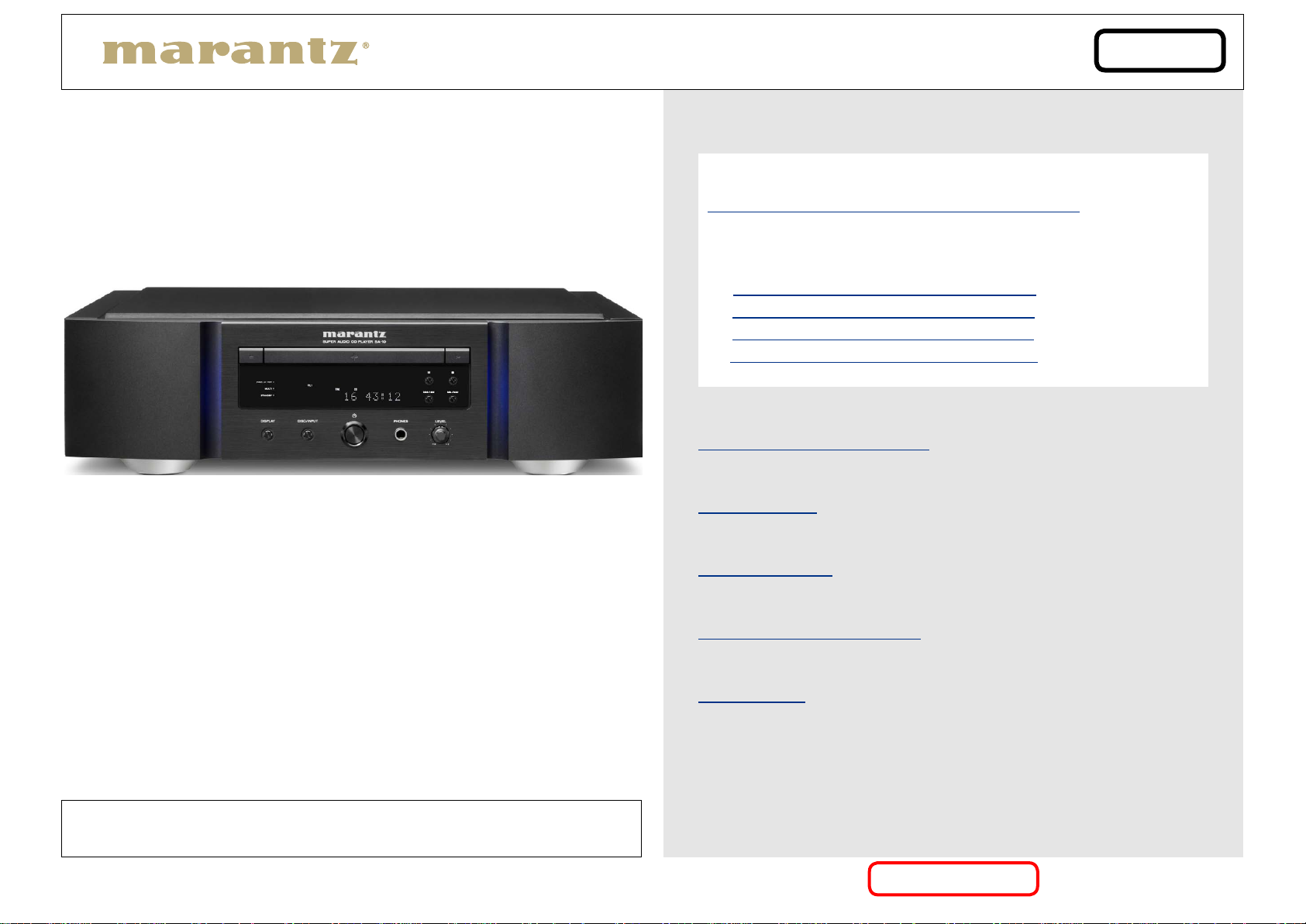
Super Audio CD Player
SA-10
Service Manual
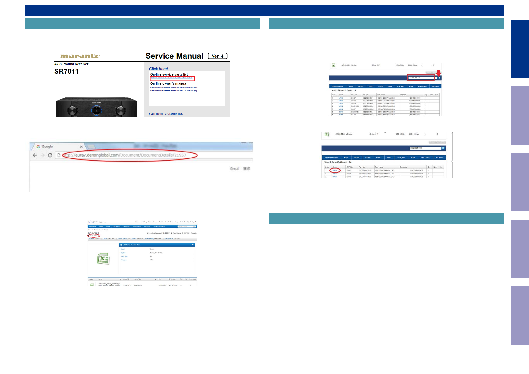
Click here!
On-line service parts list
http://dmedia.dmglobal.com/Document/DocumentDetails/23032
ONLINE PARTS LIST (P5)
WEB owner’s manual
NA: http://manuals.marantz.com/SA10/NA/EN/index.php
EU: http://manuals.marantz.com/SA10/EU/EN/index.php
AP: http://manuals.marantz.com/SA10/AP/ZH/index.php
JP: http://manuals.marantz.com/SA10S/JP/JA/index.php
CAUTION IN SERVICING
ELECTRICAL
Ver. 5
MECHANICAL
REPAIR INFORMATION
UPDATING
•Forpurposesofimprovement,specicationsanddesignaresubjecttochangewithoutnotice.
•Pleaseusethisservicemanualwhenreferringtotheoperatinginstructionswithoutfail.
•Someillustrationsusedinthisservicemanualareslightlydifferentfromtheactualproduct.
Please refer to the MODIFICATION NOTICE.
Condential
START::|UNA0JkWjR3Mx1oB5rVBS0Q==|1ASQkIk0vzO/wecjQ6R0ax1twb/Iubi+4qPfaYi43FQ=|lYV/KaXVYq6E/Xaks5O/YA==|::END
SAFETY PRECAUTIONS
NOTE FOR SCHEMATIC DIAGRAM
CAUTION IN SERVICING
Caution in
servicing
HANDLING THE SEMICONDUCTOR AND OPTICS
WARNING AND LASER SAFETY INSTRUCTIONS
ONLINE PARTS LIST
Accessing the Parts List
Searching Part Numbers or Ref. Numbers
NOTE FOR PARTS LIST
SERIAL NUMBER
Serial Number Organization
SKU Code of this Unit
CAUTION IN SERVICING.
Initializing This Unit
Electrical Mechanical Repair Information Updating
2
g
SAFETY PRECAUTIONS
The following items should be checked for continued protection of the customer and the service technician.
Leakage current check
Before returning the set to the customer, be sure to carry out either (1) a leakage current check or (2) a line to chassis resistance check. If the leakage current exceeds 0.5 milliamps, or if the resistance from chassis to either side of the power cord is less than 460 kohms, the set is defective.
Be sure to test for leakage current with the AC plug in both polarities, in addition, when the set's power is in each state (on, off and standby mode), if applicable.
Caution in
servicing
CAUTION
Please heed the following cautions and instructions during servic-
ing and inspection.
◎ Heed the cautions!
Cautions which are delicate in particular for servicing are labeled on the cabinets, the parts and the
chassis, etc. Be sure to heed these cautions and the cautions described in the handling instructions.
◎ Cautions concerning electric shock!
(1) An AC voltage is impressed on this set, so if you touch internal metal parts when the set is energized,
you may get an electric shock. Avoid getting an electric shock, by using an isolating transformer and
wearing gloves when servicing while the set is energized, or by unplugging the power cord when
replacing parts, for example.
(2) There are high voltage parts inside. Handle with extra care when the set is energized.
◎ Caution concerning disassembly and assembly!
Through great care is taken when parts were manufactured from sheet metal, there may be burrs on the
edges of parts. The burrs could cause injury if ngers are moved across them in some rare cases. Wear
gloves to protect your hands.
◎ Use only designated parts!
The set's parts have specic safety properties (re resistance, voltage resistance, etc.). Be sure to use
parts which have the same properties for replacement. The burrs have the same properties. In particular,
for the important safety parts that are indicated by the z mark on schematic diagrams and parts lists,
be sure to use the designated parts.
◎ Be sure to mount parts and arrange the wires as they were originally placed!
For safety seasons, some parts use tapes, tubes or other insulating materials, and some parts are mounted away from the surface of printed circuit boards. Care should also be taken with the positions of the
wires by arranging them and using clamps to keep them away from heating and high voltage parts, so
be sure to set everything back as it was originally placed.
◎ Make a safety check after servicing!
Check that all screws, parts and wires removed or disconnected when servicing have been put back
in their original positions, check that no serviced parts have deteriorated the area around. Then make
an insulation check on the external metal connectors and between the blades of the power plug. And
otherwise check that safety is ensured.
(Insulation check procedure)
Unplug the power cord from the power outlet, disconnect the antenna, plugs, etc., and on the power.
Using a 500V insulation resistance tester, check that the insulation resistance value between the inplug
and the externally exposed metal parts (antenna terminal, headphones terminal, input terminal, etc.) is
1M Ω or greater. If it is less, the set must be inspected and repaired.
CAUTION
Many of the electric and the structural parts used in the set have special safety properties. In most cases
these properties are difcult to distinguish by sight, and the use of replacement parts with higher ratings (rated power and withstand voltage) does not necessarily guarantee that safety performance will
be preserved. Parts with safety properties are indicated as shown below on the wiring diagrams and the
parts list in this service manual. Be sure to replace them with the parts which have the designated part
number.
(1) Schematic diagrams Indicated by the z mark.
(2) Parts lists Indicated by the z mark.
The use of parts other than the designated parts could cause electric shocks, res or other dangerous
situations.
Concerning important safety parts
Electrical Mechanical Repair Information Updating
3
g
NOTE FOR SCHEMATIC DIAGRAM
WARNING:
Parts indicated by the z mark have critical characteristics. Use ONLY replacement parts recommended
by the manufacturer.
CAUTION:
Before returning the set to the customer, be sure to carry out either (1) a leakage current check or (2)
a line to chassis resistance check. If the leakage current exceeds 0.5 milliamps, or if the resistance from
chassis to either side of the power cord is less than 460 kohms, the set is defective.
WARNING:
DO NOT return the set to the customer unless the problem is identied and remedied.
NOTICE:
(1) ALL RESISTANCE VALUES IN OHM. k=1,000 OHM / M=1,000,000 OHM
(2) ALL CAPACITANCE VALUES ARE EXPRESSED IN MICRO FARAD, UNLESS OTHERWISE INDICATED. P
INDICATES MICRO-MICRO FARAD. N INDICATES NANO FARAD.
(3) EACH VOLTAGE AND CURRENT ARE MEASURED AT NO SIGNAL INPUT CONDITION.
(4) CIRCUIT AND PARTS ARE SUBJECT TO CHANGE WITHOUT PRIOR NOTICE.
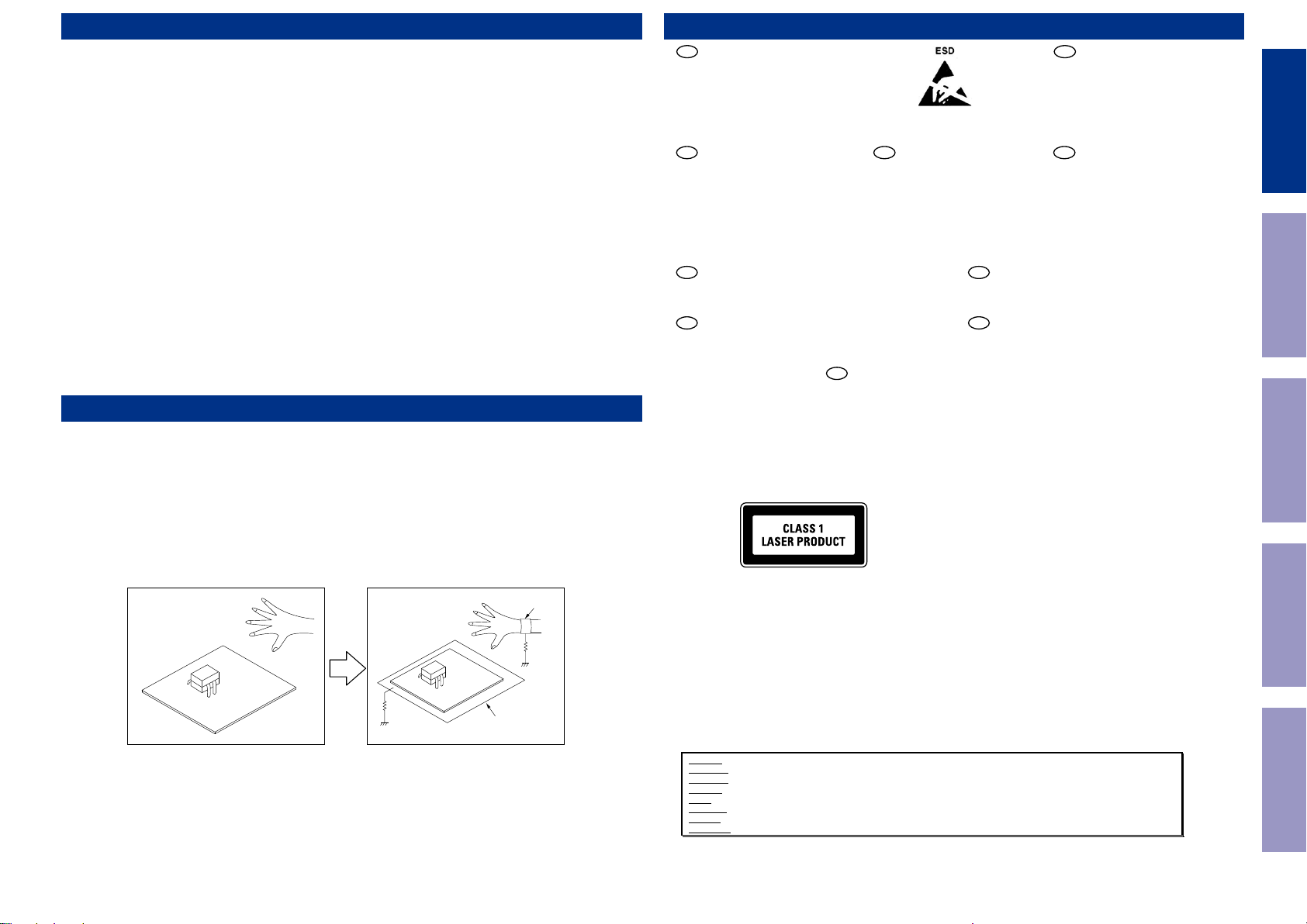
HANDLING THE SEMICONDUCTOR AND OPTICS
Electrostatic breakdown of the semi-conductors or optical pickup may occur due to a potential difference caused by electrostatic charge during unpacking or repair work.
1. Ground for Human Body
Be sure to wear a grounding band (1 M ohm) that is properly grounded to remove any static electricity
that may be charged on the body.
2. Ground for Workbench
Be sure to place a conductive sheet or copper plate with proper grounding (1 M ohm) on the workbench or other surface, where the semi-conductors are to be placed. Because the static electricity
charge on clothing will not escape through the body grounding band, be careful to avoid contacting
semi-conductors with your clothing
<Incorrect>
<Correct>
CBA
1MΩ
Grounding Band
CBA
Conductive Sheet or
Copper Plate
1MΩ
WARNING AND LASER SAFETY INSTRUCTIONS
WARNING
GB
All ICs and many other semi-conductors are
susceptible to electrostatic discharges (ESD).
Careless handling during repair can reduce life
drastically.
When repairing, make sure that you are connected
with the same potential as the mass of the set via a
wrist wrap with resistance.
Keep components and tools also at this potential.
F ATTENTION
Tous les IC et beaucoup d’autres semiconducteurs
sont sensibles aux décharges statiques (ESD).
Leur longévité pourrait être considérablement
écourtée par le fait qu’aucune précaution n’est prise
a leur manipulation.
Lors de réparations, s’assurer de bien être relié au
même potentiel que la masse de l’appareil et enfiler
le bracelet serti d’une résistance de sécurité.
Veiller a ce que les composants ainsi que les outils
que l’on utilise soient également a ce potentiel.
GB
Safety regulations require that the set be restored to its original condition
and that parts which are identical with those specified be used.
NL
Veiligheidsbepalingen vereisen, dat het apparaat in zijn oorspronkelijke
toestand wordt terug gebracht en dat onderdelen, identiek aan de
gespecifieerde worden toegepast.
“Pour votre sécurité, ces documents
doivent être utilisés par des
spécialistes agrées, seuls habilités à
réparer votre appareil en panne.”
F
Les normes de sécurité exigent que l’appareil soit remis a l’état d’origine et
que soient utilisées les pièces de rechange identiques à celles spécifiées.
D
WARNUNG
Alle IC und viele andere Halbleiter sind
empfindlich gegen elektrostatische
Entladungen (ESD).
Unsorgfältige Behandlung bei der Reparatur
kann die Lebensdauer drastisch vermindern.
Sorgen sie dafür, das Sie im Reparaturfall
dem Massepotential des Gerätes verbunden
sind.
Halten Sie Bauteile und Hilfsmittel ebenfalls
über ein Pulsarmband mit Widerstand mit auf
diesem Potential.
D
Bei jeder Reparatur sind die geltenden Sicherheitsvorschriften zu beachten.
Der Originalzustand des Gerats darf nicht verandert werden.
Fur Reparaturen sind Original-Ersatzteile zu verwenden.
I
Le norme di sicurezza esigono che l’apparecchio venga rimesso nelle
condizioni originali e che siano utilizzati pezzi di ricambiago idetici a quelli
specificati.
LASER SAFETY
This unit employs a laser. Only a qualified service person should
remove the cover or attempt to service this device, due to
possible eye injury.
USE OF CONTROLS OR ADJUSTMENTS OR PERFORMANCE
OF PROCEDURE OTHER THAN THOSE SPECIFIED HEREIN
MAY RESULT IN HAZARDOUS RADIATION EXPOSURE.
AVOID DIRECT EXPOSURE TO BEAM
WARNING
The use of optical instruments with this product will
increase eye hazard.
Repair handling should take place as much as possible with
a disc loaded inside the player
WARNING LOCATION: INSIDE ON LASER COVERSHIELD
CAUTION VISIBLE AND INVISIBLE LASER RADIATION WHEN OPEN AVOID EXPOSURE TO BEAM
ADVARSEL SYNLIG OG USYNLIG LASERSTRÅLING VED ÅBNING UNDGÅ UDS
ADVARSEL SYNLIG OG USYNLIG LASERSTRÅLING NÅR DEKSEL Å PNES UNNGÅ EKSPONERING FOR STRÅLEN
VARNING SYNLIG OCH OSYNLIG LASERSTRÅLNING NÄR DENNA DEL ÄR ÖPPNAD BETRAKTA EJ STRÅLEN
VARO! AVATT AESSA OLET ALTTIINA NÄKYVÄLLE JA NÄKYMÄTTÖMÄLLE LASER SÄTEILYLLE. ÄLÄ KATSO SÄTEESEEN
VORSICHT SICHTBARE UND UNSICHTBARE LASERSTRAHLUNG WENN ABDECKUNG GEÖFFNET NICHT DEM STRAHL AUSSETSEN
DANGER VISIBLE AND INVISIBLE LASER RADIATION WHEN OPEN AVOID DIRECT EXPOSURE TO BEAM
ATTENTION RAYONNEMENT LASER VISIBLE ET INVISIBLE EN CAS D'OUVERTURE EXPOSITION DANGEREUSE AU FAISCEAU
Æ
TTELSE FOR STRÅLING
WAARSCHUWING
NL
Alle IC’s en vele andere halfgeleiders zijn gevoelig
voor elektrostatische ontladingen (ESD).
Onzorgvuldig behandelen tijdens reparatie kan de
levensduur drastisch doen verminderen.
Zorg ervoor dat u tijdens reparatie via een polsband
met weerstand verbonden bent met apparaat.
Houd componenten en hulpmiddelen ook op
ditzelfde potentiaal.
I
AVVERTIMENTO
Tutti IC e parecchi semi-conduttori sono sensibili
alle scariche statiche (ESD).
La loro longevita potrebbe essere fortemente ridatta
in caso di non osservazione della piu grande
cauzione alla loro manipolazione.
Durante le riparazioni occorre quindi essere
collegato allo stesso potenziale che quello della
massa dell’apparecchio tramite un braccialetto a
resistenza.
Assicurarsi che i componenti e anche gli utensili
con quali si lavora siano anche a questo potenziale.
100301DM
Caution in
servicing
Electrical Mechanical Repair Information Updating
4
g
ONLINE PARTS LIST
Accessing the Parts List
(1) Access from the Service Manual
・ Click the URL link on the cover of the service manual.
Examples of display
NOTE : If the web browser does not open automatically, copy the URL and paste it into the address bar
of the web browser and then press Enter.
(2) Accessing the Part List from the Model Asset Screen.
・ Display Model Asset from New SDI.
・ Click the section displayed as ▼ Link to Part Lists under the model name.
Searching Part Numbers or Ref. Numbers
You can search a Parts List for part numbers or Ref. numbers.
(1) Enter the part number or Ref. number in the search window of the Parts List, and press the search
button.
(2) The search results are displayed.
The name of the sheet in which the search part is used and the part’s line are displayed.
(3) Next, click the "Sheet" section of the search results.
NOTE FOR PARTS LIST
1. Parts indicated by "
2. When ordering a part, make a clear distinction between "1" and "I" (i) to avoid mis-supplying.
3. A part ordered without specifying its part number can not be supplied.
4. Part indicated by "@" mark is not illustrated in the exploded and packaging view.
WARNING: Parts indicated by the z mark have critical characteristics. Use ONLY replacement parts
recommended by the manufacturer.
nsp
" on this table cannot be supplied.
Caution in
servicing
Electrical Mechanical Repair Information Updating
NOTE : If the ▼ Link to Parts List section is not displayed, download the parts table from the Asset list.
5
g
SERIAL NUMBER
Serial Number Organization
The 14-digit serial number that contains the code of the manufacturing plant and the manufacturing
date.
14 digits
Caution in
servicing
SKU
code
Factory
code
The last
2digit of year
SKU Code of this Unit
Product SKU SKU Code
SA10S1/U1B
SA10S1/U1G
SA10S1/N1B
SA10S1/N1G
SA10S1/K1G
SA10S1/FN
Manufactured
Year, month
Month
(01 ~ 12)
Cumulative
serial number
ANR
AQK
ANP
ANQ
ANN
ANM
Electrical Mechanical Repair Information Updating
6
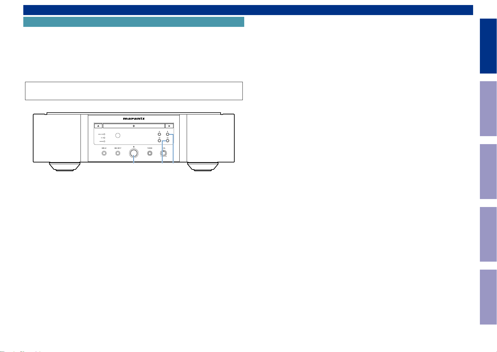
CAUTION IN SERVICING.
Initializing This Unit
Make sure to initialize this unit after replacing the microcomputer or any peripheral equipment, or the
CD PCB.
Caution in
servicing
1. Press the power button to turn off the power.
2. While holding down buttons "
the power.
INITIALIZED
3. "
4. After 10 seconds, switch to the normal mode.
NOTE: • If the unit fails to enter the service mode in step 3, repeat the procedure from step 1.
" is displayed.
• Initializing the device restores the customized settings to the factory settings. Write down
your settings in advance and recongure the settings after initialization.
STOP
" and "9" simultaneously, press the power button to turn on
X
92
Electrical Mechanical Repair Information Updating
7
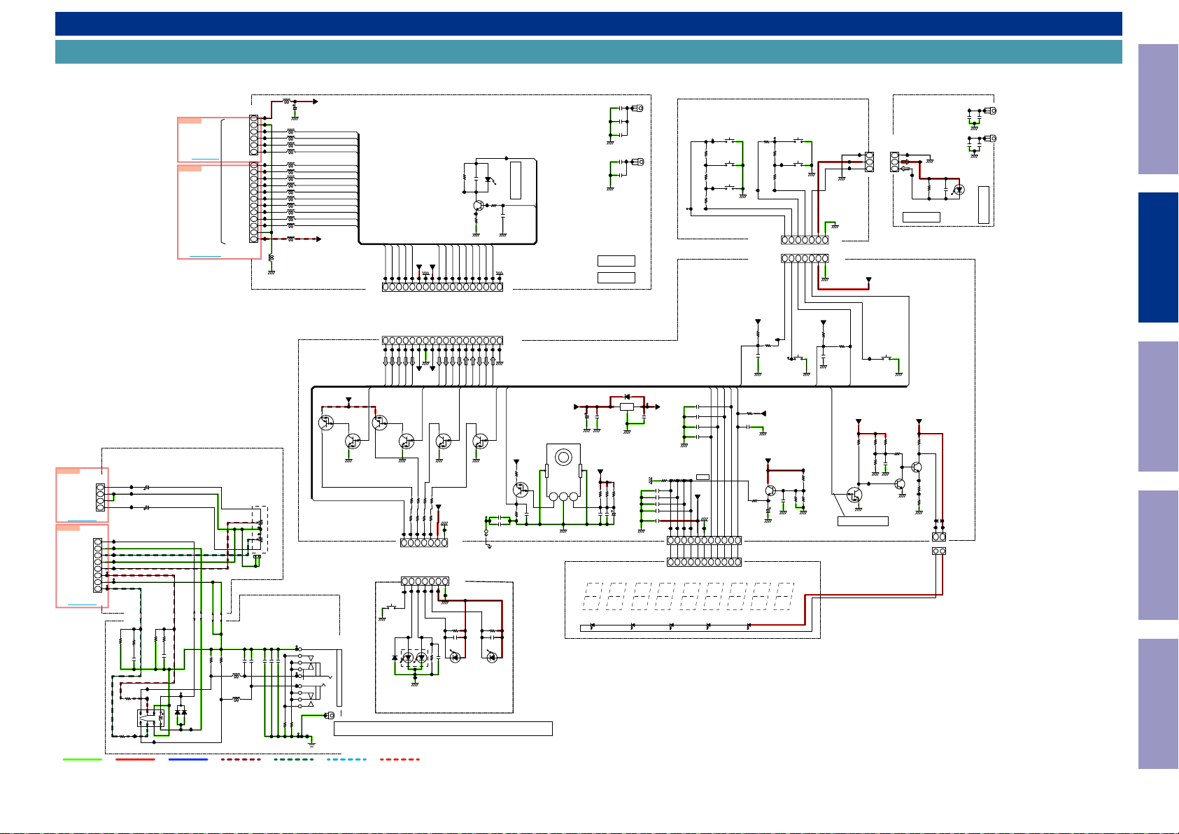
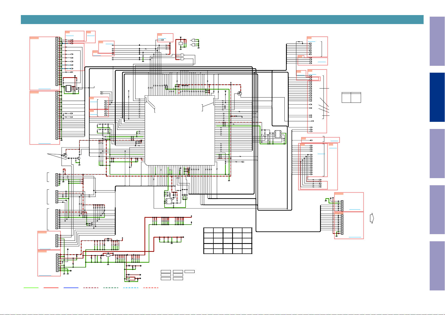
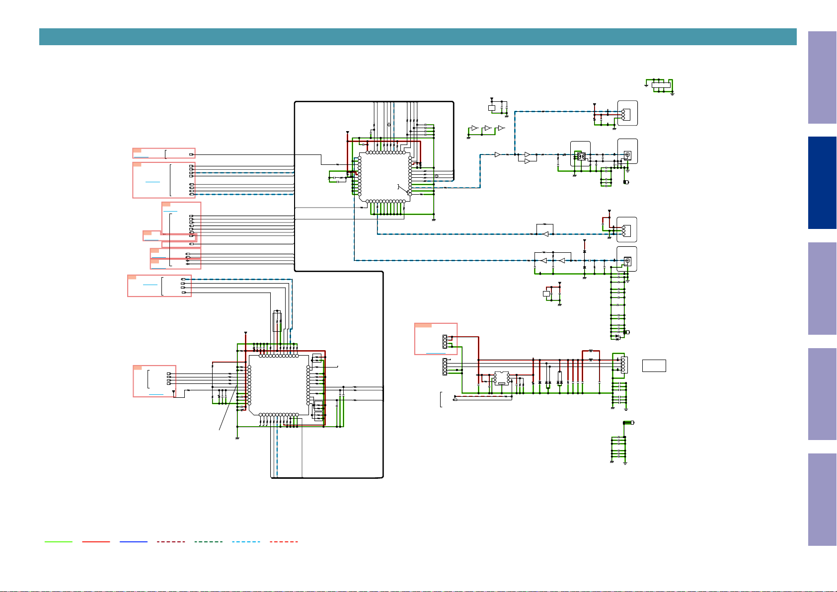
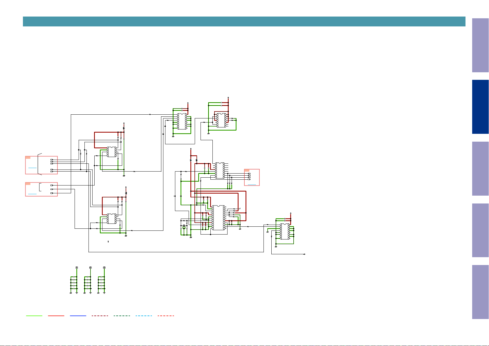
SCHEMATIC DIAGRAMS
ELECTRICAL
PRINTED CIRCUIT BOARDS
Caution in
servicing
SCH01_FRONT
SCH02_D.POWER(1/2)
SCH03_D.POWER(2/2)
SCH04_HP AMP
SCH05_DIGITAL(1/7)
SCH06_DIGITAL(2/7)
SCH07_DIGITAL(3/7)
SCH08_DIGITAL(4/7)
SCH09_DIGITAL(5/7)
SCH10_DIGITAL(6/7)
SCH11_DIGITAL(7/7)
SCH12_AUDIO(1/4)
SCH13_AUDIO(2/4)
SCH14_AUDIO(3/4)
SCH15_AUDIO(4/4)
SCH16_MECHA(1/4)
SCH17_MECHA(2/4)
SCH18_MECHA(3/4)
SCH19_MECHA(4/4)
DIGITAL, D.POWER
AUDIO
FRONT CENTER, P.SW, LED, LEFT SLED, RIGHT SLED, HP AMP, T.SW, VR_HP JACK,
MECHA
BLOCK DIAGRAM
POWER DIAGRAM
WIRING DIAGRAM
SEMICONDUCTORS
1. IC's
2. FL DISPLAY
Electrical Mechanical Repair Information Updating
8
SCHEMATIC DIAGRAMS
SCH01_FRONT
N601
6P-PHs
1
+12VF
GND
F_RS
FCEN
FCLK
FDAT
FRES
LCDOFF
RC5F
S_OFF
MULTI
D_OFF
LED_GREEN
LED_RED
AUDIO UNIT
(L-1)
KEY1
KEY0
GND
+3.3ST
N1201
12P-PHs
SHORT
SHORT
SHORT
SHORT
J6504
J6503
J6506
J6505
C6520 1000P
47K
47K
R6564
R6565
L6503
BLM21PG221
L6504
BLM21PG221
1SS301
D6507
ANALOG AUDIO R ANALOG AUDIO L
2
3
4
5
6
1
2
3
4
5
6
7
8
9
10
11
12
3
6
8
8U-210221-9
HP JACK UNIT
1000P
C6521
N412
TO N402
N812
PHR-SAN_8P
M_RELAY
GND
L_VOLOUT
GND
R_VOLOUT
R_HPAOUT
H.GND
L_HPAOUT
TO N802
GND LINE
N412
4P-PH
RIN
GND
GND
LIN
1
2
3
4
N812
1
2
3
4
5
6
7
8
VR UNIT
8U-210221-8
C7802
47/25
C7702
47/25
HPGND1.
HPGND2.
J6501
SHORT
R6556
R6554
R6555
22(1W)
5.6K
0.039
C6518
1
R6558
234
S6501
R6559
1
81765
G6K-2P-Y
POWER+ LINE
J6502
SHORT
R6557
5.6K
22(1W)
C6519
0.039
POWER- LINE
N601
TO N611
N1201
TO N1211
1
2
3
2
1
4
5
L5301
7
+12VF0
BLM21PG221
L5313
L5312
L5311
L5310
L5309
L5308
L5307
L5306
L5305
L5315
L5317
L5304
L5303
L5302
L5316
BLM21PG221
GNDF1.
V3501
A10K
0.1
1000P
C6523
C6522
L5314
0.01
C6524
0
R6580
C5301
10/35
GNDF1.
BLM18HG102SN1D
BLM18HG102SN1D
BLM18HG102SN1D
BLM18HG102SN1D
BLM18HG102SN1D
BLM18HG102SN1D
BLM18HG102SN1D
BLM18HG102SN1D
BLM18HG102SN1D
BLM18HG102SN1D
BLM18HG102SN1D
BLM18HG102SN1D
BLM18HG102SN1D
BLM18HG102SN1D
BLM21PG221
1
6
5
4
3
2
7
8
9
0
R6581
OP/CL
FG1
1P_L=100_SRA3-SIN1.8
FG1
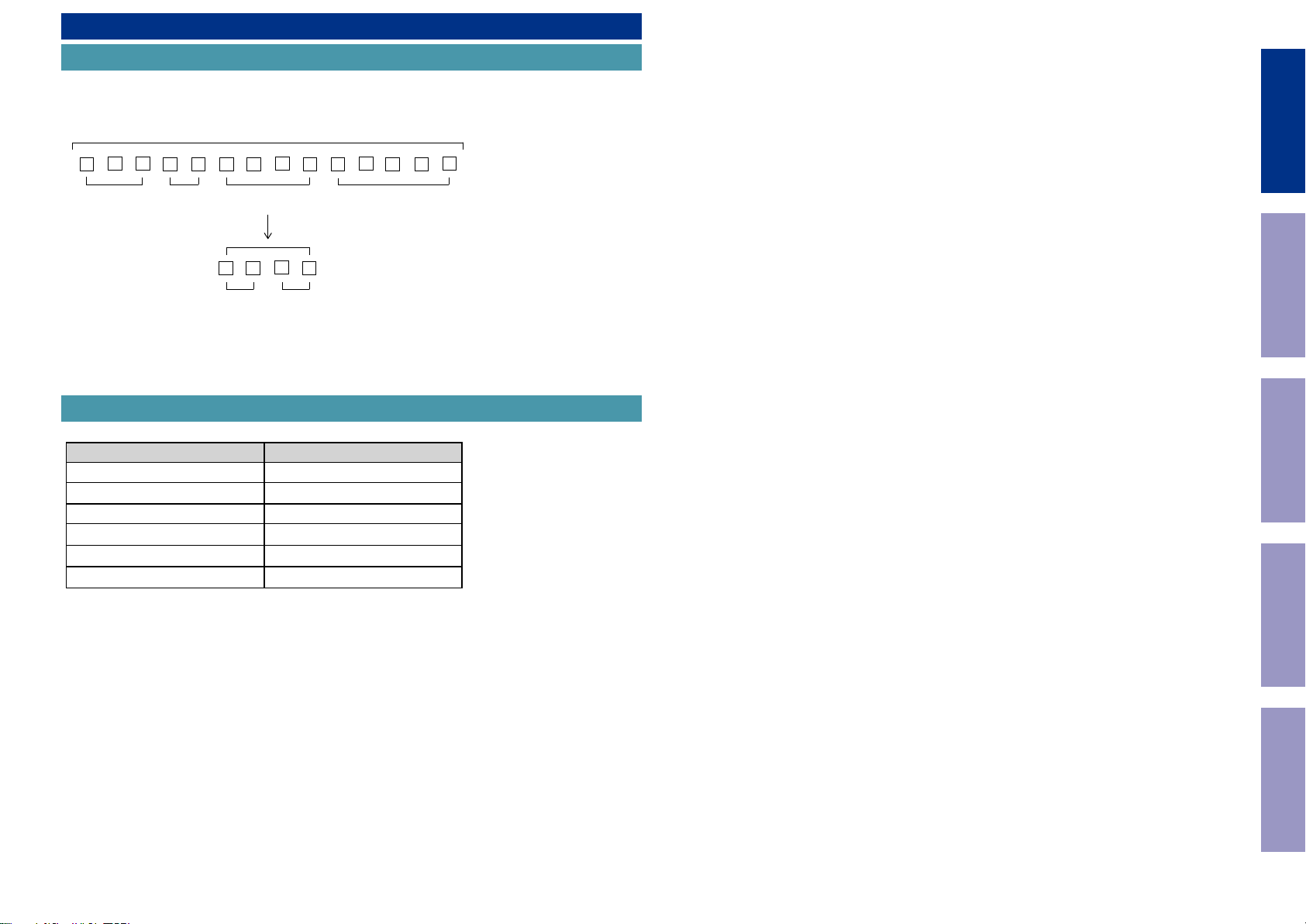
All Ref.No. has been described in the parts list are four digits.
But there are less than four digits of printed Ref.No. on the PCB, and they have become four digits after the header by adding "0" in the parts list.
+12VF1
G : PHONE JACK BOARD(9P)
B : H7098F120N
B6501
8U-210221-3
LEFT SLED UNIT
F_RS.
FCEN.
+3.3ST1.
DTA114EEB
K6501
FCLK.
FDAT.
FRES.
LCDOFF.
RC5F.
S_OFF
MULTI.
D_OFF.
LED_GREEN.
LED_RED.
+3.3ST2
Q5010
GNDF2
Z3301
KEY1.
KEY0.
GND-TERMINAL
Q5009
N1903
LED_RED
KRC402E-RTK
FDAT.
FCLK.
1
2345678
18P-FFCs
FCLK
FDAT
17
18
FDAT
FCLK
Q5011
DTA114EEB
S5305
SKHVBF
OP/CL
GNDF4
D5104
KDS160
SML-022ML8T
FCEN.
FCEN
16
FCEN
GNDF2
D5101
F_RS.
FRES.
F_RS
15
F_RS
FRES
330
R5028
0
R5029
7
LED_RED
OP/CL
7
3.3ST
STAND BY
(RED)
+12VF1
FRES
+12VF
13
14
+12VF2
LED_GREEN
Q5001
KRC402E-RTK
220
R5001
0
R5031
R5030
6
5
LED_GREEN
5
6
GNDF4
390
R5002
0
4
M-CH2
2SC4081
MULTI.
D_OFF.
+3.3ST1.
LED_GREEN.
GNDF1.
11
9
10
GND
M-CH
D_OFF
+3.3ST1
LED_GREEN
11
8
9
10
12
GNDF2
M-CH
+3.3ST2
LED_GREEN
D_OFF
Q5002
GNDF2
3.9K
+12VF2
R5003
0
GNDF2
R5032
1
3
2
GND
+12FV
D_OFF2
1
2
3
4
GNDF4
R5101
10K
3.3ST
C5101
0.1
0.1
10K
C5102
D5102
R5102
SML310BAT-T86
MULTI CH
(BLU)
8U-210221-5
FRONT SIDE LED
LED_SPACER(45151022600AS)が必要です
(RIGHT)
0.1
10K
R5301
D5301
C5302
Q5301
150
R5302
GNDF1.
KEY1.
KEY0.
S_LED.
LCDOFF.
LED_RED.
12131415161718
KEY1
KEY0
LED_RED
LCDOFF
4
5
6
7
LED_RED
S_LED
LCDOFF
KEY0
KEY1
M-CH
KRC402E-RTK
GNDF2
B5506
OPEN
-
N701
7P-FFCs
N711
7P-FFC
12V
DISPLAY OFF
LED UNIT
R5303
2.2K
RC5F.
RC5F
S_LED
2
3
RC5F
D_OFF
Q5003
KRC402E-RTK
C5021
C5022
EARTH
R5103
10K
C5103
0.1
D5103
SML-E12V8W
(RED)
TOL-306UBFC
GNDF1.
GNDF1.
GND
1
GNDF2
RC5F
OPEN
OPEN
Headphone amplifier output impedance : 11ohm
DIGITAL AUDIO
STBY POWER
Z5301
0.1
C5303
GND
18P-FFC
+3.3ST2
R5005
12V
S_LED.
LED_SPACER
S_OFF
N1913
R5004
100
47K
8U-210221-2
FRONT CENTER UNIT
U5002
NJM2845DL1-33
+12VF2
C5003
100/16
U5001
GNDF2
GNDF2
GNDF2
+3.3ST2
GND3VCC1VOUT
100
R5006
2
C5002
0.1
R34ES9A-15MM(36KHZ)
Q5004
DTA114EEB
C5001
100P
LCD DISPLAY ASSY
D001
GNDF1.
GNDF1.
C5005
100
R5007
STYLE-PIN
STYLE-PIN
非標準部品
0.1
C5004
C5305
1000P
C5306
1000P
C5309
1000P
GND-TERMINAL(OPEN)
C5310
1000P
C5311
1000P
Z5303
Z5302
D5105
IN
GNDF2
R5008
100
C5006
47/6.3
0.47
B5203
OPEN
B5204
KDS160
OUT
D002
GNDF2
GNDF2
Caution in
servicing
B5201
8U-210221-6
T.SW UNIT
S5301
SKHVBF
PLAY
S5302
150
R5306
TACT
STOP
S5303
180
R5307
TACT
PAUSE
GNDF2.
270
R5308
+3.3ST2
KEY1
FRES
FCEN
FCLK
FDAT
C5012
+3.3VF2
C5013
C5023
OPEN
C5014
C5015
GNDF2
1K
1K
R5009
R5010
R5011
1K
C5008
0.47
0.47
C5009
C5010
0.47
C5011
0.47
C5007
0.1
XV
XV
XV
1
2345678
-
1
2345678
F_RS
1000P
1000P
1000P
1000P
1K
R5012
6.2V
+3.3VF2
3.3V
XV
GNDF2
R5013
22K
C5016
0.1
XV
XV
9
11
10
9
11
10
Z5003
OPEN
R5014
N5005
11P-FFCs
GNDF2
0
GNDF2
R5311
+12VF2
C5017
150
R5304
R5305
C5304
2.2/50
GNDF2
180
R5312
270
R5313
N702
N712
OPEN
0
0.1
+3.3VF2
2SC4081
7
7P-FFCs
1
7P-FFCs
12V
Q5005
6.8V
0.47
C5018
GNDF2
TACT
NEXT
TACT
PREV
SKHVBF
R5015
S5306
S5307
6
2
S5304
DIMMER
6.8K
5
GNDF2
GNDF2.
GNDF2.
GNDF2.
1
4
3
2
3
4
5
6
7
GNDF2
+3.3ST2
R5309
OPEN
R5310
0
0.1
C5312
GNDF2
GNDF2
KEY0
OP/CL
LCDOFF
+3.3VF2
R5018
3.9K
R5016
47K
Q5006
R5017
KRC402E-RTK
00MBA2000399Y
GNDF2
H ; LCD BACK LIGHT ON
8U-210221-4
RIGHT SLED UNIT
N311
3P-PHs
GND
1
1
+12V
2
2
GNDF3
3
Z5203
STYLE-PIN
10K
R5205
FRONT SIDE LED
0.1
C5201
+12VF2
3
3P-PHs
N301
S_LED
S5308
SKHVBF
DISC/INPUT
GNDF2
S_LED
LCD BACK LIGHT LED CKT
+12VF2
R5021
R5023
680
1K
560
GNDF2
R5019
R5020
1.8K
GNDF2
Q5007
2SC4081
10K
R5022
1K
C5019
0.1
Q5008
2SC4081
47
R5024
GNDF2
R5025
470
GNDF2
1
2
OPEN
OPEN
C5204
OPEN
C5203
GNDF3
B5202
GND-TERMINAL(OPEN)
OPEN
C5206
OPEN
C5205
GNDF3
(LEFT)
D5201
TOL-306UBFC
Z5211
LED_SPACER
C5020
0.1
N5004
2P-PHs
Electrical Mechanical Repair Information Updating
LCD DISPLAY LED WIRE
D003
D004
D005
9
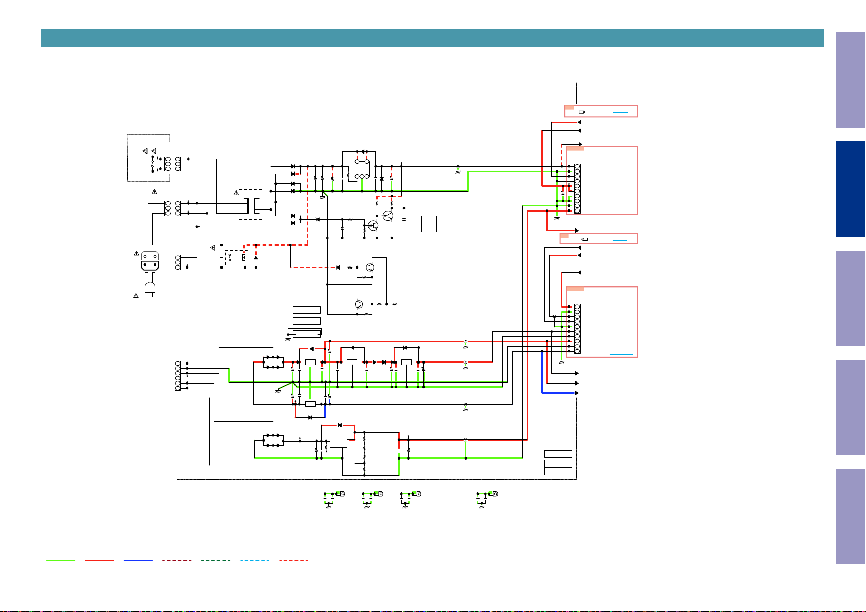
SCH02_D.POWER(1/2)
All Ref.No. has been described in the parts list are four digits.
But there are less than four digits of printed Ref.No. on the PCB, and they have become four digits after the header by adding "0" in the parts list.
Caution in
servicing
8U-210221-7
POWER SW UNIT
C8001
1 2
470P/250V
S8001
66105000300AS
POWER-SWITCH(TV-5)
7.92MM-PITCH-BASE-2PIN(TOP)
12
1 2
1
2
Z8001
AC-CORD
N8001
2P-VHws
L003
W8001
Z8002
N8002
2P-VHw
1
1
2
2
N8003
2P-VHw
2
2
1
1
2
1
N8006
6P-VH
1
2
3
4
5
6
8U-210221-1(1/2)
C8002
470P/250V
RELAY_DLS1U
S8002
N8004
2P-VHw
T8001
U : SUB TRANS (U) A363
N, K : SUB TRANS (N) A363
F : SUB TRANS (F) A363
T8001
91
8
2
7
3
6
4
5
10101014400AM
34
1
2
D8012
11EQS10
D8001
1SS355T
D8013
11EQS10
D8014
11EQS10
D8015
11EQS10
D8003
RSX101M-30
D8006
RSX101M-30
D8007
RSX101M-30
D8016
11EQS10
D8017
11EQS10
GND
D8018
11EQS10
D8019
11EQS10
D8002
RSX101M-30
D8004
1SR154
D8005
1SR154
Z8005
TR_SHIELD
Z8003
SCREW
00M51100308M9
44741010900AS
HEAT-SINK_W26.2xL30
GND
D8022
NJM7812FA
φ18
IN
C8009
4700/35
C8010
4700/35
NJM7912FA
D8023
Z8004
U8002
C8011
C8012
IN
U8003
C8027
1000/16
D8008
UDZS3.6B
KDS160
OUT
C8015
OPEN
OPEN
KDS160
C8013
2200/25
GND
OPEN
C8016
OUT
C8081
C8003
+12V
C8014
1000/16
47K
R8001
C8005
2.2/50
D8009
UDZS11B
C8019
OPEN
D8026
U8004
NJM2387DL3
1
Vin
CONT
2
R8012
4.7K
OPEN
GND-TERMINAL(OPEN)
OPEN
GND
C8017
0.1
C8018
B8001
C8082
470/16
220/25
0.022C8004
NJM2831F33
R8003
12K
R8002
D8024
NJM7809FA
IN
KDS160
3
Vout
Vadj
4
GND
5
非標準部品
OPEN
D8010
10K
R8004
U8001
2.7K
Q8002
U8005
5
IN
1CT2
R8006
R8005
8.2K
2SC4081
KDS160
OUT
R8016
1K
C8083
GND3NC
4.7K
R8007
10K
C8022
OPEN
1SS355T
4
OUT
C8006
R8008
Q8003
KRC111S
D8020
1SR154
0.1
R8013
8.2K
R8014
220
100
R8015
GND-TERMINAL(OPEN)
GND
0.022
10K
R8009
1K
B8002
C8084
Q8001
OPEN
D8021
1SR154
1SR154
D8011
R8010
2SC4081
3.3K
C8023
470/16
C8007
Q8004
10K
KRC111S
使用不可
R8011
D8025
NJM7805FA
IN
C8020
OPEN
C8085
470/16
U8006
C8024
OPEN
GND
C8008
0.1
KDS160
OUT
OPEN
C8025
B8003
GND-TERMINAL(OPEN)
C8086
OPEN
C8021
470/16
OPEN
TO
L8021
C8302
C8605
C8026
470/16
L8001
NFM18PS105R0J3
GND
L8002
NFM2012P13C105F
GND
L8003
NFM18PS105R0J3
GND
L8004
NFM2012P13C105F
GND
L8005
NFM2012P13C105F
A0
BIDIRECT
+5V_D
N1002
N1002
PHR-SAN_10P
1
2
3
4
5
6
7
C8028
100/10
8
9
10
GND
+12V_LCD
A1
BIDIRECT
+6V_M
N1001
N1001
10P-PH
1
L8006
2
NFM2012P13C105F
3
4
5
6
7
8
9
10
GND
+5M
+12M
-12M
Z5204
STYLE-PIN
Z5202
OPEN
Z5201
STYLE-PIN
B8081
GND-TERMINAL(OPEN)
OPEN
C8089
OPEN
C8090
GND
P_DOWN
+5V_DSP
+3.3V_NSW
+3.3V_NSW
GND
+5V_D
GND
+5V_DSP
+5V_DSP
GND
GND
GND_LCD
+12V_LCD
M_TRANS_ON
+3.3V_M
VBUS_5V
VBUS_5V
VBUS_GND
+6V_M
+3.3V_M
GND
+5M
GND_M
+12M
GND_M
-12M
TO 0A
to DIGITAL UNIT
TO N1012
TO 1A
to MECHA UNIT
TO N1011
Electrical Mechanical Repair Information Updating
GND LINE
POWER+ LINE
POWER- LINE
ANALOG AUDIO R ANALOG AUDIO L
DIGITAL AUDIO
STBY POWER
10
SCH03_D.POWER(2/2)
All Ref.No. has been described in the parts list are four digits.
But there are less than four digits of printed Ref.No. on the PCB, and they have become four digits after the header by adding "0" in the parts list.
Caution in
servicing
8U-210221-1(2/2)
N8101
5P-VH
1
2
3
4
5
N8102
2P-VHw
1
2
Q8103
R8118
KTC3875S
22K
10K
R8117
Q8104
KTC3875S
GND
T3.15A_250V
F8101
T3.15A_250V
F8201
R8119
4.7K
R8122
4.7K
Q8105
KTA1504S
R8121
22K
10K
R8120
+3.3V_NSW
R8123
Q8106
KTA1504S
VBUS_ON
4.7K
10K
R8124
4.7K
Q8107
VBUS_5V
R8125
KTC3875S
Z8102
SCREW
00M51100308M9
Z8101
RADIATOR
00D4170669005
Z8203
SCREW
00M51100308M9
Z8202
RADIATOR
00D4170669005
KTC3875S
D8109
R8126
R8127
Q8108
UDZS5.1B
1K
10K
R8129
22K
Q8109
10K
R8128
KTC3875S
D8101
D3SB60
D8103
11EQS10
D8104
11EQS10
D8202
D3SB60
R8130
Q8110
KTA1504S
R8132
4.7K
R8133
4.7K
22K
10K
R8131
D8105
11EQS10
D8106
11EQS10
Q8111
KTA1504S
6800/16
C8101
GND
C8107
3300/16
6800/16
C8202
GND
VOLTAGE PROTECT
4.7K
R8134
10K
R8135
R8136
Q8112
KTC3875S
0.1
6800/16
C8103
C8119
C8108
OPEN
6800/16
C8204
0.1
C8218
M_TRANS_ON
+5V_D
D8110
UDZS6.8B
R8137
4.7K
R8138
GND
N314
3P-PH
2345 1
N714
7P-PH
BIDIRECT
BIDIRECT
1
2
3
4
1
2
3
4
5
6
8
1
2
3
4
5
6
7
C8227
33/16
VBUS_5V
TO N401
+5V_VBUS
+5V_VBUS
GND_VBUS
GND_VBUS
TO N304
+4V_USB
GND_USB
GND_USB
EXT
INT
K8101
RCA206B02
RC5S
TO N703
RC5F
GND
M_TRANS_ON
VBUS_ON
VOLTAGE_PROTECT
P_DOWN
P_DOWN
M_TRANS_ON
+6V_M
+5V_D
+3.3V_M
+5V_DSP
RC-5
INT/EXT SW
RC-5
IN OUT
TO A0
TO A1
Electrical Mechanical Repair Information Updating
C8109
C8111
L8102
NFM2012P13C105F
+6V_M
D8111
KDS160
U8206
BA00JC5WT
2
IN
R8212
CTL
1
GND
4.7K
C8106
1000/35
C8116
1000/35
C8105
1000/35
3
D8112
U8106
BA00JC5WT
2
IN
R8112
CTL
1
GND
4.7K
3
D8116
U8104
BA00JC5WT
2
IN
R8101
CTL
1
GND
4.7K
3
C8104
0.1
0.1
0.1
OUT
C
5
KDS160
OUT
C
5
KDS160
OUT
C
5
5
4
R8215
130K
R8213
12K
C8110
C8220
2200/16
0.1
R8214
47K
+3.3
4
R8115
56K
R8113
22K
R8114
47K
+5VDSP
4
R8107
130K
R8104
12K
R8105
47K
C8120
2200/16
C8113
2200/16
0.1
C8114
C8117
GND
0.1
GND
GND
HEAT-SINK_W26.2xL30
HEAT-SINK_W26.2xL30
HEAT-SINK_W26.2xL30
Z8211
44741010900AS
Z8213
TR_SHIELD
Z8111
44741010900AS
Z8113
TR_SHIELD
Z8104
44741010900AS
Z8106
TR_SHIELD
Z8212
SCREW
00M51100308M9
Z8112
SCREW
00M51100308M9
Z8107
SCREW
00M51100308M9
+4V_USB
GND_USB
GND
GND
L8106
NFM18PS105R0J3
GND
GND
L8206
NFM18PS105R0J3
L8201
NFM18PS105R0J3
L8107
NFM18PS105R0J3
+5V_D
Q8101
KRA102S
(10K-10K)
Q8102
KRC111S
GND
D8117
KDS160
U8103
BA00JC5WT
2
IN
4
OUT
CTL
1
R8106
130K
GND
C
3
5
R8102
C8115
0.1
18K
C8112
2200/16
R8108
470
R8103
47K
GND
Z8105
HEAT-SINK
44731006900AS
Z8109
TR_SHIELD
Z8108
SCREW
00M51100308M9
L8103
NFM18PS105R0J3
GND
L8104
NFM18PS105R0J3
GND
+5V_VBUS
C8225
D8107
1SS355T
RC5F
1uH
L8207
C8226
0.1
0.1
C8223
470/16
0.1
C8224
GND
N411
N411
4P-PH
GND
N314
S8101
JSS2208A
1
2
3
0.1
C8122
47
R8116
GND
N714
OPEN
C8123
GND
GND
0.01
C8126
GND
7
1000P
C8125
GND
0A
RC5S
D8108
1SS355T
C8121
470P
GND GND
1A
+12V_LCD
+3.3V_M
+5V_DSP
+5M
+12M
D8113
UDZS13B
非標準部品
1K
R8149
R8150
10K
KTA1504S
Q8119
R8151
2.2K
R8152
Q8120
KTC3875S
R8218
R8219
4.7K
R8155
D8115
UDZS5.1B
Q8121
330
KTA1504S
330
R8156
Q8122
10K
KTC3875S
R8157
R8158
330
KTC3875S
330
Q8123
Q8124
KTC3875S
1u
C8124
R8160
1K
OPEN
R8159
-12M
R8161
R8162
10K
10K
10K
D8114
UDZS3.6B
330
R8153
10K
R8154
330
Q8125
KTA1504S
R8216
R8217
Q8126
4.7K
KTC3875S
D8203
UDZS5.1B
R8147
22K
KTA1504S
330
330
Q8117
R8148
Q8118
4.7K
KTC3875S
GND LINE
POWER+ LINE
POWER- LINE
ANALOG AUDIO R ANALOG AUDIO L
DIGITAL AUDIO
STBY POWER
11
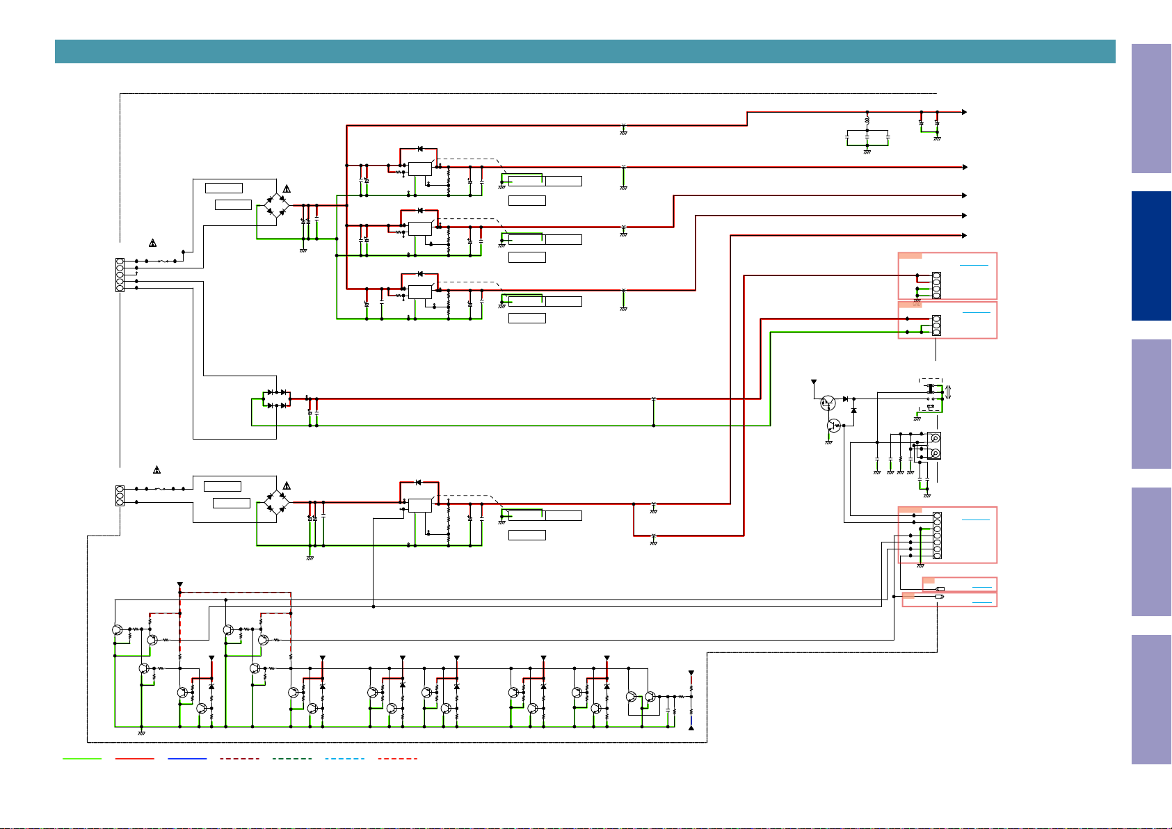
SCH04_HP AMP
N713
M_RELAY
relay_GND
gain_H
gain_M
+18V
AGND
-18V
TO N703
HP AMP PWB
N713
7P-PH
1
2
3
4
5
6
R6501
7
OPEN
C6502
220/35
C6503
220/35
+18V..
-18V..
C6504
47/25
HPGND
C6505
47/25
All Ref.No. has been described in the parts list are four digits.
But there are less than four digits of printed Ref.No. on the PCB, and they have become four digits after the header by adding "0" in the parts list.
Z6007
TR_SHIELD
44541021300AS
Z6003
Q6525
R6550
R6551
Q6526
Q6527
R6552
R6553
Q6528
KTC4370A
10
10
KTA1659A
HPGND
KTC4370A
10
10
KTA1659A
HPGND
+18V..
HPGND
Z6009
TR_SHIELD
44541021300AS
Z6526
HEAT-SINK
00M309V267010
-18V..
+18V..
Z6527
HEAT-SINK
00M309V267010
N5304
3P-PH
Z6528
HEAT-SINK
00M309V267010
-18V..
Z6525
HEAT-SINK
00M309V267010
470/16
C6516
1
2
N5303
3P-PH
HPGND
3
SCREW
1
2
3
Z6006
SCREW
Z6001
SCREW
Z6010
TR_SHIELD
44541021300AS
C6517
470/16
Z6008
TR_SHIELD
44541021300AS
Z6002
SCREW
N802
N802
8P-PH
1
2
3
4
5
6
7
8
M_RELAY
relay_GND
LOUT
volume_GND
ROUT
H.R
out GND
H.L
to jack PWB
TO N812
R6502
3.32K
R6503
3.32K
C6506
C6507
100P
100P
R6504
HPGND
Rch
R6505
HPGND
Lch
10K
10K
R6506
R6507
Q6501
2SA1312(B)
R6508
R6509
R6510
R6511
Q6503
2SA1312(B)
R6512
R6513
15K
47
47
15K
15K
47
47
15K
Q6509
2SA1312(B)
2SC3324
Q6505
Q6502
2SC3324
Q6506
2SA1312(B)
Q6510
2SC3324
Q6511
2SA1312(B)
2SC3324
Q6507
Q6504
2SC3324
Q6508
2SA1312(B)
Q6512
2SC3324
R6514
R6515
R6517
R6518
R6519
R6521
330
R6516
330
330
R6520
330
47
47
47
47
470
R6560
Q6529
Q6530
KTC2875B
HPGND HPGND
10K
R6576
10K
R6578
470
R6562
KTC2875B
Q6531
HPGND HPGND
R6561
KTC2875B
10K
R6577
10K
R6579
R6563
Q6532
KTC2875B
R6524
1M
1.5K
1.5K
C6508
HPGND
OPEN
R6522
HPGND
R6526
R6523
OPEN
HPGND
680P
R6525
2.7K
R6527
2.7K
1M
V6501
C6509
HPGND
V6502
680P
R6528
B1K
R6530
R6531
B1K
R6533
330
Q6513
2SA1312(B)
R6570
8.2K
Q6537
2SC3324
R6571
2.2K
47/25
C6510
R6529
2.2K
Q6538
2SC3324
330
330
R6572
R6573
R6532
330
Q6515
2SA1312(B)
8.2K
2.2K
2.2K
Q6516
2SC3324
Q6514
2SC3324
Q6518
Q6519
C6511
Q6520
47/25
2SA1312(B)
2SC3324
2SA1312(B)
Q6517
R6534
R6535
R6536
R6537
2SC3324
2SC3324
100
100
2SA1312(B)
2SC3324
100
100
R6540
46.4
Q6523
R6543
560
R6544
560
Q6524
46.4
R6547
R6541
46.4
Q6521
R6538
560
R6539
560
R6542
46.4
Q6522
2SA1312(B)
C6512
100P
R6548
1K
R6549
1K
C6513
100P
C6514
100P
R6545
1K
R6546
1K
C6515
100P
Caution in
servicing
Electrical Mechanical Repair Information Updating
GND LINE
POWER+ LINE
POWER- LINE
ANALOG AUDIO R ANALOG AUDIO L
DIGITAL AUDIO
C6017
C6016
1000P
GND-TERMINAL
SIGN902
STBY POWER
0.1
B6005
EARTH
C6025
1000P
GNDH2
C6024
0.1
B6004
GND-TERMINAL
EARTH
C6019
C6018
0.1
1000P
FG10 FG11
C6020
1000P
C6021
0.1
HPGND
Z6501
STYLE-PIN
12
SCH05_DIGITAL(1/7)
1C
TO C1
27
I2S_MCLK(22/24MHz)
To Mecha UNIT
N1
TO N2701
BE_DSD_PCM_REQ
BE_POWER_CONT
To Mecha UNIT
N2
BE_STB_3.3V_CONT
BE_NOR_3.3V_CONT
BE_NOR_5V_CONT
TO N2702
OPEN
DFW
FDT
EMULATOR
N703
VOLTAGE_PROTECT
TO N714
N1012
from 8U-210205
DIGITAL POWER UNIT
TO N1002
RES_MCK
SPDIF_MTK
MFI_SCL
MFI_SDA
PBCK/DBCK
PLRCK
PDATA/DSDL
8501_27MHz
BE_TXD
BE_RXD
BE_CS
BE_RST
BE_MUTE_REQ
BE_RES1
BE_RES2
BE_RES3
BE_1.2V_CONT
BE_1.5V_CONT
+3.3V_CPU
TXD MO232I
RXD MI232O
GND_D
N731
7P-FFC_BASE(SIDE)
RESET
+3.3V_CPU
GND_D
CNVSS
DSP BOOT
RESET
+3.3V_CPU
GND_D
EMLE
TRST#
N703
RC5S
RC5F
GND
M_TRANS_ON
VBUS_ON
P_DOWN
+3.3V_NSW
+5V_D
+5V_DSP
+5V_DSP
GND_LCD
+12V_LCD
GND
OUTPUT
R302
33
26
25
GND
24
23
GND
22
21
GND
20
19
GND
18
17
GND
16
15
GND
14
13
GND
12
11
GND
10
DSDR
9
GND
8
7
GND
6
GND
5
GND
4
GND
3
GND
2
GND
1
GND
27P-FFC
N2711
27
GND
26
OPEN
25
GND
24
OPEN
23
GND
22
21
GND
20
19
GND
18
17
GND
16
15
GND
14
13
GND
12
11
10
9
8
7
6
GND
5
4
3
2
1
GND
27P-FFC
N2712
N722
OPEN
1
2
3
4
5
6
7
7
6
TXD
5
RXD
4
3
2
1
N1121
11P-FFC
1
2
TDI
3
TCK
4
5
MD0
6
MD1
7
8
9
TDO
10
TMS
11
7P-PH
1
2
3
4
5
6
7
N1012
10P-PH
1
GND
2
3
GND
4
5
6
GND
7
GND
8
9
10
RES_MCK
OUTPUT
R368
33
.D_OUT_MECHA
OUTPUT
R303
33
D_OUT_MECHA
33
ACP_SCL
R304
33
R305
33
OUTPUT
R306
I2S_MCLK
33
OUTPUT
R307
PBCK/DBCK
33
OUTPUT
R308
PLRCK
33
OUTPUT
R309
PDATA/DSDL
33
OUTPUT
R310
DSDR
33
INPUT
R311
8501_27MHZ
33_VCC_DIR
R301
2.2K
ACP_SDA
U301
MFI337S3959
GND
VCC
1
8
SDA
RST
2
7
NC
SCL
3
6
NC
4NC5
GND
9
PAD
C305
C304
0.1
47/6.3
DSD/PCM
33
OUTPUT
R312
BE_DSD_PCM_REQ
AMUTE
33
OUTPUT
R313
BE_MUTE_REQ
BE_1.2V_CONT
BE_1.5V_CONT
BE_P_CONT
BE_STB3.3_CONT
BE_NOR3.3_CONT
BE_NOR5_CONT
GND
R321
Q301
OPEN
Q302
R314
KTC3875S
47K
D301
OPEN
R318
18K
RC5F
RC5S
4.7K
R315
R316
33
R317
33
GND
GND
+5V_DSP
C8700
C8701
+12V_LCD
GND_LCD
GND
N2711
N2712
R319
10K
GND
0
R462
220/6.3
220/6.3
2.2K
R320
BE_TXD
BE_RXD
BE_CS
BE_RST
BE_RES1
BE_RES2
BE_RES3
0
R461
0
to DIR
to PLD
C308
C309
C310
2B
TO B2
R322
OPEN
RC5F
RC5
R770
R771
LCDOFF
S_OFF
M_CH
D_OFF
LED_RED
LED_GREEN
KEY1
KEY0
1000P
0.01
0.1
1000P
C312
R323
10K
R324
4.7K
C8301
47/6.3
0C
TO C0
I2C : TO USBDAC AND TO AK4137
To USB-DAC UNIT
N4014
ACP_RST
PLL1_TXD
PLL1_CLK
A2
TO 2A
PLL1_TXD
PLL1_CLK
PLL2_TXD
PLL2_CLK
VCXO_CS
To Sht.3
PLL Block
A3
VCXO_TXD
VCXO_CLK
TO 3A
R330
REGION
OPEN
R325
SEL
R331 OPEN
MODEL
SEL
OPEN
R326
1K
R327
1000P
C315
OPEN
OPEN
4.7K
OPEN
4.7K
R338
R329
R335
0.1
0.01
C313
C314
0.1
1000P
C319
C321
NFM18PS105R0J3
L8042
OPEN
C8608
C8303
NJM2845DL1-33
8B
TO B8
USBB_INT_REQ_N.
DSD_MODE_DSD/PCM.
USBB_MUTE_1
USBB_RST.
USBB_DETECT
I2C_SCL_1
I2C_SDA_1
BIDIRECT
BIDIRECT
BE_CLK#
PLL_LD
R340
OPEN
4.7K
R332
R341 OPEN
OPEN
R333
10K
R336
10K
R337
1K
OPEN
R328
R334
1000P
OPENC317
C316
OPEN
4.7K
4.7K
4.7K
R345
R344
R339
R347
VOLTAGE_PROTECT
FBMJ1608HS280NT
FBMJ1608HS280NT
4.7u
4.7u
C326
C323
C330
D303
IN
U8603
47/6.3
非標準部品
S301
BIDIRECT
BIDIRECT
BIDIRECT
BIDIRECT
BIDIRECT
BIDIRECT
BIDIRECT
BIDIRECT
BIDIRECT
2.2K
R342
R343
L303
100/6.3
GND
OPEN
10K
OPEN
M_TRANS_ON
VBUS_ON
L302
KDS160
OUT
MO232I
MI232O
P_DOWN
RESET
TRST#
1000P
C335
BE_CLK#
1000P
C329
TDI.
TCK.
MD0
MD1
EMLE
TDO.
TMS.
0.1
C337
DIR1_ERROR
0.01
C332
4.7u
100/6.3
C343
C340
OPEN
100/6.3
C318
C320
NFM18PS105R0J3
+3.3V_NSW
4.7uC345
4.7u
4.7u
C324
C322
L326
+3.3V_NSW
CH_SYNC_I
VOLT_PROT_A
DSP_RST
DSP_ROM_RST
1000P
VBUS_ON
FBMJ1608HS280NT
47P
0.1
C331
C327
L322
I2C_SDA_IN
R456
10K
R360
R361
C325
C328
R349
OPEN
R346
100K
VOLTAGE_PROTECT
4.7u
C347
100/6.3
L304
C348
C339
100/6.3
FBMJ1608HS280NT
NFM18PS105R0J3
L325
All Ref.No. has been described in the parts list are four digits.
But there are less than four digits of printed Ref.No. on the PCB, and they have become four digits after the header by adding "0" in the parts list.
Caution in
servicing
2C
TO C2
BIDIRECT
USBB_DSD_PCM.
+3.3V_D5.
10K
R381
10K
R382
USBB_DETECT
I2C_SCL_1
0
0
R374
R373
105
106
I2C_SCL
USBB_DETECT
M_TRANS_ON
PLD_DSP1_TEST_0
3
4
0
R366
M_TRANS_ON
CM0
0.1
0.01Z
C361
C359
USBB_RST.
USBB_INT_REQ_N.
USBB_MUTE_1
0
0
0
0
R375
R376
R377
R378
101
102
103
104
USBB_RST
USBB_MUTE
USBB_DSD_MODE
USBB_INT_REQ_N
PLD_DSP2_TEST_0
I2C_SCL_INPUT
I2C_SDA_INPUT
PLL1_TXD
AVSS
TRST#7RXD MI232O8TXD MO232I9P.Down10EMLE11TDO
5
6
33
R379
TRST#
MI232O
MO232I
R386
OPEN
C349
C351
10/16
1000P
C363
C8302
100/25
R383
R384
DSP_DITH_1
DSP_DITH_0
0
R380
OPEN
R385
99
100
DSP_DITH_1
DSP_DITH_0
EMLE
P_DOWN
0.1
0.01Z
0.01Z
0.01Z
C374
C379
C369
OPEN
C8609
DSP_SDM_1
98
DSP_SDM_1
TDO.
1
2
3
0.01Z
C382
C8610
10K
10K
R387
U303
BD4730
0.01Z
C389
PLD_RES2
PLD_RES4
DSP_SDM_0
PCM_DSD_MODE
0.01
C356
0
0
10K
C357
R390
R391
R388
OPEN
92
93
94
96
97
VSS
PLD_RES395PLD_RES4
PLD_RES2
DSP_SDM_0
PCM or DSD
U302
R5F56108VNFP
FS018FS1
VSS
MDE14VCL15MD116MD0
12
13
17
C358
0
R3950R397
MD1
MD0
RESET
D302
R392
KDS160
NC
5
VCC
SUB
GND4VOUT
C355
0.1
0.01Z
C378
C396
NFM18PS105R0J3
L8041
C8611
0.01Z
OPEN
GND
0
R370
10K
R363
GND
I2C_SDA_1
PLD_DSP2_TEST0
0
0
R371
R372
107
108
109
0
R350
I2C_SDA
110
0
R351
111
0
R352
112
PLL1_CLK
0
R353
113
PLL2_TXD
0
R354
114
PLL2_CLK
0
R355
115
VCXO_CS
0
R356
116
VCXO_TXD
0
R357
117
VCXO_CLK
0
R358
118
PLL_LD
0
R359
119
PLD_DSP2_TEST_1
R367
0
120
VOLT_PROT_A
121
DSP_RST
122
DSP_ROM_RST
123
LCDOFF
124
S_OFF
125
M_CH
126
D_OFF
10K
127
PCBA_CHECK_2
128
PCBA_CHECK_1
10K
LED_RED
129
VSS
130
LED_GREEN
131
R348
0.01
VCC
1K
132
REGION
133
MODEL
134
DIR1_ERROR
135
22
R362
136
Voltage Protect
RC5
137
VBUS_ON
138
KEY1
139
VREFL
140
KEY0
141
VREFH
142
AVCC
143
TCK
144
0.1
10/16
TDI2TMS
1
C333
C334
TCK.
TMS.
TDI.
U304
14
VCC
GND
7
GND
U304
1
2
4
5
CM3
DIR1_CE
0
R394
0
22
R364
1000P
R398
90
91
VCC
PLD_DSP1_TEST_2
RESET20X-OUT
19
C366
1000P
R393
1K
220
R396
100K
1000P
0.1
0.1
0.1
0.1
C411
C381
C426
C393
C8612
1000P
C362
3
6
DIR1_CLK
22
R400
88
DIR_CL89DIR_CE
VSS
21
1000P
C367
0.01
R399
OPEN
X301
12MHz
1 3
8P
C360
0.1
C429
C364
1000P
U304
SN74LV08APW
DIR1_CODI
DIR1_CIDO
22
22
R401
R402
86
87
DIR_DI
DIR_DO
VCC
X-IN
22
23
8P
C368
33_VCCIO
+5V_SPDIF
U304
9
8
10
U304
12
11
13
GND
0.01Z
I2C_SCL_IN
DSP_WL_1
DSP_WL_0
SPDIF_MODE
FS384_CONT
USB-B_MODE
MCK_FS_CONT
0
0
R410
R4080R4060R404
80
81
82
83
84
85
DSP_WL_1
DSP_WL_0
SPDIF Mode
USB-B Mode
FS384 CONT
MCK FS CONT
DSP_FILT_0
PLD_DSP1_TEST_1
BACKEND_RXD
BACKEND_TXD
BACKEND_ STB_3.3V_CONT
NMI25MZ_TEST326MZ_TEST427MZ_TEST528MZ_SIG_SEL29MZ_EMPHA30DSP_HOLD31DSP_DEEM32DSP_PHASE
24
0
0
0
0
0
R411
R409
R407
R413
R415
10K
OPEN
R405
R403
AK4137_PDN
AK_RSV
MZ_EMPHA
MZ_SIG_SEL
MZ_TEST5
MZ_TEST4
MZ_TEST3
GND
CM2
MTK_MODE
DSP_FILT_1
DSP_FILT_0
DSP_FILT_3
79
MTK Mode
BACKEND_NOR_5V_CONT
BACKEND_NOR_3.3V_CONT
BACKEND_POWER_CONT
BACKEND_DSD_PCM_REQ
0
R420
C387
0
1000P
C388
R4180R4170R4160R4140R412
0.01
73
74
75
76
77
VSS
VCC
PLD_RES1
DSP_FILT_1
DSP_FILT_278DSP_FILT_3
DIR_RST
DIR1_NPCM
A_MUTE
HPGAIN_MID
F_RS
DSP_WDT_RSTO
BACKEND_CLK#
VCC
VSS
BACKEND_RST
BACKEND_CS
BE_1.5V_CONT
BE_1.2V_CONT
E2P_CS
E2P_DO
E2P_CLK
E2P_DI
BACKEND_RESERVE3
BACKEND_RESERVE2
BACKEND_FS_CONT
BACKEND_MUTE_REQ
I-Limit
PLLVSS
HPGAIN_HI
PLLVCC
DSP_MUTE
FDAT
FRES35FCLK36FCEN
PLD_VER_CONT
33
34
0
0
0
0
R421
R419
R422
R424
DSP_FILT_2
+3.3V_NSW
+3.3V_D5.
0
0
R423
R425
R448
10K
72
71
R365
0
0
R438
70
0
R439
69
R444
22
68
R445
22
67
R446
330
66
65
64
63
62
61
60
59
C405
58
1000P
57
R428
56
R429
55
R430
54
R431
53
R432
52
51
50
49
48
R433
47
R434
46
R435
45
R436
44
R437
43
42
41
40
39
C406
38
1000P
37
0
R426
R3010
R447
0
R3012
0
R427
0
R440
0
R441
0
R442
R443
C408
0.01
0
0
0
0
0
0
0
0
0
0
C409
0.01
R3001
R3002
10K
GND
PLD_VER_CONT
FDAT
FCLK
FRES
FCEN
DSP_HOLD
DSP_DEEM
DSP_PHASE
U N K F
R332 4.7K OPEN 820 270
R340 2.2K OPEN 820 330
R342 OPEN 10K OPEN OPEN
0
R3011
0
10K
Q303
KRA102S
HPGAIN_MID
22
BE_NOR5_CONT
DSP_WDT_RSTO
BE_CLK#
BE_NOR3.3_CONT
BE_STB3.3_CONT
BE_P_CONT
BE_1.5V_CONT
BE_1.2V_CONT
BE_DSD_PCM_REQ
BE_MUTE_REQ
22
INPUT
I-Limit
BE_RXD
BE_TXD
F_RS
BE_RST
BE_CS
BE_RES3
BE_RES2
BE_RES1
HPGAIN_HI
DSP_MUTE
47K
R449
DIR1_RST
DIR1_NPCM
47K
R451
DIR1_ERROR
DIR1_CE
DIR1_CLK
DIR1_CODI
DIR1_CIDO
DIR1_RST
DIR1_NPCM
CM0
CM1
CM2
CM3
AK4137_PDN
AK_RSV
PLD_VER_CONT
MZ_TEST3
MZ_TEST4
MZ_TEST5
MZ_SIG_SEL
MZ_EMPHA
PCM_DSD_MODE
MTK_MODE
USB-B_MODE
SPDIF_MODE
BR93L66F-W
C456
1000P
MCK_FS_CONT
FS384_CONT
PLD_RES2
PLD_RES4
PLD_DSP2_TEST0
CH_SYNC_I
VOLT_PROT_A
U307
NC
NC
1
8
GND
Vcc
7
2
DO
CS
6
3
DI
SK
5
4
CM0
CM1
0.1
C450
R452
HPGAIN_MID
HPGAIN_HI
DSP_WDT_RSTO
DSP_HOLD
DSP_DEEM
DSP_PHASE
DSP_MUTE
DSP_FILT_0
DSP_FILT_1
DSP_FILT_2
DSP_FILT_3
DSP_WL_0
DSP_WL_1
DSP_SDM_0
DSP_SDM_1
DSP_DITH_0
DSP_DITH_1
DSP_RST
DSP_ROM_RST
0
5B
A6
TO 6A
A4
TO 4A
BIDIRECT
DIR1_ERROR
BIDIRECT
DIR1_CE
BIDIRECT
DIR1_CLK
BIDIRECT
DIR1_CODI
BIDIRECT
DIR1_CIDO
BIDIRECT
DIR1_RST
BIDIRECT
DIR1_NPCM
CM0
CM1
CM2
CM3
A5
TO 5A
ERROR
AK4137_PDN
AK_RSV
PLD_VER_CONT
MZ_TEST3
MZ_TEST4
MZ_TEST5
MZ_SIG_SEL
MZ_EMPHA
PCM_DSD_MODE
MTK_MODE
USB-B_MODE
SPDIF_MODE
MCK_FS_CONT
FS384_CONT
PLD_RES2
PLD_RES4
PLD_DSP2_TEST0
CH_SYNC_I
OUTPUT
OUTPUT
OUTPUT
OUTPUT
OUTPUT
OUTPUT
OUTPUT
OUTPUT
OUTPUT
OUTPUT
OUTPUT
OUTPUT
OUTPUT
OUTPUT
OUTPUT
OUTPUT
OUTPUT
OUTPUT
OUTPUT
OUTPUT
OUTPUT
R3005
R3006
R3007
R3008
R3009
A_MUTE
VOLT_PROT_A
HPGAIN_MID
HPGAIN_HI
DSP_WDT_RSTO
DSP_HOLD
DSP_DEEM
DSP_PHASE
DSP_MUTE
DSP_FILT_0
DSP_FILT_1
DSP_FILT_2
DSP_FILT_3
DSP_WL_0
DSP_WL_1
DSP_SDM_0
DSP_SDM_1
DSP_DITH_0
DSP_DITH_1
DSP_RST
DSP_ROM_RST
OPEN
OPEN
OPEN
OPEN
OPEN
TO B5
TO 8A
OUTPUT
OUTPUT
OUTPUT
OUTPUT
OUTPUT
F_RSF_RS
FCENFCEN
FCLKFCLK
FDATFDAT
FRESFRES
LCDOFFLCDOFF
RC5FRC5F
S_OFFS_OFF
M_CHM_CH
D_OFFD_OFF
LED_GREENLED_GREEN
LED_REDLED_RED
KEY1KEY1
KEY0KEY0
HPGAIN_MID
HPGAIN_HI
VOLT_PROT_A
DSP1_CS
DSP_MOSI
DSP_MISO
DSP_CLK
DSP2_CS
To/From DIR BLOCK
GND_LCD
PLD_FS0
To/From PLD BLOCK
HP_OFF_ON
PHASE_INV
PLD_FS1
INFO_ERR
TO 7A
To PLD BLOCK
A9
TO 9A
To/From DSP BLOCK
+3.3V_NSW
+12V_LCD
N611
N1211
GND
signal name
PLD_RES4
PLD_RES2
MZ_SIG_SEL
PLD_DSP2_TEST0
SPDIF_MODE
N611
6P-PH
1
+12V_LCD
2
GND_LCD
3
F_RS
4
FCEN
5
FCLK
6
FDAT
FRES
1
LCDOFF
2
RC5F
3
S_OFF
4
MULTI
5
D_OFF
6
LED_GREEN
7
8
LED_RED
KEY1
9
KEY0
10
GND
11
+3.3ST
12
N1211
12P-PH
actual function
PLD_FS1
PHASE_INV
PLD_FS0
INFO_ERROR
HP_OFF_IN
TO N601
TO N1201
To Display
Electrical Mechanical Repair Information Updating
OUTPUT
OUTPUT
OUTPUT
OUTPUT
OUTPUT
OUTPUT
OUTPUT
OUTPUT
OUTPUT
OUTPUT
OUTPUT
OUTPUT
OUTPUT
OUTPUT
OUTPUT
OUTPUT
OUTPUT
OUTPUT
OUTPUT
OUTPUT
OUTPUT
OUTPUT
OUTPUT
A7
A8
R348 1K OPEN 1K 1K
47P
4.7u
0.1
C350
C352
C353
33_VCC_DIR
C342
4.7u
C346
33_VCC_USB-B
+3.3V_D5.
100/6.3
STYLE-PIN
STYLE-PIN
STYLE-PIN
Z301
Z304
Z307
OPEN(STY-PIN)
OPEN(STY-PIN)
OPEN(STY-PIN)
STYLE-PIN
Z305
Z306
8U-310213
Digital UNIT(1/7)
Z302
Z303
GND LINE
POWER+ LINE
POWER- LINE
ANALOG AUDIO R ANALOG AUDIO L
DIGITAL AUDIO
STBY POWER
13
SCH06_DIGITAL(2/7)
B0
TO 0B
B1
TO 1B
B2
TO 2B
B4
TO 4B
B5
To MCU
6A
TO A6
B3
TO 3B
To PLD
CM0
CM1
CM2
CM3
TO 5B
24.576MHZ
To Sht.005
(PLD)
PLD_OUT_BCK
PLD_OUT_LRCK
PLD_OUT_DATA
PLD_OUT_MCK
DIR1_MCK
DIR1_BCK
To/From FPGA
DIR1_LRCK
DIR1_DATA
4A
TO A4
DIR1_CE
DIR1_CLK
DIR1_CODI
DIR1_CIDO
DIR1_RST
DIR1_NPCM
To Sht.001
(MCU)
.D_OUT_MECHA
DIR1_ERROR
AK4137_PDN
AK_RSV
I2C_SCL_1
I2C_SDA_1
4137_DATAO
4137_BCKO
4137_LRCKO
4137_MCKI
INPUT
INPUT
INPUT
INPUT
1.8V_core
VSEL:1.8V Digital power source select
H:External / L:Internal(P44=output)
INPUT
INPUT
INPUT
INPUT
INPUT
BIDIRECT
BIDIRECT
BIDIRECT
BIDIRECT
OUTPUT
OUTPUT
OUTPUT
OUTPUT
OUTPUT
BIDIRECT
INPUT
BIDIRECT
BIDIRECT
BIDIRECT
OUTPUT
INPUT
INPUT
INPUT
CM0
CM1
CM2
CM3
R8662
OPEN
Mode5, CM0:CM1:CM2:CM3=[H:L:H:L]
22.5792MHz for DIR_USB-A
R8618
R8615
OPEN
R8619
R8658
33
R8659
33
R8660
33
R8661
33
10K
R8616
1u
22/6.3
C8515
C8514
0.1
C8516
4137_LRCKO
R8617
C8518
0.1
C8517
4137_DATAO
4137_BCKO
1M
10K
10K
1u
GND
33_VCC_DIR
C8519
220/6.3
24.576MHZ
1u
0.1
C8521
220/6.3
C8520
C8522
36
DVDD35DVDD34DVSS
OBIT0/TDO4
37
OBIT1
38
CM0/TDO5
39
CM1
40
CM2/TDO6
41
CM3
42
VSEL
43
DV18
44
DVSS
45
DVDD
46
NC
47
NC
48
DSDIL/DEM0
DSDIR/DEM13IDCLK4ILRCK5IBICK6SDTI7CAD0/IDIF08CAD1/IDIF19IDIF2/TDO010SRCE_N11TEST0
1
2
33
33
R8624
R8625
0.1
C8523
33
R8626
4137_MCKI
R8627
33
33
32
CLKMOD
XTI/OMCLK/TDMl
U6014
AK4137EQ
33
33
R8628
R8629
DIR1_LRCK
DIR1_BCK
PLD_OUT_BCK
PLD_OUT_LRCK
PLD_OUT_DATA
PLD_OUT_MCK
AK4137_PDN
OPEN
10K
R8630
R8632
R8633
0
31
30
XTO
TDM/TDO3
33
10K
R8631
R8634
DIR1_DATA
DIR1_MCK
DIR1_BCK
DIR1_LRCK
DIR1_DATA
DIR1_CE
DIR1_CLK
DIR1_CODI
DIR1_CIDO
DIR1_RST
DIR1_NPCM
.D_OUT_MECHA
DIR1_ERROR
AK_RSV
I2C_SCL_1
I2C_SDA_1
4137_LRCKO
4137_BCKO
100
100
R8637
R8635
29
28
OBICK/ODCLK
OLRCK/DSDOR
SDA/CDTI/SLOW
10K
10K
R8638
R8636
4137_DATAO
100
R8639
27
SDT0/DSDOL
SCL/CCLK/SD
OPEN
R8640
DIR1_ERROR
DIR1_NPCM
Master clock select
H:External master clock / L:X'tal
10K
10K
R8641
R8642
26
25
SMT1
SMT0
MCKO
24
SMSEMI
23
DITHER
22
ODIF0/TDO2
21
ODIF1/TDO1
20
CSN/SMUTE
19
18
17
CDTO
16
PSN
15
PDN
14
I2C
13
TEST1
12
AK_RSV
R537
0
C488
0.068
C489
4700P
Soft mute semi auto mode
H:Semi auto mode / L: Manual mode
OPEN
R8643
10K
R8644
100
R8645
10K
R8646
10K
R8647
10K
R8648
10K
R8649
OPEN
R8650
OPEN
10P
R8651
10K
R8652
C8524
10K
R8653
OPEN
R8654
Select parallel/serial mode
H:Parallel / L:Serial
Select serial mode
H:I2C / L:SPI
All Ref.No. has been described in the parts list are four digits.
But there are less than four digits of printed Ref.No. on the PCB, and they have become four digits after the header by adding "0" in the parts list.
3 4
1 2
Z308
DIGITAL_INNER_SHIELD
5 6 7
JST2124-00-A BHN
3
2
1
1P-RCA-PIN-JACK
2
1
1000P
0.1
0.01Z
C530
C547
C543
JSR2124-00-BBBN
3
2
1
1P-RCA-PIN-JACK
2
1
1000P
1000P
C538
1000P
0.1Z
2
1
3
D318
1
2
3
4
U317
IN
VCC
GND
K303
3
C.GND6
B301
M3-SIDE
U318
VCC
GND
OUT
K304
3
C.GND7
M3-SIDE
N303
USB_CONNECTOR
VBUS
-Data
+Data
GND
C544
C545
C546
C596
C597
C598
C.GND7
1000P
C601
0.01Z
C602
0.1Z
C603
OPEN
C604
OPEN
C605
OPEN
C606
C.GND10
B302
1000P
0.01Z
0.1Z
1000P
1000P
1000P
M3-SIDE
C.GND7
OPT OUT
COAXIAL OUT
OPT INPUT
COAXIAL INPUT
B303
REAR USB-A
for DCD-SX1
C.GND6
33_VCC_DIR
R540
680
10P
10P
C8525
C8526
0.1Z
220/6.3
C491
C490
R8655
R8656
R8657
C492
0.1Z
RXIN0
37
GNDRX
38
XTI
39
XTO
40
AGND
41
VCC
42
FILT
43
VCOM
44
AGNDAD
45
VCCAD
46
VINL
47
VINR
48
R538
0
SPDIF_COAX IN
33
33
33
R543
0.1
C493
35
36
VDDRX
ERR/INT0
1
2
I2C_SCL_1
I2C_SDA_1
AK4137_PDN
DIR1_RST
PLD_OUT_MCK
PLD_OUT_BCK
.D_OUT_MECHA
1K
33
33
33
R547
R546
R544
30
32
34
RST
RXIN333RXIN2
RXIN1
RXIN5/ABCKIO31RXIN4/ASCKIO
U312
PCM9211
MPIO_B3
MPIO_B2
MPIO_A04MPIO_A15MPIO_A26MPIO_A37MPIO_C08MPIO_C19MPIO_C210MPIO_C3
NPCM/INT1
3
0
R545
SPDIF_OPT IN
PLD_OUT_LRCK
PLD_OUT_DATA
33
33
R550
R548
R549
26
27
28
29
MODE
RXIN7/ADIN0
RXIN6/ALRCKIO
11
10K
25
MC/SCL
MDI/SDA
MS/ADR1
MDO/ADR0
DVDD
DGND
SCKO
LRCK
DOUT
MPO1
MPO0
MPIO_B0
12
DIR1_CE
DIR1_CLK
100
100
R551
R552
24
23
22
21
20
BCK
19
18
17
16
15
14
13
MPIO_B1
0
R539
from
MECHA UNIT
+5V_SPDIF
14
VCC
GND
C501
C500
1000P
DIR1_CIDO
DIR1_CODI
100
100
C496
OPEN
R553
R554
C497
OPEN
C498
OPEN
C499
OPEN
0.1Z
220/6.3
C494
C495
DIR1_MCK
R558
33
DIR1_BCK
R555
47
DIR1_LRCK
R556
47
DIR1_DATA
R557
47
R559
47
DOUT_1650
R541
0
7
U313
TC74HCT7007AF
GND
3 4 9 8
1 2
[1/6]
[2/6]
[3/6]
GND
R564
33
6
5
[6/6]
GND
R569
0.1
11 10
13
0
R568
[4/6]
33
22
R574
12
[5/6]
C508
100P
R571
47K
[1/3]
R567
0
17
U316
TC7WHU04FU
R570
330K
R566
U316
47K
R572
0
62
[2/3]
C505
OPEN
C504
33_VCC_DIR
U316
8
VCC
GND
C507
1000P
4
GND
N401
N401
4P-PH
+5V_VBUS
1
+5V_VBUS
2
GND_VBUS
3
GND_VBUS
4
TO N411
1
VBUS
2
-Data
3
+Data
SHIELD
GND
5P-PH
N501
+3.3V_NSW
4
5
OUTPUT
I-Limit
OPEN
U314
Ilim=1.6A
1
6
IN
OUT
R786
2
5
GND
ILIM
OPEN
FLAG#
EN
3
4
7
C502
OPEN
OPEN
C777
R791
OPEN
UDZS10B
C503
220/6.3
DAP202K
CG0603MLC-12LE
CG0603MLC-12LE
D310
D315
D313
D312
OPEN
OPEN
OPEN
R784
R785
C778
+5V_SPDIF
C521
C518
0.01
10/16
GND
T301
PULS_TRANS
47/16
C510
R577
75
45
1 2 3
C515
C522
OPEN
OPEN
C524
0.1
C525
1000P
0.1
C516
C519
1000P
GND
C526
1000P
C527
0.01Z
C528
0.1Z
33_VCC_DIR
C523
0.1Z
33_VCC_DIR
D316
KDS160
U316
R576
470
35
[3/3]
OPEN
C509
0.1
D317
0.1
KDS160
GND
GND
C514
75
R578
C529
47P
C532
0.01Z
C533
0.1Z
C534
C535
1000P
0.01Z
C536
0.1Z
C537
C531
C539
C540
OPEN
C541
OPEN
C542
OPEN
L316
KDS122
OPEN
L311
BLM21PG221
0.1
2
3
2.2K
1
R575
0.1
4.7u
4.7u
C513
C520
C511
C512
GND
GND
Caution in
servicing
Electrical Mechanical Repair Information Updating
GND LINE
POWER+ LINE
POWER- LINE
ANALOG AUDIO R ANALOG AUDIO L
8U-310213
Digital UNIT(2/7)
DIGITAL AUDIO
STBY POWER
14
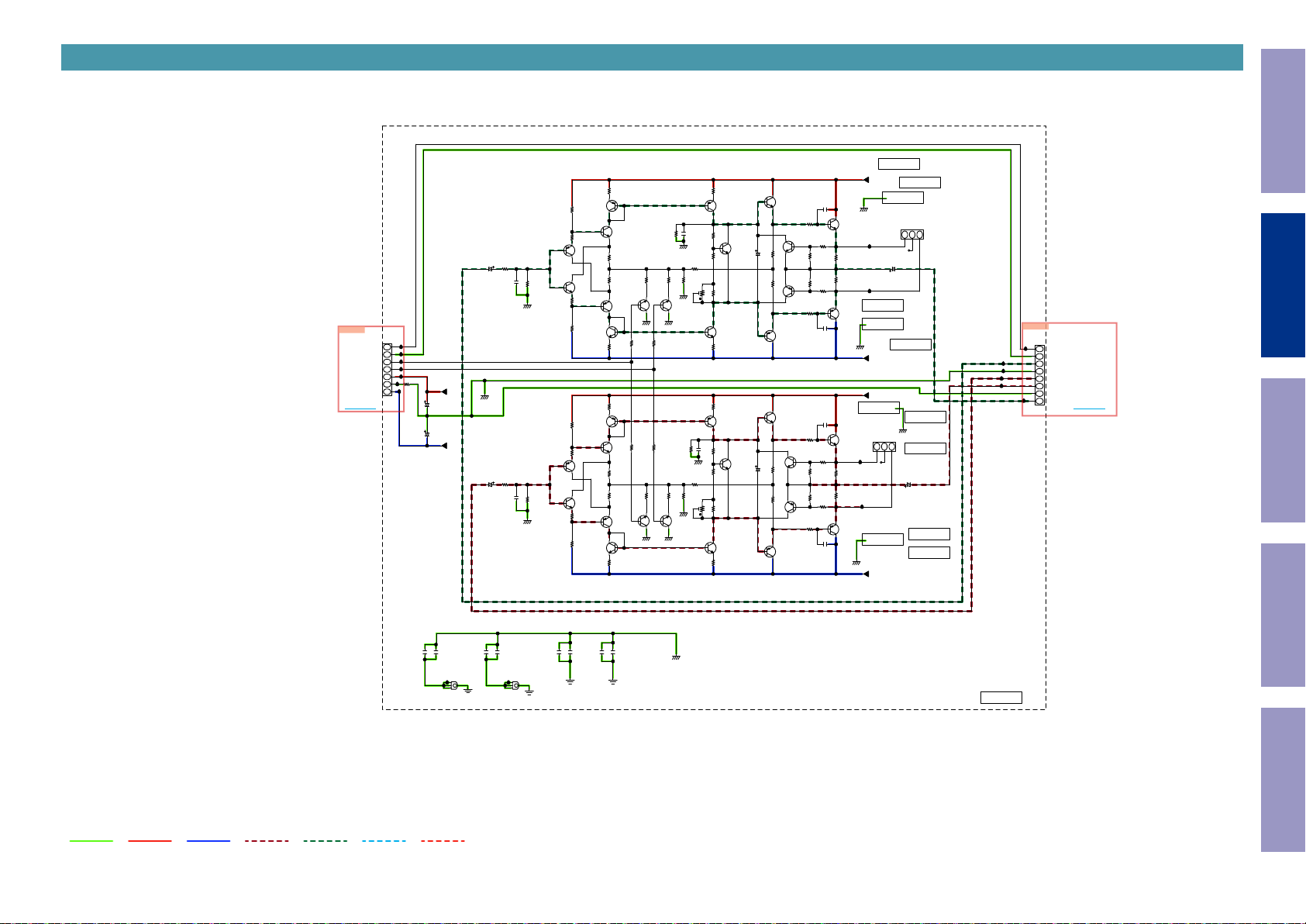
SCH07_DIGITAL(3/7)
+3.3V_D5.
2A
B6
TO A2
FROM PLD
TO 6B
from μCOM
PLL2_TXD
PLL2_CLK
BE_CLK#
PLL1_TXD
PLL1_CLK
22.5792MHZ
.24.576MHZ
DAC_FS_CONT.
BIDIRECT
BIDIRECT
BIDIRECT
BIDIRECT
BIDIRECT
BIDIRECT
BIDIRECT
BIDIRECT
OPENR579
GND-TERM(SD01388-28)
B504
GND-TERM(SD01388-28)
B505
OPENR580
1
2
3
4
5
33
R582
R583
33
1
2
3
R581
4
33
5
R584
33
GND-TERM(SD01388-28)
B506
U319
CS2000-CP
VD
GND
CLKO
AUXO
XTI
CLKIN
XTO
R587
10K
U320
CS2000-CP
VD
GND
CLKO
AUXO
XTI
CLKIN
XTO
All Ref.No. has been described in the parts list are four digits.
But there are less than four digits of printed Ref.No. on the PCB, and they have become four digits after the header by adding "0" in the parts list.
Caution in
servicing
Electrical Mechanical Repair Information Updating
+3.3V_D5.
C579 0.01
1000P
C580
U321
16
1
VCC
27M_PLL1
R594
33
GND
TP_PLL
FCX-05(27.000MHz)
74VHC157FT(BJ)
X302
SE
15
2
ST
1A
14
3
4A
1B
13
4
4B
1Y
5
12
4Y
2A
11
6
3A
2B
10
7
3B
2Y
9
8
3Y
GND
+3.3V_D5.
L315
11A121
L314
11A121
R597
22K
R595
10K
C581
2200P
PLL_GND
R596
OPEN
100
R598
1 3
5P
5P
C549
C548
GND
0
R593
+3.3V_D5.
L312
11A121
C577
R585
10K
10K
R589
0.1
10
M0
9
M1
8
M2
7
6
10K
R586
R592
33
27M_PLL2
GND
+3.3V_D5.
L313
11A121
C578
0.1
R590
10K
10
M0
9
M1
8
M2
7
6
10K
R588
R591
33
GND
33
C584
C582
C583
R601
C585
10/6.3
R599
33
10/6.3
R600
0
10/6.3
10/6.3
C590 0.01
1000P
C591
U324
14
1
VCC
CD1
13
2
D1
3
CP1
4
SD1
5
Q1
6
Q1
7
GND
TC74VHC74FT
R604
CD2
0
12
D2
R605
11
CP2
0
10
SD2
9
Q2
8
Q2
GND
C589
U323
0.1
SM5158AM-G
16
OR
1
XIN
15
OV
2
XOUT
14
TEST
3
FV
13
FR
4
VDD
DOA
5
12
DOP
11
LE
6
VSS
10
DATA
7
LD
CLK
9
8
FIN
OPEN
R602
C588
0.1
U322
BU2365FV
1
CLK54M
24
VDD54M
2
OE
23
VSS54M
3
768FS
22
FSEL
4
VDD
21
TEST
5
VSS
20
AVDD
0.1
C587
6
384FS
19
AVSS
7
512FS
18
XTALI
8
VDDB
17
XTALO
9
BUFI
16
VDDV
VSSB
15
10
VCTRL
BUFO1
14
11
VSSV
BUFO2
13
12
VCXO
C586
0.1
OPEN
R603
R610
R611
R607 OPEN
R608
R609 OPEN
C593
C592
0.1
10/6.3
3A
BIDIRECT
VCXO_CS
BIDIRECT
VCXO_TXD
BIDIRECT
VCXO_CLK
BIDIRECT
OPEN
R606
33
0
0
PLL_LD
TO A3
+3.3V_D5.
to BE
R612
47
GND
C594 0.01
1000P
C595
R613
0
U325
16
1
VCC
SE
15
2
ST
1A
14
3
4A
1B
13
4
4B
1Y
5
12
4Y
2A
GND
R614
11
6
3A
2B
10
7
3B
2Y
33
9
8
3Y
GND
74VHC157FT(BJ)
GND
8501_27MHZ
GND LINE
POWER+ LINE
C557
1000P
C558
1000P
C559
1000P
C560
100P
C561
100P
GND
FG_2
POWER- LINE
C567
C562
1000P
1000P
C568
C563
1000P
1000P
C564
C569
1000P
1000P
C570
C565
100P
100P
C566
C571
100P
GND
100P
GND
FG_4
FG_3
ANALOG AUDIO R ANALOG AUDIO L
DIGITAL AUDIO
8U-310213
Digital UNIT(3/7)
STBY POWER
15
SCH08_DIGITAL(4/7)
D706
KDS122
2
1
3
R713
OPEN
C.GND7
USB_DN
USB_VBUS
X1D34
GND LINE
E19
3V3
0
R701
0.01Z
C702
GND_B
USB_DN
USB_DP
R715
OPEN
GND_B
GND_B
0.1Z
C704
22/6.3
C705
GND_B
POWER+ LINE
INPUT
INPUT
R702
0
3V3
C707
0.1Z
R703
R704
R705
R706
R707
R708
R709
R710
3V3_IO
VDDCORE
L702
4.7u
1V8
L703
4.7u
22/6.3
C708
GND_B
MODE[0]
G1
L18
MODE[1]
USB_DP
K18
H1
MODE[2]
J18
MODE[3]
H18
MODE[4]
USB_ID
G18
H2
USB_VBUS
G2
OSC_EXT_N
R712
OPEN
GND_B
R711
0
0
0
0
0
0
0
0
0
L6
XC_TDO
K19
AVDD
XC_TDI
N1
N19
XC_TMS
M19
XC_TCK
L19
ADC0
R1
DEBUG_N
ADC1
M18
R2
ADC2
P1
ADC3
RST_N
P2
J2
ADC4
M1
XO
ADC5
V1
M2
ADC6
XI/CLK
L1
U1
ADC7
L2
NC
NC
N2
U2
NC
NC
N18
M7
NC
NC
P18
N7
NC
NC
R18
N6
NC
NC
T1
M6
NC
T2
NC
T18
NC
U18
NC
V2
NC
V12
NC
V18
NC
W2
NC
W12
PSUP
VDDIO
K1
V7
PSUP
VDDIO
W1
K2
PSUP
W7
VDDIO_OUT
F18
VDDCORE
V3
VDDCORE
W4
VDDCORE
W3
SW1
V6
SW1
W6
VDD1V8
V8
VDD1V8
W8
VDD1V8
W9
SW2
V11
SW2
F6
W11
GND_B
F7
GND_B
F8
GND_B
F9
GND_B
F10
GND_B
F11
GND_B
F12
L7
GND_B
GND_B
F13
L8
GND_B
GND_B
L9
F14
GND_B
GND_B
L10
G6
GND_B
GND_B
L11
G7
GND_B
GND_B
G8
L12
GND_B
GND_B
L13
G9
GND_B
GND_B
G10
L14
GND_B
GND_B
G11
M8
GND_B
GND_B
G12
M9
GND_B
GND_B
G13
M10
GND_B
GND_B
M11
G14
GND_B
GND_B
M12
H6
GND_B
GND_B
H7
M13
GND_B
GND_B
M14
H8
GND_B
GND_B
N8
H9
GND_B
GND_B
N9
H10
GND_B
GND_B
N10
H11
GND_B
GND_B
N11
H12
GND_B
GND_B
H13
N12
GND_B
GND_B
N13
H14
GND_B
GND_B
J6
N14
GND_B
GND_B
P6
J7
GND_B
GND_B
J8
P7
GND_B
GND_B
P8
J9
GND_B
GND_B
J10
P9
GND_B
GND_B
P10
J11
GND_B
GND_B
P11
J12
GND_B
GND_B
J13
P12
GND_B
GND_B
J14
P13
GND_B
GND_B
P14
K6
GND_B
GND_B
K7
GND_B
K8
GND_B
V4
K9
GND_B
(PGND)
GND_B
K10
V5
GND_B
(PGND)
GND_B
K11
V9
GND_B
GND_B
(PGND)
V10
K12
GND_B
(PGND)
GND_B
K13
W5
GND_B
(PGND)
GND_B
K14
W10
(PGND)
GND_B
GND_B
GND_B GND_B
POWER- LINE
差動Z = 90Ω
GND
4
N701
D+
3
D-
2
VCC
1
UBR24-4K5G00
0
0
0
0
D702
D703
D701
C711
C710
C713
C714
CG0603MLC-12LE
CG0603MLC-12LE
CG0603MLC-12LE
R714
R722
0
R718
0
INPUT
XC_MSEL
0
R719
R720
0
R721
0
GND_B
INPUT
XC_TDO
INPUT
XC_TDI
INPUT
XC_TMS
INPUT
XC_TCK
R716
0
INPUT
BRD_RST_N
R717
0
INPUT
XCORE_CLK
3V3
0
R723
0.1Z
4.7u
0.01Z
C712
C715
C716
GND_B
GND_B
3V3
0.1Z
0.1Z
0.01Z
C717
220/6.3
C721
C719
C723
GND_B
3V3
0.1Z
0.1Z
0.01Z
C718
220/6.3
C720
C722
C724
GND_B
ANALOG AUDIO R ANALOG AUDIO L
All Ref.No. has been described in the parts list are four digits.
But there are less than four digits of printed Ref.No. on the PCB, and they have become four digits after the header by adding "0" in the parts list.
Caution in
servicing
OUTPUT
USBB_VBUS
INPUT
USB_DP
INPUT
USB_DN
3V3
GND_B
R772
0
270
A
C
4
1
2
K3E
TLP185
GND_B
U713
1A2 3 4 5 6 7 8 9
X1D05A2X1D06A3X1D07A4X1D08A5X1D09A6X1D10A7X1D11A8X1D12A9X1D13
A1
X1D05
X1D04
B1
B
X1D04
X1D03
C1
C
X1D03
X1D02D2X1D51
D1
D
X1D02
X1D01E2X1D50
E1
E
X1D01
X1D00F2X1D49
F1
F
I2C_SLV_SDA
USB_DNG2USB_VBUS
G1
G
USB_DN
USB_DPH2USB_ID
H1
H
USB_DP
X0D43/WAKEJ2RST_N
J1
J
X0D43/WAKE
VDDIOK2VDDIO
K1
K
VDDIO
ADC6L2ADC7
L1
L
ADC6
ADC4M2ADC5
M1
M
ADC4
AVDDN2NC
N1
N
AVDD
ADC2P2ADC3
P1
P
ADC2
ADC0R2ADC1
R1
R
ADC0
T1NCT2
T
XI/CLKU2NC
U1
U
XI/CLK
V1XOV2NCV3
V
XO
PSUPW2NCW3VDDCOREW4VDDCOREW5PGNDW6SW1W7PSUPW8VDD1V8W9VDD1V8
W1
W
PSUP
U701
X1D08
X1D07
X1D06
X1D53B3X1D54B4X1D55B5X1D56B6X1D57B7X1D58B8X1D61B9X1D62
B2
X1D54
X1D55
X1D53
C2
X1D52
X1D52
X1D51
X1D50
X1D49
USB_VBUS
USB_ID
RST_N
VDDIO
ADC7
ADC5
ADC3
ADC1
NC
VDDCOREV4PGNDV5PGNDV6SW1V7PSUPV8VDD1V8V9PGND
VDDCORE
GND_B
(PGND)
VDDCORE
VDDCORE
XS1-U8A-128-FB217
B19
B18
X1D25
X1D24
I2C_SLV_SCL
X1D09
X1D56
X1D57
GNDF7GNDF8GNDF9GND
F6
GND_B
GND
G6
GND_B
GND
H7
H6
GND_B
GNDJ7GND
J6
GND_B
GNDK7GNDK8GND
K6
GND_B
OSC_EXT_NL7GNDL8GNDL9GND
L6
OSC_EXT_N
M6NCM7NCM8
N6NCN7NCN8
GNDP7GNDP8GNDP9GND
P6
GND_B
SW1
GND_B
(PGND)
SW1
GND_B
(PGND)
F19
X1D36
SDIN1
MCLK_XCORE
X1D58
GND_B
GNDG8GNDG9GND
G7
GND_B
GND
H8
GND_B
J8
GND_B
GND_B
GND_B
GND_B
PSUP
PSUP
H19
J19
G19
X1D38
X1D39
X1D37
10 11 12 13 14 15 16 17 18 19
X1D14
A10
LRCK
X1D14
X1D63
B10
X1D61
X1D62
X1D63
GND
F10
GND_B
GND_B
GND_B
GND
G10
GND_B
GND_B
GND_B
GNDH9GND
GND
H10
GND_B
GND_B
GND
GND
GND
J9
J10
GND_B
GND_B
GND_B
GND
GND
K9
K10
GND_B
GND_B
GND_B
GND
L10
GND_B
GND_B
GND_B
GNDM9GND
GND
M10
GND_B
GND_B
GND_B
GNDN9GND
GND
N10
GND_B
GND_B
GND_B
GND
P10
GND_B
GND_B
GND_B
PGND
V10
1V8
GND_B
GND_B
(PGND)
(PGND)
PGND
W10
1V8
1V8
GND_B
(PGND)
W19
X0D12
X1D15
A11
X1D15
X1D64
B11
X1D64
F11
GND_B
G11
GND_B
H11
GND_B
J11
GND_B
K11
GND_B
L11
GND_B
M11
GND_B
N11
GND_B
P11
GND_B
V11
SW2
W11
SW2
P19
V13
W13
X0D24
X0D22
X0D35
X1D16
A12
A13
X1D16
X1D65
B12
B13
X1D65
GND
GND
F12
F13
GND_B
GND
GND
G12
G13
GND_B GND_B
GND
GND
H12
H13
GND_B
GND
GND
J12
J13
GND_B
GND
GND
K12
K13
GND_B
GND
GND
L12
L13
GND_B
GND
GND
M12
M13
GND_B
GND
GND
N12
N13
GND_B
GND
GND
P13
P12
GND_B
SW2
V12NCV13
SW2
W12NCW13
X1D17
X1D66
GND_B
GND_B
GND_BGND_B
GND_B
GND_B
GND_B
GND_B
GND_B
GND_B
X0D24
X0D22
33_VCC_USB-B
0.1Z
C725
3V3 1V8
U702
NC7SZU04
5
2 4
0.01Z
3
1
C726
GND_B
2.2MR727
X701
FCX04(24MHZ)
15P
C727
U703
NC7SZ125
1
5
OUTPUT
2 4
R730
33
33_VCC_USB-B
3
GND_B
R728
680
1V8
0
R729
0.01Z
15P
C728
C730
C729
GND_BGND_B
XCORE_CLK
R731
C0
USBB_DETECT
0.1Z
TO 0C
OPEN
A
C
OUTPUT
4
1
2
K3E
TLP185
U704
GND
Q704
KRA102S
0.1
GND_B
C731
USBB_VBUS
OUTPUT
R732
270
GND_B
8U-310213
X1D17
A14
X1D66
B14
GND
F14
GND
G14
GND
H14
GND
J14
GND
K14
GND
L14
GND
M14
GND
N14
GND
P14
X0D24
V14
X0D22
W14
Q705
KRC102S
D1
E1
A12
C18
X1D16
X1D02
X1D26
X1D01
3V3
X1D18
X1D19
X1D20
X1D21
X1D22
X1D70
X0D15
X0D14
A18
SCLK
X1D24
B18
X1D24
X1D26
C18
X1D26
X1D33
D18
DSD_MODE
X1D35
E18
X1D35
VDDIO_OUT
F18
VDDIO_OUT
MODE[4]
G18
MODE[4]
MODE[3]
H18
MODE[3]
MODE[2]
J18
MODE[2]
MODE[1]
K18
MODE[1]
MODE[0]
L18
MODE[0]
DEBUG_N
M18
DEBUG_N
N18NCN19
P18NCP19
R18NCR19
T18NCT19
U18NCU19
V18NCV19
X0D13
W18
X0D13
SPI_CS_N
SPI_MISO
T19
R19
A19
B19
C19
INT_REQ_N
D19
MCLK_FSEL
E19
USB_VBUS
F19
G19
H19
J19
K19
L19
M19
W19
SPI_MISO
SPI_CS_N
XC_TDO
XC_TCK
XC_TMS
XC_TDI
SPI_CLK
SPI_MOSI
X1D23
R734
X1D25
X1D27
X1D32
X1D34
X1D36
X1D37
X1D38
X1D39
4.7K
A6
I2C_SLV_SCL
F1
I2C_SLV_SDA
R735
SCLK
A18
R736
LRCK
A9
R737
SDIN1
A7
R738
SDIN2
A19
3V3
4.7K
R739
INT_REQ_N
C19
MCLK_FSEL
D19
X1D35
E18
DSD_MODE
D18
MUTE_A
A14
TDO
X0D13
W18
TCK
MCLK_XCORE
A8
TMS
SDIN2
X1D25
X1D36
X1D37
X1D38
X1D39
TDI
X0D35
X0D35
X0D00
BRD_RST_N
INPUT
X0D01
X0D10
X0D11
X0D12
X0D12
10K
10K
U705
R733
R787
MX25L4006EM1I-12G
CS#
VCC
1
8
SO
HOLD#
2
7
WP#
SCLK
3
6
GND
SI
4
5
A15
A16
A17
X1D19
MUTE_A
X1D20
X1D67
B15
X1D67
X1D21
X1D68
X1D69
B16
B17
X1D69
X1D68
X1D70
GND
GND_B
GND
GND
GND_B
GND
GND_B
GND
GND_B
GND
GND_B
GND
GND_B
GND
GND_B
GND
GND_B
X0D21
X0D19
X0D17
V17
V15
V16
XL_DN1.
XL_UP0.
XL_DN0.
+5V_SPDIF
1SS301
S701
4 2
5 7
X0D15
X0D18
X0D16
W16
W17
XL_UP1.
X0D14
18
1
S701
3
2
G6K-2F-Y-TR
GND
3
6
GND_B
X0D21
X0D20
W15
X0D20
Q706
KRA102S
D704
G6K-2F-Y-TR
GND
4.7K
R740
4.7K
R788
GND_B
GND_B
3V3
GND_B
100/6.3
C770
R741
4.7K
0
R742
R743
0
100
33
33
33
R745
33
R746
33
R759
33
R747
33
R748
33
R749
33
R744
0.1Z
C734
KRC102S
GND_B
3V33V3
0.1Z
0.01Z
C732
C733
D705
KDS160
非標準部品
U770
NJM2845DL1-33
IN
OUT
3V3
GND_B
GND_B
GND_B
GND_B
0.1Z
GND_B
Q708
KRA102S
0.1
0.1
100/16
C772
C774
C773
C740
0.1Z
GND_B
C738
0.1Z
C736
0.1Z
C741
0.1Z
C739
0.1Z
R781
100
R750
100
C735
ADuM1285CRZ
GND_B
R752
33
0.1
C771
3V33V3
10K
Q707
DEBUG ONLY
INPUT
XC_MSEL
INPUT
XC_TDI
INPUT
XC_TMS
INPUT
XC_TCK
INPUT
XC_TDO
INPUT
BRD_RST_N
SPI_CLK
U19
SPI_MOSI
V19
0.01
1000P
C776
C775
5
GND1
GND2
6
SCL1
SCL2
SDA1
SDA2
7
VDD1
VDD2
8
ADuM1250ARZ
U711
U706
ADuM1285CRZ
1
VDD1
VDD2
VIA
2
VOA
VOB
3
VIB
GND15GND2
4
U707
ADuM1285CRZ
1
VDD2
VDD1
2
VIA
VOA
3
VOB
VIB
4
GND2
GND1
U708
ADuM1280ARZ
1
VDD1
VDD2
VIA
2
VOA
VIB
VOB
3
GND2
GND1
4
U709
ADuM1280ARZ
1
VDD1
VDD2
2
VOA
VIA
3
VOB
VIB
GND2
4
GND1
5
GND2
GND1
6
VOB
VIB
7
VIA
VOA
8
VDD2
VDD1
U712
4
3
2
1
8
7
6
8
7
6
5
8
7
6
5
8
7
6
5
4
3
2
1
N702
OPEN
1
3
5
7
9
11
13
15
17
19
N304
N304
3P-PH
1
+4V_USBB
2
GND_USBB
3
GND_USBB
TO N314
GND
GND
C743
0.1Z
C744
0.1Z
C745
0.1Z
C746
0.1Z
C747
0.1Z
C742
220/6.3
2
4
6
8
10
12
14
16
18
20
GND_B
33_VCC_USB-B
10K
R782
C749
0.1Z
GND
R755
R756
10K
R783
33_VCC_USB-B
R757
R758
GND
R762
R763
GNDGND
R764
R765
R766
R767
R768
R769
GND
3B
0
R760
BIDIRECT
I2C_SCL_1
0
R761
100
33
33
33
TO B3
BIDIRECT
I2C_SDA_1
B7
TO 7B
OUTPUT
USBB_PBCK.
OUTPUT
USBB_PLRCK/DBCK.
OUTPUT
33
PDATA/DSD_DATA_L.
OUTPUT
33
USBB_DSD_DATA_R.
B8
TO 8B
OUTPUT
33
USBB_INT_REQ_N.
OUTPUT
33
USBB_MCLK_FSEL.
OUTPUT
33
DSD_MODE_DSD/PCM.
OUTPUT
33
USBB_MUTE_1
B9
TO 9B
INPUT
0
USBB_MCLK.
INPUT
33
USBB_RST.
XL_UP1.
W16
XL_UP0.
V16
XL_DN0.
W15
XL_DN1.
V15
Electrical Mechanical Repair Information Updating
Digital UNIT(4/7)
DIGITAL AUDIO
STBY POWER
16

SCH09_DIGITAL(5/7)
6B
TO B6
0B
TO B0
1B
TO B1
4B
TO B4
C1
TO 1C
9B
TO B9
7B
TO B7
C2
TO 2C
N3901
TO N4101
5A
TO A5
7A
TO A7
GND LINE
7P-FFC
(for PLD update)
N3901
to MCU
3.3V
to PLL and DIR
to PLD and
VCXO UNIT
to DIR
4137_DATAO
to u-com/MECHA UNIT
USBB_MCLK.
USBB_PBCK.
USBB_PLRCK/DBCK.
PDATA/DSD_DATA_L.
USBB_DSD_DATA_R.
USBB_MCLK_FSEL.
to XMOS
USBB_DSD_PCM.
1
TCK
2
GND
3
TDO
4
5
TMS
6
TDI
7
GND
ERROR
MZ_SIG_SEL
MZ_EMPHA
PLD_VER_CONT
MTK_MODE
SPDIF_MODE
USB-B_MODE
PCM_DSD_MODE
MCK_FS_CONT
FS384_CONT
PLL1_CLK
PLL1_TXD
DSP_WDT_RSTO
DAC_FS_CONT.
22.5792MHZ
24.576MHZ
.24.576MHZ
PLD_OUT_LRCK
PLD_OUT_DATA
PLD_OUT_BCK
PLD_OUT_MCK
DIR1_MCK
DIR1_DATA
DIR1_LRCK
DIR1_BCK
4137_LRCKO
D_OUT_MECHA
RES_MCK
I2S_MCLK
PBCK/DBCK
PLRCK
PDATA/DSDL
DSDR
33_VCCIO
VOLT_PROT_A
HPGAIN_MID
HPGAIN_HI
DSD/PCM
AMUTE
PLD_RES4
PLD_RES2
MZ_TEST3
MZ_TEST4
MZ_TEST5
PLD_DSP2_TEST0
A_MUTE
POWER+ LINE
4137_MCKI
4137_BCKO
CH_SYNC_I
GND
OUTPUT
OUTPUT
OUTPUT
OUTPUT
OUTPUT
OUTPUT
OUTPUT
OUTPUT
OUTPUT
OUTPUT
OUTPUT
OUTPUT
OUTPUT
TCK
TDO
TMS
TDI
INPUT
INPUT
INPUT
OUTPUT
OUTPUT
OUTPUT
INPUT
INPUT
INPUT
OUTPUT
INPUT
OUTPUT
OUTPUT
OUTPUT
OUTPUT
OUTPUT
OUTPUT
INPUT
OUTPUT
OUTPUT
INPUT
OUTPUT
OUTPUT
OUTPUT
DAC_FS_CONT.
INPUT
INPUT
INPUT
INPUT
INPUT
INPUT
INPUT
INPUT
INPUT
INPUT
INPUT
INPUT
INPUT
INPUT
INPUT
INPUT
INPUT
VOLT_PROT_A
22.5792MHZ
24.576MHZ
.24.576MHZ
PLD_OUT_MCK
DIR1_MCK
DIR1_DATA
DIR1_LRCK
DIR1_BCK
D_OUT_MECHA
I2S_MCLK
PBCK/DBCK
PDATA/DSDL
USBB_MCLK.
USBB_PBCK.
USBB_PLRCK/DBCK.
PDATA/DSD_DATA_L.
USBB_DSD_DATA_R.
USBB_MCLK_FSEL.
USBB_DSD_PCM.
HPGAIN_MID
HPGAIN_HI
DSD/PCM
INPUT
AMUTE
INPUT
ERROR
PLD_RES4
PLD_RES2
MZ_TEST3
MZ_TEST4
MZ_TEST5
MZ_SIG_SEL
MZ_EMPHA
PLD_VER_CONT
MTK_MODE
SPDIF_MODE
USB-B_MODE
PCM_DSD_MODE
MCK_FS_CONT
FS384_CONT
PLD_DSP2_TEST0
CH_SYNC_I
PLL1_CLK
PLL1_TXD
A_MUTE
DSP_WDT_RSTO
POWER- LINE
RES_MCK
GND
33_VCCIO
47/6.3
C801
NJM2845DL1-18
4137_MCKI
4137_BCKO
4137_LRCKO
4137_DATAO
PLRCK
DSDR
WDT_P1
PLD_DATA_OUT
PLD_LRCK_OUT
PLD_BCK_OUT
PLD_OUT_MCK
DSD_LRCK
DSPDSD_R
DSPDSD_L
DSD_BCK
DSP2_TEST_0
CH_SYNC_2
WDT_P2
4137_MCKI
4137_BCKO
4137_LRCKO
4137_DATAO
PLD_FS1
PHASE_INV
PLD_FS0
DAC_FS_CONT.
INFO_ERR
ANALOG AUDIO R ANALOG AUDIO L
D801
KDS160
IN
OUT
0.1
C802
U802
-
GND
R842
R822
R820
R824
R818
R836
R828
R826
R830
R853
R856
R859
R870
R868
R847
R844
signal name
PLD_RES4
PLD_RES2
MZ_SIG_SEL
PLD_DSP2_TEST0
SEL_DIR/Other.
SPDIF_MODE
0.1
47/6.3
C803
C804
C805
47
47
47
47
47
0
0
C807
C808
0
0
47
47
47
47
47
47
47
actual function
PLD_FS1
PHASE_INV
PLD_FS0
INFO_ERROR
HP_OFF_OUT
HP_OFF_IN
DIGITAL AUDIO
0.1
1000P
0.1
C809
C810
1.8V_core
C806
1000P
100/16
0.1
-
GND
L802
NFM18PS105R0J3
HP_OFF_OUT
STBY POWER
L804
100/16
C812
0.1
C811
1
GND
2
3
4
5
.PLD_BCK_OUT
6
.PLD_MCK_OUT
.DSD_LRCK
7
8
.DSPDSD_R
9
33_VCCIO
GND
10
GND
11
.DSPDSD_L
12
1.8V_core
13
.DSD_BCK
14
.DSP2_TEST_0
15
.CH_SYNC_2
16
.WDT_P2
17
.DSP2_FLAG3
18
.DSP2_FLAG0
19
.DSP1_FLAG3
20
.DSP1_FLAG0
21
TMS
22
TDI
23
TCK
24
TDO
25
CH_SYNC_1
DSP1_TEST_0
USBB_MCLK_FSEL.
NFM18PS105R0J3
0
47
47
R815
R840
R838
98
99
100
.CH_SYNC_1
.DSP1_TEST_0
.USBB_MCLK_FSEL.
.reserved_2
.DAC_FS_CONT.
.SEL_DIR/Other.
27
28
26
0
0
33
R895
R904
R906
SEL_DIR/Other.
PLD_FILTER..
USBB_DSD_DATA_R.
0
R814
C813
0
R894
49M_OUT..
97
.USBB_DSD_DATA_R.
.49MHz..
29
45M_OUT..
PDATA/DSD_DATA_L.
0
R813
1000P
0
R891
USBB_MCLK.
USBB_PBCK.
USBB_PLRCK/DBCK.
0
100
0
R812
R811
R810
0.1
C814
94
95
96
33_VCCIO
.USBB_PLRCK/DBCK.
.PDATA/DSD_DATA_L.
.WDT_P1
.PLD_DATA_OUT
.PLD_LRCK_OUT
GND
33_VCCIO
.45MHz..
32
31
30
C815
OPEN
R890
All Ref.No. has been described in the parts list are four digits.
But there are less than four digits of printed Ref.No. on the PCB, and they have become four digits after the header by adding "0" in the parts list.
.24.576MHZ
22.5792MHZ
47
47
R907
R850
1000P
C816
91
92
93
GND
.USBB_MCLK.
.USBB_PBCK.
.DIR_MCK
.reserver_1
.reserved_0
35
34
33
0.1
33
OPEN
R889
R888
DIRMCK..
ERROR
CH_SYNC_I
24.576MHZ
0
0
47
47
R881
R878
R823
R872
87
88
89
90
.ERROR
.24MHZ_OUT
.CH_SYNC_I
.22MHZ_OUT
BANK_2: 52-100PIN
U801
5M240ZT100C5N
BANK_1: 2-51PIN
.OUT_DSDBCK
.OUT_DSDLN
.OUT_DSDR
.OUT_DSDRN
39
38
37
36
33
33
33
33
100
R886
R885
R887
R892
R893
DSDBCK..
DSDRN..
DSDR..
DSDLN..
DSDL..
MZ_TEST4
MZ_TEST3
47
47
47
47
R841
R839
R857
R854
82
84
86
83
.FS1.85.FS0.
.MZ_TEST4
.MZ_TEST3
.PLD_DSP1_TEST0
CLKIN.
.PLD_DSP1_TEST1
.PBCK/DBCK
.PLRCK
.DSDR42.PD ATA/DSDL
.OUT_DSDL
41
40
44
43
C817
1000P
0
0
0
0
R807
R808
R809
R806
DSDR
PDATA/DSDL
PLRCK
PBCK/DBCK
MZ_TEST5
MZ_SIG_SEL
47
47
R843
R845
0.1
1000P
C818
C820
80
81
78
79
GND
.PLD_FS0
33_VCCIO
.MZ_TEST5
CLKO
.USB-B_MODE
.SPDIF_MODE
.FS384_CONT
.MCK_FS_CONT
.PLD_DSP1_TEST2
.PCM_DSD_MODE
.USBB_DSD_PCM.
.DIR1_DATA
.D_OUT_MECHA
.I2S_MCLK
GND
33_VCCIO
46
48
47
45
C819
0.1
0
47
R816
R805
I2S_MCLK
D_OUT_MECHA
PLD_VER_CONT
MZ_EMPHA
47
47
R851
R848
77
76
.MZ_EMPHA
.PLD_VER_CONT
.PLD_RES1
.MTK_MODE
.PHASE_INV
1.8V_core
.A_MUTE
.PLD_FS1
33_VCCIO
.INFO_ERR
.DIR1_MCK
.DIR1_LRCK
.DIR1_BCK
.DSD/PCM
.AMUTE
.RES_MCK
49
50
0
0
R819
R905
RES_MCK
AMUTE
C3
TO 3C
to DSP1 to DSP2
DSD_LRCK.
DSD_BCK.
PLD_BCK_OUT.
PLD_LRCK_OUT.
PLD_DATA_OUT.
24M_DSP1
OUTPUT
OUTPUT
CH_SYNC_1
DSP1_TEST_0
DSPDSD_L.
DSPDSD_R.
OUTPUT
OUTPUT
OUTPUT
OUTPUT
INPUT
INPUT
INPUT
INPUT
47
47
47
OPEN
47
R861
PLD_LRCK_OUT
OPEN
GND
1
VD
GND
2
CLKO
3
4
5
R908
100
R858
PLD_BCK_OUT
DSPDSD_L
PLD_DATA_OUT
U803
M0
10
M1
9
M2
8
XTI
7
AUXO
XTO
6
CLKIN
R898
OPEN
U901
TC7WHU04FU
1A
1
2Y
2
3A
3
GND43Y
R867
R860
R863
R864
R865
R866
DSPDSD_R
OPEN
OPEN
R900
R899
R911
VCC
8
1Y
7
2A
6
5
47
47
47
47
CH_SYNC_1
DSP1_TEST_0
OPEN
R901
HP_OFF_IN
OPEN
R84647R84947R85247R855
R832
47
R833
47
R834
47
33_VCCIO
L805
OPEN
75
74
73
72
71
70
69
68
67
66
GND
65
64
63
62
C822
61
GND
60
59
58
C824
57
56
55
54
53
52
51
C821
1000P
C823
1000P
R896
R877
R837
R862
R871
R869
0.1
R827
0.1
R873
R825
R821
R801
R802
R803
R804
R817
C825
OPEN
R897
OPEN
CLKO
GND
CLKIN
22
47
47
47
47
47
OPENR875
R874
47
47
R876
47
R3013
R831
47
47
47
0
0
0
DIR1_DATA
0
0
DIR1_LRCK
0
0
DIR1_MCK
DIR1_BCK
USBB_DSD_PCM.
45M_OUT..
49M_OUT..
R902
WDT_P1
OPEN
R909
1M
33
R910
INPUT
WDT_P1
C902
0.01
1000P
C901
U804
OPEN
2 3
GND
PLD_DSP2_TEST0
33_VCCIO
R912
0.01
100
0.1
C904
C903
C4
24M_DSP2
OUTPUT
4
OPEN
R903
1
PLL1_TXD
PLL1_CLK
MTK_MODE
USB-B_MODE
SPDIF_MODE
FS384_CONT
MCK_FS_CONT
DSP_WDT_RSTO
PLD_RES2
A_MUTE
PLD_RES4
PCM_DSD_MODE
DSD/PCM
U902
TC7WHU04FU
1A
1
2Y
2
3A
3
GND43Y
TO 4C
PLD_LRCK_OUT..
PLD_DATA_OUT..
PLD_BCK_OUT..
DSD_LRCK..
DSD_BCK..
WDT_P2
CH_SYNC_2
DSPDSD_L..
DSPDSD_R..
OUTPUT
8
7
6
5
OUTPUT
INPUT
INPUT
OPEN
R879
33_VCCIO
DSDL..
DSDLN..
DSDR..
DSDRN..
DSDBCK..
DIRMCK..
45M_OUT..
49M_OUT..
PLD_FILTER..
A_MUTE
SEL_DIR/Other.
VOLT_PROT_A
HPGAIN_HI
HPGAIN_MID
R913
1M
R914
100
R882
47
R880
DSD_BCK
33
OUTPUT
OUTPUT
DSD_LRCK
R916
R917
1000P
C905
DSP2_TEST_0
INPUT
INPUT
INPUT
47
R884
WDT_P2
CH_SYNC_2
DSP2_TEST_0
L807
BLM21PG221
OPEN
OPEN
R883
C906
0.01
OPENR915
33_VCCIO
0.1
0.01
C908
C907
N4001
N4001
40P-FFC
1
33_VCCIO
2
33_VCCIO
3
GND
4
DSDL
5
GND
6
DSDLN
7
GND
8
DSDR
9
GND
DSDRN
10
GND
11
12
13
14
15
16
17
18
19
20
21
22
23
24
25
100
26
27
28
29
30
31
32
33
34
35
36
GND
37
38
39
40
DSDBCK
GND
DIRMCK
GND
GND
GND
GND
GND
45M_OUT
GND
49M_OUT
GND
GND
PLD_FILTER
MUTE
SEL_44/48
SEL_DIR/OTHER
GND
VOLT_PROT_A
HPGAIN_HI
HPGAIN_MID
GND
GND
GND
GND
GND
GND
GND
GND
AUDIO UNIT
(G-1)
to DAC
TO N7005
OUTPUT
OPEN
C826
VCC
1Y
2A
Caution in
servicing
Electrical Mechanical Repair Information Updating
17
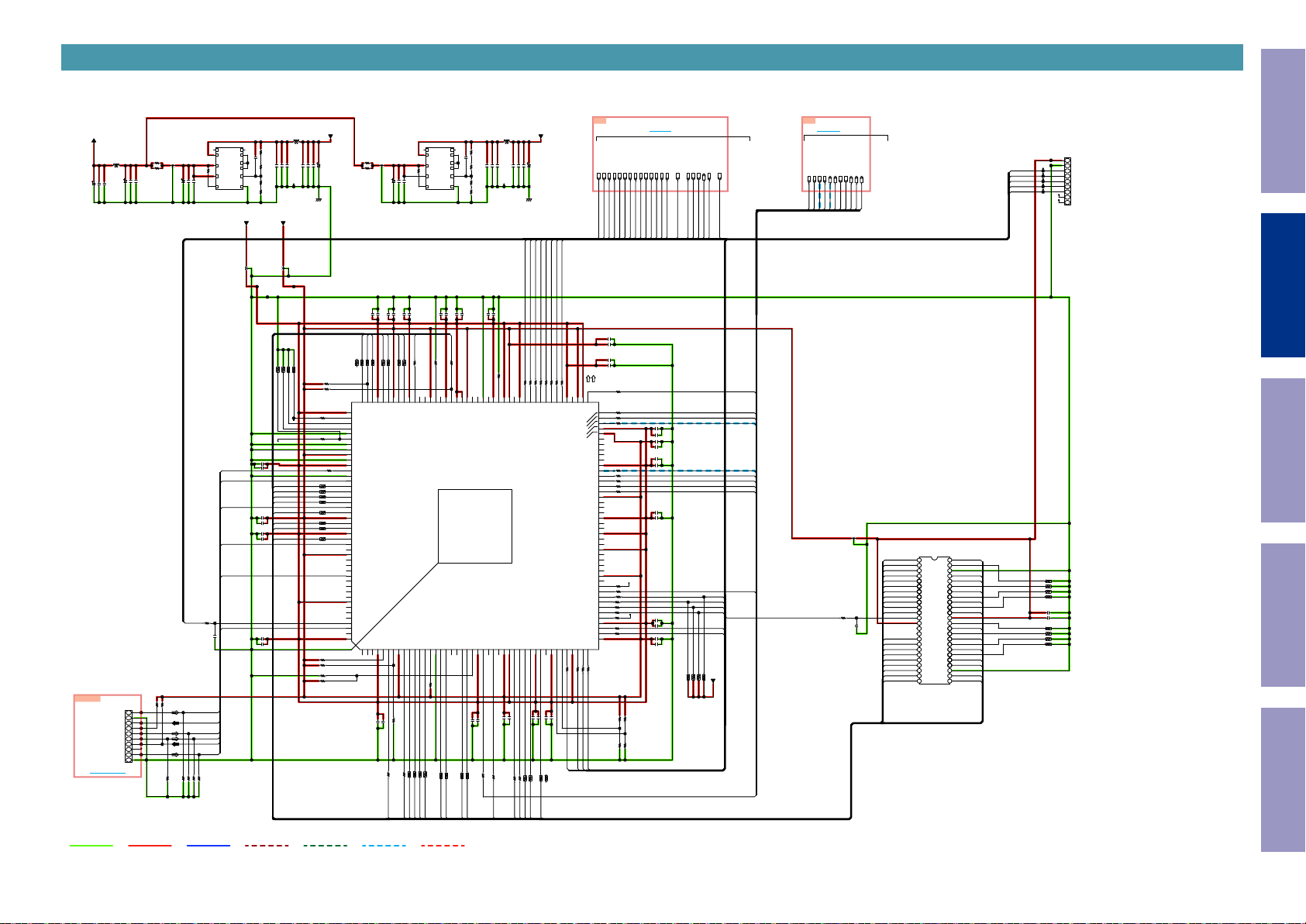
SCH10_DIGITAL(6/7)
All Ref.No. has been described in the parts list are four digits.
But there are less than four digits of printed Ref.No. on the PCB, and they have become four digits after the header by adding "0" in the parts list.
Caution in
servicing
C173
N101_
220/6.3
+5V_DSP
L106
BLM21PG221
0.1
0.01
C171
C172
10P-FFC
TO N102_
N101
TRST
EMU0
9A
to MCU
DSP_WL_1
DSP_FILT_0
OUTPUT
OUTPUT
DSP_WL_1
DSP_FILT_0
R140
R141
R142
R143
R144
R145
R146
R148
R147
R150
R151
R135
R136
R137
R190
R138
R139
TO A9
DSP_PHASE
DSP_DITH_1
DSP_FILT_3
DSP_FILT_2
DSP_SDM_1
DSP_SDM_0
DSP_DITH_0
DSP_FILT_1
INPUT
INPUT
INPUT
INPUT
INPUT
OUTPUT
OUTPUT
DSP_FILT_1
DSP_FILT_2
DSP_FILT_3
DSP_SDM_0
DSP_SDM_1
DSP_DITH_0
DSP_DITH_1
0.1
1000P
0.1
1000P
33
33
33
33
33
33
33
33
33
R149
OPEN
33
0
47
0
0
33
C142
C143
33
33
C144
C147
R154
R152
OPEN
OPEN
R153
R155
10K
10K
DSP_HOLD
DSP_HOLD
OUTPUT
1000P
DSP_DEEM
OUTPUT
OUTPUT
DSP_PHASE
DSP_DEEM
1000P
DSP1_CS
DSP_ROM_RST
DSP_RST
DSP_MOSI
DSP_CLK
DSP_MUTE
OUTPUT
DSP_MUTE
0.1
0.1
DSP2_CS
DSP_MISO
OUTPUT
OUTPUT
OUTPUT
OUTPUT
OUTPUT
OUTPUT
OUTPUT
DSP2_CS
DSP_CLK
DSP_MISO
DSP_MOSI
DSP1_CS
DSP_RST
DSP_ROM_RST
DSD_BCK.
DSD_LRCK.
DSPDSD_R.
C136
1000P
0.1
C145
1000P
C137
0.1
C146
0.1
C138
1000P
C139
0.1
C140
1000P
C141
4.7Kx4
1 2
R192
DSPDSD_L.
PLD_DATA_OUT.
PLD_LRCK_OUT.
PLD_BCK_OUT.
WDT_P1
CH_SYNC_1
DSP1_TEST_0
DSP_CLK
DSP_MISO
DSP_MOSI
DSP1_CS
DSP_ROM_RST
DSP_WL_0
DSP_WL_1
4.7Kx4
4.7Kx4
4.7Kx4
33_VCCIO
7 8
5 6
3 4
R192
R192
R192
24M_DSP1
L107
+1.1_VDSP_1
NC
1
NC
4
L2
11
10
1u
C158
OPEN
R106
0
R179
R108
0
DSP1TCK
DSP1TDO
DSP1TMS
DSP1TRST
DSP1EMU0
DSP1TDI
10K
R107
9
PVIN
7
AVIN
6
CE
U3007
XCL212B082DR
DSP1TRST
DSP1EMU0
DSP1TDO
DSP1TDI
DSP1TCK
DSP1TMS
OPEN
C101
FB
GND
C102
C103
C104
C105
C106
C109
C107
C108
L1
2
LX
3
LX
5
8
+1.1_VDSP_1
NFM18PS105R0J3
L101
1000P
1000P
1000P
1000P
1.8
NFM18PS105R0J3
R184
L102
1.8
0.1
0.01
R185
C170
220/6.3
C169
C168
TCK
1
GND
2
TDO
3
VCC
4
5
TMS
6
7
EMU1
8
TDI
9
GND
10
0.1
C157
220/6.3
C167
DSP_RST
R101
R102
OPEN
OPEN
10K
10K
4.7K
R104
R105
R103
BLM21PG221
R180
1000P
8.2K
0.01
0.1
10/6.3
10/6.3
10/6.3
1000P
C159
R181
10K
C165
C164
C163
C161
C160
C162
R182
47K
1K
R183
33_VCCIO
L103
NFM18PS105R0J3
4.7Kx4
3 4
R191
GND
4.7Kx4
4.7Kx4
4.7Kx4
1 2
7 8
5 6
R191
R191
R191
R157
R160
R109
R110
0.1
DSP1D0
R158
DSP1D1
R158
DSP1D2
R158
DSP1D3
R158
DSP1D4
R159
DSP1D5
DSP1D6
DSP1D7
R159
R159
R159
0.1
0.1
0.1
R112
R156
R113
R114
C166
220/6.3
-
OPEN
OPEN
133
VDD_INT
82
134
FLAGO
135
FLAG1
136
FLAG2
137
GND
138
OPEN
FLAG3
139
GND
140
GND
141
VDD_EXT
142
GND
143
VDD_INT
82
R111
144
TRST
145
GND
146
EMU
10x4
147
DATA0
1
2
10x4
148
DATA1
3
4
10x4
149
DATA2
5
6
10x4
150
DATA3
7
8
151
TDO
10x4
152
DATA4
1
2
153
Vdd?EXT
10x4
154
DATA5
3
4
10x4
155
DATA6
5
6
156
VDD_INT
10x4
157
DATA7
7
8
158
TDI
159
SDCLK
160
VDD_EXT
161
DATA8
162
DATA9
163
DATA10
164
TCK
165
DATA11
166
DATA12
167
DATA14
168
DATA13
169
VDD_INT
170
DATA 15
171
SDWE
172
SDRAS
173
RESET
174
TMS
175
SDCAS
176
VDD_INT
GND
177
4.7K
OPEN
4.7K
OPEN
1.8
NFM18PS105R0J3
R284
L202
1.8
0.1
R285
C184
220/6.3
C183
1000P
0.1
1000P
0.1
C111
C110
C115
C114
DSP1RD
DSP1A14
DSP1A15
DSP1A16
DSP1A19
DSP1WR
R115
R115
R115
R115
33x4
33x4
33x4
8
1234567
8
R165
R165
R165
33x4
33x4
33x4
33x4
125
126
127
128
129
130
131
132
ADDR19
VDD_EXT
ADDR16
ADDR15
VDD_INT
ADDR14
AMI_WR
AMI_RD
SDDQM2MSO3SDCKE4VDD_INT5CLK_CFG16ADDRO7BOOT_CFGO8VDD_EXT9ADDRl10ADDR211ADDR312ADDR413ADDR514BOOT_CFGl15GND16ADDR617ADDR7
1
R172
4.7K
0.1
1000P
C113
C112
R16633R167
DSP1A0
1u
C182
0.1
C116
DSP1A20
33x4
1234567
R165
124
ADDR20
33
DSP1A1
0
1000P
C117
123
VDD_INT
33x4
7 8
R161
DSP1A2
R279
DSP1A21
OPEN
R117
121
122
ADDR21
33x4
33x4
5 6
R161
R161
DSP1A4
DSP1A3
3 4
NC
1
NC
4
L2
11
10
L1
2
LX
9
PVIN
3
LX
7
5
AVIN
FB
GND
8
6
CE
U3008
XCL212B082DR
0.1
1000P
C119
C118
DSP1CE1
4.7K
R118
115
116
117
118
119
120
MS1
VDD_INT
WDT_CLKO
WDT_CLKIN
VDD_EXT
ADDR23
ADDR22
ADSP-21489KSWZ-4B
DSP1
18NC19NC20
R173
4.7K
33x4
33x4
33x4
1 2
5 6
7 8
R161
R162
R162
DSP1A7
DSP1A6
DSP1A5
L108
+1.1_VDSP_2
BLM21PG221
R280
1000P
8.2K
0.01
0.1
10/6.3
10/6.3
10/6.3
112
VDD_THD
1000P
R281
10K
C175
R282
47K
1K
R283
108
109
110
111
GND
THD_M
THD_P
C181
220/6.3
C180
C179
C178
C176
C177
-
GND
DSP_MUTE
DSP_DEEM
DSP_HOLD
DSP_SDM_1
DSP_SDM_0
DSP_PHASE
DSP_DITH_1
DSP_DITH_0
0.1
1000P
C125
C124
R174
33
33
33
33
33
AMI_ACK
107
VDD_INT
4.7K
103
104
105
106
VDD_EXT
VDD_INT
B00T_CFG2
R12333R129
R124
100
101
102
DAI_P12
DAI_P15
VDD_INT
DAI_P11
R12533R12633R127
R130
R128
1000P
C120
33
R119
114
VDD_INT
C174
0.1
C121
113
VDD_INT
U101
ADDR821ADDR922CLK_CFGO23VDD_INT24CLKIN25XTAL26ADDRIO27SDA1028VDD_EXT29VDD_INT30ADDRll31ADDR1232ADDR1733ADDR1334VDD_INT35ADDR1836RESETOUT/RUNRSTIN37VDD_INT38DPI_P0139DPI_P0240DPI_P0341VDD_INT42DPI_P0543DPI_P0444DPI_P06
0.1
1000P
0.1
1000P
C126
C127
C123
C122
33x4
33x4
56
33
33x4
33
3 4
1 2
R162
R162
DSP1A9
DSP1A8
33
7856341
R120
R168
R164
R170
R169
DSP1A17
DSP1A10
DSP1A11
DSP1A12
1000P
C128
33x4
R164
DSP1A13
0.1
C129
33x4
R164
DSP1A18
R131
33
0.1
1000P
C131
C130
DSP_FILT_3
DSP_FILT_0
33x4
2
R164
DSP_FILT_1
89
DAI_P09
DAI_P1090VDD_INT91VDD_EXT92DAI_P2093VDD_INT94DAI_P0895DAI_P1496DAI_P0497DAI_P1898DAI_P1799DAI_P16
DAI_P05
DAI_P06
VDD_INT
VDD_EXT
NC
NC
NC
NC
NC
VDD_INT
DAI_P02
DAI_P01
DAI_P19
DAI_P13
DAI_P07
VDD_EXT
NC
WDTRSTO
NC
VDD_INT
NC
NC
VDD_INT
NC
NC
VDD_INT
NC
NC
NC
NC
VDD_EXT
NC
DAI_P03
DPI_P14
DPI_P13
DPI_P12
DPI_P11
DPI_P10
DPI_P09
VDD_INT
DPI_P07
DPI_P08
VDD_EXT
DSP_FILT_2
R13433R13233R133
33
DSP_WL_0
OUTPUT
DSP_WL_0
C132
C133
C134
C135
88
87
86
85
84
83
82
81
80
79
78
77
76
75
74
73
72
71
70
69
68
67
66
65
64
63
62
61
60
59
58
57
56
55
54
53
52
51
50
49
48
47
46
45
3C
24M_DSP1
24M_DSP1
OUTPUT
OUTPUT
PLD_LRCK_OUT.
TO C3
PL D_L RC K_ OUT.
PLD_BCK_OUT.
PL D_D ATA _O UT.
OUTPUT
OUTPUT
PLD_DATA_OUT.
PLD_BCK_OUT.
DSPDSD_R.
DSPDSD_L.
INPUT
INPUT
DSPDSD_L.
DSPDSD_R.
R193
to PLD
DSD_BCK.
OUTPUT
DSD_BCK.
DSD_LRCK.
DSP1_TEST_0
INPUT
OUTPUT
DSD_LRCK.
DSP1_TEST_0
L105
NFM18PS105R0J3
0
0.1
C148
CH_SYNC_1
INPUT
CH_SYNC_1
WDT_P1
N402
9P-FFC
1
DSP_CLK
WDT_P1
INPUT
DSP_MOSI
DSP_MISO
DSP1_CS
DSP2_CSDSP2_CS
2
3
4
5
6
7
8
9
Electrical Mechanical Repair Information Updating
DSP1A16
DSP1A15
DSP1A14
DSP1A13
DSP1A12
DSP1A11
DSP1A10
DSP1A9
DSP1A20
DSP1A21
DSP1WR
DSP1A19
DSP1A18
DSP1A8
DSP1A7
DSP1A6
DSP1A5
DSP1A4
DSP1A3
DSP1A2
A15
1
A14
2
A13
3
A12
4
A11
5
A10
6
A9
7
A8
8
A19
9
NC
10
WE
11
RST
12
NC
13
NC
14
RY/BY
15
A18
16
A17
17
A7
18
A6
19
A5
20
A4
21
A3
22
A2
23
A1
24
MX29LV160DBTI-70G
U102
DQ15/A-1
DSP1A17
A16
48
BYTE
47
VSS
46
DSP1A0
45
DSP1D7
DQ7
44
DQ14
43
DSP1D6
DQ6
42
DQ13
41
DSP1D5
DQ5
40
DQ12
39
DSP1D4
DQ4
38
VCC
37
DQ11
36
DSP1D3
DQ3
35
DQ10
34
DSP1D2
DQ2
33
DQ9
32
DSP1D1
DQ1
31
DQ8
30
DSP1D0
DQ0
29
DSP1RD
OE
28
VSS
27
DSP1CE1
CE
26
DSP1A1
A0
25
4.7Kx4
R121
7 8
R121
4.7Kx4
5 6
4.7Kx4
R121
3 4
R121
4.7Kx4
1 2
1000P
C149
0.1
C150
4.7Kx4
R122
7 8
4.7Kx4
R122
5 6
4.7Kx4
R122
3 4
4.7Kx4
R122
1 2
DSP1
GND LINE
POWER+ LINE
POWER- LINE
ANALOG AUDIO R ANALOG AUDIO L
DIGITAL AUDIO
STBY POWER
18
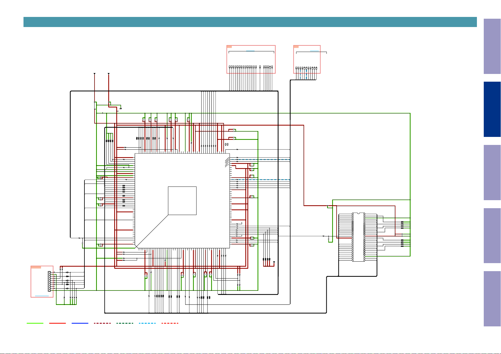
SCH11_DIGITAL(7/7)
All Ref.No. has been described in the parts list are four digits.
But there are less than four digits of printed Ref.No. on the PCB, and they have become four digits after the header by adding "0" in the parts list.
Caution in
servicing
N102_
TO N101_
10P-FFC
N102
TRST
EMU0
to MCU
8A
33_VCCIO
+1.1_VDSP_2
DSP_MUTE
DSP_DEEM
DSP_HOLD
DSP_SDM_1
DSP_SDM_0
DSP_PHASE
DSP_DITH_1
105
VDD_INT
104
C227
VDD_EXT
102
103
DAI_P11
1000P
33
33
R270
R269
.DSP1A11
.DSP1A12
33
101
VDD_INT
33x4
7856341
R264
.DSP1A17
R22333R22433R22533R22833R22633R227
R25633R255
100
DAI_P12
DAI_P15
1000P
C228
33x4
R264
.DSP1A13
0.1
C229
33x4
R264
.DSP1A18
DSP_DITH_0
0.1
1000P
C231
C230
33x4
2
R264
33
89
DAI_P09
DAI_P1090VDD_INT91VDD_EXT92DAI_P2093VDD_INT94DAI_P0895DAI_P1496DAI_P0497DAI_P1898DAI_P1799DAI_P16
DAI_P05
DAI_P06
VDD_INT
VDD_EXT
NC
NC
NC
NC
NC
VDD_INT
DAI_P02
DAI_P01
DAI_P19
DAI_P13
DAI_P07
VDD_EXT
NC
WDTRSTO
NC
VDD_INT
NC
NC
VDD_INT
NC
NC
VDD_INT
NC
NC
NC
NC
VDD_EXT
NC
DAI_P03
DPI_P14
DPI_P13
DPI_P12
DPI_P11
DPI_P10
DPI_P09
VDD_INT
DPI_P07
DPI_P08
VDD_EXT
R231
R230
R232
R229
33
33
33
33
DSP_FILT_3
DSP_FILT_0
DSP_FILT_1
DSP_FILT_2
NFM18PS105R0J3
L201
L203
NFM18PS105R0J3
-
GND
DSP1.1V..
4.7Kx4
4.7Kx4
4.7Kx4
4.7Kx4
5 6
3 4
1 2
7 8
R291
R291
R291
R291
OPEN
R257
OPEN
R260
133
VDD_INT
82
R209
134
FLAGO
135
FLAG1
136
FLAG2
137
GND
138
R210
OPEN
FLAG3
139
GND
140
GND
141
VDD_EXT
142
C202
1000P
DSP2TRST
C203
0.1
DSP2EMU0
DSP2TDO
DSP2TDI
DSP2TCK
DSP_RST
R208
0
DSP2TMS
OPEN
C201
R201
R202
OPEN
OPEN
TCK
1
GND
2
TDO
3
VCC
4
5
TMS
6
7
EMU1
8
TDI
9
GND
10
DSP2TCK
DSP2TDO
DSP2TMS
DSP2TRST
DSP2EMU0
DSP2TDI
10K
10K
10K
OPEN
4.7K
R204
R205
R206
R207
R203
.DSP1D0
.DSP1D1
.DSP1D2
.DSP1D3
.DSP1D4
C204
1000P
.DSP1D5
0.1
C205
.DSP1D6
C206
1000P
.DSP1D7
C209
0.1
C207
1000P
C208
0.1
GND
143
VDD_INT
82
R211
144
TRST
145
GND
146
EMU
10x4
R258
147
DATA0
1
2
10x4
R258
148
DATA1
3
4
10x4
149
R258
DATA2
5
6
R258
10x4
150
DATA3
7
8
151
TDO
10x4
R259
152
DATA4
1
2
153
Vdd?EXT
10x4
154
R259
DATA5
3
4
10x4
155
R259
DATA6
5
6
156
VDD_INT
10x4
R259
157
DATA7
7
8
158
TDI
159
SDCLK
160
VDD_EXT
161
DATA8
162
DATA9
163
DATA10
164
TCK
165
DATA11
166
DATA12
167
DATA14
168
DATA13
169
VDD_INT
170
DATA 15
171
SDWE
172
SDRAS
173
RESET
174
TMS
175
SDCAS
176
VDD_INT
GND
177
4.7K
R212
OPEN
R263
4.7K
R213
OPEN
R214
0.1
1000P
0.1
1000P
1000P
.DSP1RD
R215
1234567
33x4
132
AMI_RD
0.1
C210
.DSP1A14
.DSP1WR
R215
33x4
33x4
130
131
AMI_WR
C211
R215
8
129
ADDR14
.DSP1A15
R215
R265
33x4
VDD_INT
33x4
8
128
ADDR15
C215
C214
.DSP1A16
33x4
R265
126
127
ADDR16
.DSP1A19
33x4
R265
125
VDD_EXT
C216
.DSP1A20
1234567
R265
124
ADDR19
33x4
ADDR20
C217
123
VDD_INT
.DSP1A21
OPEN
R217
121
122
ADDR21
120
ADDR22
119
ADDR23
0.1
C218
4.7K
R218
117
118
WDT_CLKO
WDT_CLKIN
VDD_EXT
ADSP-21489KSWZ-4B
SDDQM2MSO3SDCKE4VDD_INT5CLK_CFG16ADDRO7BOOT_CFGO8VDD_EXT9ADDRl10ADDR211ADDR312ADDR413ADDR514BOOT_CFGl15GND16ADDR617ADDR7
1
R273
4.7K
R272
4.7K
0.1
1000P
C213
C212
33x4
33x4
33x4
33x4
R26733R266
.DSP1A1
7 8
R261
.DSP1A2
5 6
R261
.DSP1A3
3 4
R261
.DSP1A4
1 2
R261
.DSP1A5
33x4
7 8
R262
.DSP1A6
33
.DSP1A0
0.1
1000P
1000P
0.1
1000P
C219
C221
C220
C225
C224
.DSP1CE1
116
VDD_INT
33
R219
115
MS1
114
VDD_INT
113
VDD_INT
112
VDD_THD
R274
4.7K
106
107
108
109
110
111
GND
B00T_CFG2
VDD_INT
AMI_ACK
THD_M
THD_P
U201
DSP2
ADDR821ADDR922CLK_CFGO23VDD_INT24CLKIN25XTAL26ADDRIO27SDA1028VDD_EXT29VDD_INT30ADDRll31ADDR1232ADDR1733ADDR1334VDD_INT35ADDR1836RESETOUT/RUNRSTIN37VDD_INT38DPI_P0139DPI_P0240DPI_P0341VDD_INT42DPI_P0543DPI_P0444DPI_P06
18NC19NC20
0.1
0.1
1000P
C226
C223
C222
33x4
33x4
33x4
56
33
5 6
3 4
1 2
R220
R262
R262
R262
R268
.DSP1A7
.DSP1A9
.DSP1A8
.DSP1A10
DSP_WL_0
OUTPUT
OUTPUT
DSP_WL_0
DSP_WL_1
C232
C233
C234
C235
88
87
86
85
84
83
82
81
80
79
78
77
76
75
74
73
72
71
70
69
68
67
66
65
64
63
62
61
60
59
58
57
56
55
54
53
52
R233
51
R234
50
R235
49
R287
48
47
R236
46
R237
45
DSP_WL_1
DSP_FILT_0
OUTPUT
DSP_FILT_0
DSP_FILT_1
R238
R239
R240
R241
R242
R243
R244
R246
R245
OPEN
R248
R249
DSP_FILT_1
INPUT
DSP_FILT_2
0.1
1000P
0.1
1000P
R247
TO A8
DSP_PHASE
DSP_DITH_1
DSP_FILT_3
DSP_FILT_2
DSP_SDM_1
DSP_SDM_0
DSP_DITH_0
INPUT
INPUT
INPUT
INPUT
OUTPUT
OUTPUT
DSP_FILT_3
DSP_SDM_0
DSP_SDM_1
DSP_DITH_0
DSP_DITH_1
33
33
33
33
33
33
33
33
33
33
0
47
0
0
33
C242
C243
33
33
C244
C247
R250
R252
OPEN
10K
R251
R253
10K
OPEN
DSP_HOLD
DSP_HOLD
OUTPUT
1000P
DSP_DEEM
OUTPUT
OUTPUT
DSP_PHASE
DSP_DEEM
1000P
DSP2_CS
DSP_ROM_RST
DSP_RST
DSP_MOSI
DSP_CLK
DSP_MUTE
DSP_MISO
OUTPUT
OUTPUT
OUTPUT
OUTPUT
OUTPUT
OUTPUT
OUTPUT
DSP_CLK
DSP_MISO
DSP_MOSI
DSP2_CS
DSP_RST
DSP_ROM_RST
DSP_MUTE
C236
1000P
0.1
C245
1000P
C237
0.1
C246
0.1
C238
1000P
C239
0.1
C240
1000P
C241
DSP_CLK
DSP_MISO
DSP_MOSI
DSP2_CS
DSP_WL_0
0.1
DSP_WL_1
0.1
4.7Kx4
4.7Kx4
4.7Kx4
4.7Kx4
1 2
7 8
3 4
5 6
33_VCCIO
R292
R292
R292
R292
DSD_LRCK..
DSPDSD_R..
DSPDSD_L..
PLD_DATA_OUT..
PLD_LRCK_OUT..
PLD_BCK_OUT..
CH_SYNC_2
DSP2_TEST_0
DSP_ROM_RST
24M_DSP2
DSD_BCK..
WDT_P2
4C
OUTPUT
24M_DSP2
24M_DSP2
TO C4
to PLD
DSD_BCK..
DSD_LRCK..
PL D_L RC K_ OUT. .
PLD_BCK_OUT..
PL D_D ATA _O UT. .
DSPDSD_R..
DSP2_TEST_0
CH_SYNC_2
WDT_P2
DSPDSD_L..
INPUT
INPUT
INPUT
INPUT
INPUT
OUTPUT
OUTPUT
OUTPUT
OUTPUT
OUTPUT
PLD_LRCK_OUT..
PLD_DATA_OUT..
PLD_BCK_OUT..
DSPDSD_L..
DSPDSD_R..
DSD_BCK..
DSD_LRCK..
DSP2_TEST_0
CH_SYNC_2
WDT_P2
Electrical Mechanical Repair Information Updating
L205
NFM18PS105R0J3
.DSP1A16
1
.DSP1A15
2
.DSP1A14
3
.DSP1A13
4
.DSP1A12
5
.DSP1A11
6
.DSP1A10
7
.DSP1A9
8
.DSP1A20
9
.DSP1A21
10
.DSP1WR
.DSP1A19
.DSP1A18
.DSP1A8
.DSP1A7
.DSP1A6
.DSP1A5
.DSP1A4
.DSP1A3
.DSP1A2
11
12
13
14
15
16
17
18
19
20
21
22
23
24
MX29LV160DBTI-70G
R293
0
0.1
C248
.DSP1A17
A16
A15
48
BYTE
A14
47
VSS
A13
46
U202
DQ15/A-1
.DSP1A0
45
.DSP1D7
DQ7
44
DQ14
43
.DSP1D6
DQ6
42
DQ13
41
.DSP1D5
DQ5
40
DQ12
39
.DSP1D4
DQ4
38
VCC
37
DQ11
36
.DSP1D3
DQ3
35
DQ10
34
.DSP1D2
DQ2
33
DQ9
32
.DSP1D1
DQ1
31
DQ8
30
.DSP1D0
DQ0
29
.DSP1RD
OE
28
VSS
27
.DSP1CE1
CE
26
.DSP1A1
A0
25
4.7Kx4
R221
7 8
R221
4.7Kx4
5 6
4.7Kx4
R221
3 4
R221
4.7Kx4
1 2
1000P
C249
0.1
C250
4.7Kx4
R222
7 8
4.7Kx4
R222
5 6
4.7Kx4
R222
3 4
4.7Kx4
R222
1 2
A12
A11
A10
A9
A8
A19
NC
WE
RST
NC
NC
RY/BY
A18
A17
A7
A6
A5
A4
A3
A2
A1
DSP2
GND LINE
POWER+ LINE
POWER- LINE
ANALOG AUDIO R ANALOG AUDIO L
DIGITAL AUDIO
STBY POWER
19
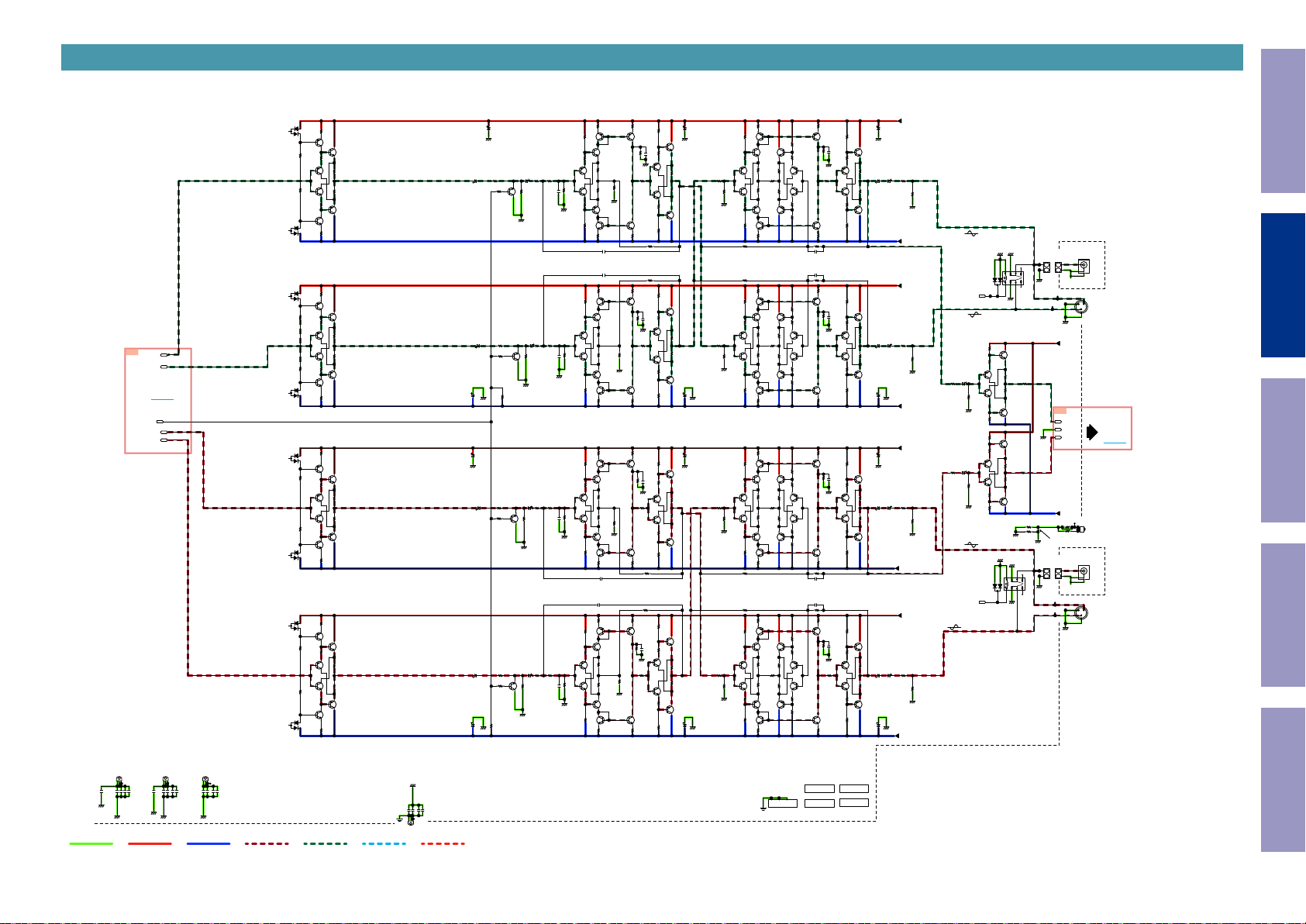
SCH12_AUDIO(1/4)
All Ref.No. has been described in the parts list are four digits.
But there are less than four digits of printed Ref.No. on the PCB, and they have become four digits after the header by adding "0" in the parts list.
Caution in
servicing
POST FILTER/BALANCE
C5
L_+
L_-
TO 5C
MUTE_TR
R_+
R_-
D7952
KDS122
1
R7317
L-
R7319
D7953
KDS122
1
D7954
KDS122
1
R7318
L+
R7320
D7955
KDS122
1
D7956
KDS122
1
R7517
R-
R7519
D7957
KDS122
1
D7958
KDS122
1
R7518
R+
R7520
D7959
KDS122
1
77kHz 2nd order LPF
2
R7301
3
470
2SA1312(B)
Q7309
Q7305
R7303
33K
2SC3324
47
2SA1312(B)
Q7301
R7309
22
33K
R7311
22
Q7303
2SC3324
R7305
47
Q7307
2SA1312(B)
2
Q7311
2SC3324
3
R7307
470
2
470
R7302
3
2SA1312(B)
Q7310
33K
Q7306
2SC3324
R7304
47
2SA1312(B)
Q7302
R7310
22
R7312
22
Q7304
2SC3324
33K
R7306
47
Q7308
2SA1312(B)
2
Q7312
2SC3324
3
470
R7308
470
R7501
2
3
2SA1312(B)
Q7509
33K
Q7505
2SC3324
R7503
47
2SA1312(B)
Q7501
R7509
22
R7511
22
Q7503
2SC3324
33K
R7505
47
Q7507
2SA1312(B)
2
Q7511
2SC3324
3
470
R7507
2
470
R7502
3
2SA1312(B)
Q7510
33K
Q7506
2SC3324
R7504
47
2SA1312(B)
Q7502
R7510
22
R7512
22
33K
Q7504
2SC3324
R7506
47
Q7508
2SA1312(B)
2
Q7512
3
2SC3324
470
R7508
C7309
470/25
AGND
C7305
47/25
C7306
47/25
C7312
AGND
470/25
C7509
470/25
AGND
C7505
47/25
C7506
47/25
C7512
AGND
470/25
3.32K
R7349
C7307
R7433
47/25
46.4
R7431
4.7K
100K
R7347
Q7375
KTC2875B
AGND
C7308
R7434
3.32K
47/25
46.4
R7432
4.7K
100K
R7348
Q7376
KTC2875B
AGND
470K
R7499
C7507
R7549
47/25
R7633
3.32K
46.4
R7631
4.7K
100K
R7547
Q7575
KTC2875B
AGND
C7508
R7634
47/25
3.32K
46.4
R7632
4.7K
100K
R7548
Q7576
KTC2875B
AGND
470K
R7699
R7355
15K
R7357
47
1.62K
R7351
2SA1312(B)
Q7331
R7353
C7313
47K
Q7333
1000P
2SC3324
R7359
47
AGND
R7361
15K
R7356
R7350
R7550
R7358
2SA1312(B)
Q7332
R7352
1.62K
1000P
C7314
47K
Q7334
2SC3324
R7360
R7354
AGND
R7362
R7555
R7557
2SA1312(B)
R7551
Q7531
1.62K
C7513
1000P
R7553
47K
Q7533
2SC3324
R7559
AGND
R7561
R7556
R7558
2SA1312(B)
Q7532
R7552
1.62K
C7514
1000P
R7554
47K
Q7534
2SC3324
R7560
AGND
R7562
150
R7363
R7371
470
Q7339
2SA1312(B)
Q7335
2SC3324
22
R7365
22
R7822
R7367
820
AGND
Q7337
2SA1312(B)
Q7341
2SC3324
470
150
R7369
R7373
C7315
1000P
C7316
1000P
150
R7364
470
R7372
Q7340
15K
2SA1312(B)
Q7336
2SC3324
R7376
47
22
R7366
22
820
R7823
R7368
47
AGND
Q7338
2SA1312(B)
Q7342
15K
2SC3324
470
150
R7370
R7374
150
R7563
R7571
470
Q7539
15K
2SA1312(B)
Q7535
R7575
2SC3324
47
22
R7565
22
R7567
820
R7824
47
AGND
Q7537
2SA1312(B)
Q7541
15K
2SC3324
150
R7569
R7573
470
C7515
1000P
C7516
1000P
150
R7564
470
R7572
Q7540
15K
2SA1312(B)
Q7536
2SC3324
47
R7576
22
R7566
R7825
22
R7568
820
AGND
47
Q7538
2SA1312(B)
Q7542
15K
2SC3324
470
150
R7570
R7574
C7319
R7460
15K
470/25
Q7343
2SC3324
Q7347
AGND
2SA1312(B)
47
1M
330P
C7317
R7461
R7375
AGND
2SA1312(B)
R7462
46.4
Q7387
47
Q7388
R7463
2SC3324
Q7345
2SC3324
R7464
Q7349
15K
2SA1312(B)
R7818
464
R7819
464
R7470
15K
Q7344
2SC3324
Q7348
2SA1312(B)
47
R7471
330P
1M
C7318
AGND
R7472
2SA1312(B)
46.4
Q7391
47
Q7392
2SC3324
R7473
Q7346
Q7350
2SC3324
R7474
15K
2SA1312(B)
R7640
Q7543
15K
Q7547
2SC3324
2SA1312(B)
47
330P
C7517
1M
R7641
AGND
R7642
2SA1312(B)
46.4
Q7815
Q7816
47
R7643
2SC3324
R7644
Q7545
15K
2SC3324
Q7549
2SA1312(B)
R7820
464
R7821
464
R7650
15K
Q7544
2SC3324
Q7548
2SA1312(B)
47
330P
C7518
R7651
1M
AGND
2SA1312(B)
R7652
46.4
Q7819
47
Q7820
2SC3324
R7653
Q7546
Q7550
2SC3324
R7654
15K
2SA1312(B)
R7381
R7377
22
1K
R7379
22
R7382
22
R7378
1K
R7380
22
C7322
AGND
470/25
C7519
470/25
AGND
R7581
R7577
22
1K
R7579
22
R7583
R7582
22
R7578
1K
R7580
22
R7584
C7522
AGND
470/25
R7395
470
Q7359
R7387
15K
2SA1312(B)
Q7355
2SC3324
R7389
47
22
2SA1312(B)
Q7351
R7397
R7429
22
R7399
1K
R7383
Q7353
2SC3324
R7391
AGND
47
Q7357
2SA1312(B)
Q7361
R7393
15K
2SC3324
470
R7401
R7385
3.01K
R7386
3.01K
R7396
470
Q7360
R7388
15K
2SA1312(B)
Q7356
2SC3324
R7390
47
22
R7398
2SA1312(B)
Q7352
R7430
22
R7400
1K
R7384
Q7354
AGNDAGND
2SC3324
R7392
AGND
47
Q7358
2SA1312(B)
Q7362
R7394
15K
2SC3324
470
R7402
R7595
470
Q7559
R7587
15K
2SA1312(B)
Q7555
2SC3324
R7589
47
22
2SA1312(B)
R7597
Q7551
R7729
100
Q7553
Q7552
Q7554
2SC3324
2SA1312(B)
2SC3324
22
R7599
R7591
47
Q7557
2SA1312(B)
Q7561
R7593
15K
2SC3324
R7601
470
R7585
3.01K
R7586
3.01K
R7596
470
Q7560
R7588
15K
2SA1312(B)
Q7556
2SC3324
R7590
47
22
R7598
R7730
22
R7600
R7592
47
Q7558
2SA1312(B)
Q7562
R7594
15K
2SC3324
R7602
470
1K
AGND
1K
AGND
2SC3324
R7451
100
R7453
2SA1312(B)
2SC3324
R7452
100
R7454
2SA1312(B)
2SC3324
R7751
R7753
2SA1312(B)
2SC3324
R7752
100
R7754
2SA1312(B)
150
R7405
R7411
Q7363
15K
2SA1312(B)
R7443
330P
15K
Q7381
22
22
Q7383
Q7382
22
22
Q7384
Q7681
22
22
Q7683
Q7682
22
22
Q7684
C7325
220K
R7409
47
R7445
47
R7447
47
R7446
47
R7448
47
R7745
47
R7747
47
R7746
47
R7748
R7413
47
Q7367
2SA1312(B)
Q7377
AGND
2SA1312(B)
R7810
46.4
Q7369
2SC3324
Q7379
2SC3324
R7415
47
15K
R7449
R7417
15K
Q7365
2SC3324
150
R7407
3.01K
R7403
C7323
10P
10P
C7324
R7404 3.01K
150
R7406
R7412
Q7364
15K
2SA1312(B)
R7444
15K
330P
C7326
220K
R7410
R7414
47
Q7368
2SA1312(B)
Q7378
AGND
2SA1312(B)
R7811
46.4
Q7370
Q7380
2SC3324
2SC3324
R7416
47
R7450
15K
R7418
15K
Q7366
2SC3324
150
R7408
150
R7605
R7611
Q7563
15K
2SA1312(B)
15K
R7743
330P
C7525
220K
R7609
R7613
47
Q7677
Q7567
2SA1312(B)
AGND
2SA1312(B)
R7812
46.4
Q7569
Q7679
2SC3324
2SC3324
R7615
47
15K
R7749
R7617
15K
Q7565
2SC3324
150
R7607
R7603
3.01K
C7523
10P
10P
C7524
R7604 3.01K
150
R7606
R7612
Q7564
15K
15K
2SA1312(B)
R7744
330P
C7526
R7610
220K
R7614
47
Q7678
Q7568
2SA1312(B)
AGND
2SA1312(B)
R7813
46.4
Q7570
Q7680
2SC3324
2SC3324
R7616
R7750
47
15K
R7618
15K
Q7566
2SC3324
150
R7608
+15V-15V
C7329
470/25
AGND
Q7371
2SC3324
R7423
C7333
46.4
220/16
R7419
22
C7327
220/16
R7421
22
R7425
100K
AGND
Q7373
2SA1312(B)
AGND..
AGND
S7055
G6K-2P-Y
817 6 5
2
3
D7055
2 3 4
1
+15V-15V
Q7372
2SC3324
C7334
22
R7424
220/16
R7420
46.4
C7328
220/16
22
R7422
Q7374
Q7571
2SC3324
R7619
22
R7621
Q7573
Q7572
2SC3324
R7620
22
R7622
Q7574
2SA1312(B)
C7332
470/25
C7529
470/25
AGND
C7527
220/16
22
2SA1312(B)
C7528
220/16
22
2SA1312(B)
C7532
470/25
220/16
220/16
R7426
100K
AGND
AGND
+15V
C7533
R7623
46.4
R7625
100K
AGND
-15V
+15V
R7624
C7534
46.4
R7626
100K
AGND
AGND
-15V
1SS301
M_RELAY
AGND
R7703
15K
Q7703
2SC3324
R7704
Q7701
47
2SA1312(B)
C7701
47/25
100
R7701
47/25
R7801
100
R7707
22
R7709
100
22
R7708
Q7702
10K
R7702
2SC3324
R7705
47
AGND
Q7704
2SA1312(B)
R7706
15K
R7803
15K
Q7803
2SC3324
Q7801
R7804
47
2SA1312(B)
C7801
R7802
10K
2SC3324
AGND
M_RELAY
R7809
22
100
R7807
22
R7808
Q7802
(B)
R7805
47
Q7804
2SA1312(B)
R7806
15K
R7853
0
R7855
AGND..
0
内層プレーン
AGND..
AGND
S7951
G6K-2P-Y
AGNDAGND
AGND..
817 6 5
2
3
D7951
3 4
2
1
1SS301
AGND
2P-EH
AGND
AGND
2P-EH
AGND
N7003
121
AGND
+15V,-15VのもとGND
N7004
2
W7902
EHR2-BARA
2
AGND
+15V
C6
L_BUFOUT
R_BUFOUT
-15V
C7901
OPEN
C7902
OPEN
W7952
EHR2-BARA
121
AGND
K7902
1P_RCA_JACK
L-CH
1
2
3
K7901
3P-CANNON
HEADPHONE
CIRCUIT
AGND
TO 6C
4
B7002
3
2
M3-SIDE
1
K7952
1P_RCA_JACK
R-CH
(基板外)
1
2
3
K7951
3P-CANNON
Electrical Mechanical Repair Information Updating
C6001
GND LINE
GND-TERMINAL
0.1
AGND..
B6001
0.1
C6061
1000P
C6002
AGND
0.1
100P
C6035
C6036
0.01
C6021
AGND..
POWER+ LINE
C6006
0.1
AGND
GND-TERMINAL
C6007
1000P
B6002
C6037
100P
C6016
C6038
0.01
POWER- LINE
B6004
GND-TERMINAL
OPEN
OPEN
C6040
OPEN
C6017
OPEN
C6039
AGND
ANALOG AUDIO R ANALOG AUDIO L
FG2
DIGITAL AUDIO
AGND
1000P
C7208
0.01
0.1
C7064
C7209
100P
C7065
B7201
GND-TERMINAL
STBY POWER
20
Z7008
WIRE_CLIP(01562-21)
65101001140AS
FG10
Z7003
Z7004
OPEN
OPEN
Z7002
Z7005
STYLE-PIN
OPEN
50mm
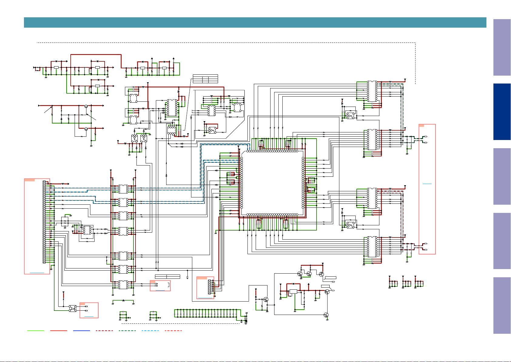
SCH13_AUDIO(2/4)
DISCRETE DAC
D7051
KDS160
+8VREG
0.1
C7003
470
R7070
UDZS5.6B
L7003
BLM21PG221
R7011
0
0
0
0
0
0
OPEN
L7009
L7010
OPEN
+3.3VD
OPEN
R7854
470/25
C7021
+3.3VD
GND
+3.3VD
TO A.POWER SHEET
4
3
0.1
C7001
0.1
C7053
100/25
GND
R7017
47
R7018
47
GND
C7063
C7062
0.01
1000P
SEL_44/48.
HPGAIN_HI.
HPGAIN_MID.
U7018
TLP185
A
C
1
2
E
K
POWER- LINE
NFM2012P13C105F
L7002
2
33/16
C7002
NFM2012P13C105F
L7007
2
C7054
33/16
Q7001
2SC4883(O/Y)
R7066
22
Q7002
2SC4883(O/Y)
R7067
22
5
2A
6
1Y
7
VCC
8
TC7WHU04FU
U7022
R7075
R7074
PLD_FILTER.
C7
BIDIRECT
BIDIRECT
TO 7C
U7006
NFM2012P13C105F
R7077
L7008
NJM7808FA
OPEN
IN
OUT
13
+10V
2
R7076
+8V
The purpose of "DSDLN" which is inverted "DSDL" is to cancel return current of ground line.
N7005
33_VCCIO
33_VCCIO
DSDL
DSDLN
DSDR
DSDRN
DSDBCK
DIRMCK
22M_OUT
24M_OUT
GND
PLD_FILTER
SEL_44/48
H.P ON/OFF
VOLT_PROT_A
HPGAIN_HI
HPGAIN_MID
TO N4001
GND LINE
0.1
C7097
C7096
100/25
C7098
0
AGND
8.5V
C7008
100/25
D8101
40
39
38
GND
37
36
GND
GND
GND
GND
GND
GND
GND
GND
GND
GND
GND
GND
MUTE
GND
40P-FFC
35
34
33
32
31
30
29
28
27
26
25
24
23
22
21
20
19
18
17
16
15
14
13
12
11
10
N7005
R7012
R7013
R7014
R7015
R7016
9
8
7
6
5
4
3
2
1
GND
POWER+ LINE
D7052
KDS160
U7003
NJM2845DL1-33
IN
OUT
13
0.1
0.01
0.01
AGND
1M
1M
NJM2845DL1-33
C7024
3
2
1
C7005
IN
C7056
100/25
DIRMCK.
DSDBCK.
0.1
C7025
C7060
1000P
C7061
1000P
D7053
KDS160
U7021
5.6V
100/25
DSDL.
DSDLN.
0.01
C7034
C7948
220/6.3
AGND
OUT
0.01
C7949
C7057
220/6.3
AGND
+5VA2
+5VA1
+3.3VD
C7004
DSDR.
DSDRN.
R7005
680
R7006
680
10K
R7078
GND
GND
C7105
C7106
C7107
C7014
13
C7055
GND43Y
3A
2Y
1A
MUTE.
VOLT_PROT_1
VOLT_PROT_2
ANALOG AUDIO R ANALOG AUDIO L
+3.3X
+3.3DA_I
33/16
C7011
0.1
C7015
0.1
C7016
0.1
C7018
0.1
C7019
0.1
C7020
0.1
C7051
0.1
+3.3X
U7002
ADuM1285CRZ
VDD1
1
VIA
2
VIB
3
GND1
4
U7004
ADuM1285CRZ
VDD1
1
VIA
2
VIB
3
GND1
4
U7005
ADuM1285CRZ
VDD1
1
VIA
2
VIB
3
GND1
4
U7009
ADuM1285CRZ
GND2
5
VOB
6
VOA
7
VDD2
8
U7007
ADuM1280ARZ
VDD1
1
VIA
2
VIB
3
GND1
4
U7008
ADuM1280ARZ
VDD1
1
VIA
2
VIB
3
GND1
4
U7020
ADuM1280ARZ
VDD1
1
VIA
2
VIB
3
GND1
4
L7004
OPEN
OPEN
OPEN
NFM2012P13C105F
L7113
C7088
100/16
AGND
R7056
C7036
C7904
1
2
45.1584MHz
R7020
C7035
C7903
1
2
49.152MHz
AGND
U7102
TC7SGU04FE
L7109
11A121
0.1
C7926
AGND
C7030
0.1
VDD2
8
VOA
7
VOB
6
GND2
5
C7031
0.1
VDD2
8
VOA
7
VOB
6
GND2
5
C7032
0.1
VDD2
8
VOA
7
VOB
6
GND2
5
C7027
0.1
GND1
4
VIB
3
VIA
2
VDD1
1
C7028
0.1
8
VDD2
7
VOA
6
VOB
5
GND2
C7029
0.1
VDD2
8
VOA
7
VOB
6
GND2
5
C7052
0.1
VDD2
8
VOA
7
VOB
6
GND2
5
OPEN
B7101
OPEN
FG5
ST
GND
U7010
ST
GND
U7011
1000P
AGND
AGND
VDD
VDD
1
5
C7927
+3.3DA_I
C7033
10K
0.1
1000P
OUT
10K
0.1
1000P
OUT
2 3
220/6.3
IN
C7066
4
3
4
3
R7023
47
4
R7839
220
R7065
R7032
R7029
R7031
R7033
R7034
.22M
.24M
R7856
R7857
R7858
R7859
R7860
R7861
+3.3PLDIO
D7054
KDS160
L7105
U7023
BA033T
OUT
0.1
0.1
C7067
+3.3X
L7006
11A121
R7851
L7005
11A121
R7852
R7865
47
R7057
47
1
2 3
AGND
4
5
U7103
TC7SGU04FE
C7931
C7930
0.1
1000P
R7840
220
220
220
220
220
220
47
R7841
47
47
R7842
47
47
47
47
8C
47
47
OPEN
C7108
OPEN
C7109
C7110
OPEN
AGNDAGND
DIGITAL AUDIO
NJM2845DL1-18
NFM18PS105R0J3
IN
C7089
220/6.3
R7835
47
47
0
R7864
TC7WH157FU
Lo:A OUT
Hi:B OUT
R7837
.PLD_FILTER.
47
47
SEL_44/48 H:49M, L:45M
R7834
R7838
.SEL_44/48
SEL_DIR/OTHER H:DIR, L:XTAL
signal name
SEL_DIR/OTHER H.P_ON/OFF
BIDIRECT
HPGAIN_HI
BIDIRECT
HPGAIN_MID
TO C8
B7102
OPEN
FG6
+1.8PLDINT
D7056
KDS160
U7024
OUT
0.1
C7068
OPEN
SEL
1
2
3
4
5
6
7
8
R7830
OPEN
AGND
4
GND
U7032
5
47
0
R7833
.DSDL
.DSDLN
.DSDR
.DSDRN
.DSDBCK
.DIRMCK
.MUTE.
H.P_ON/OFF
Actual function
STBY POWER
L7106
0.1
C7069
U7030
OPEN
VCC
1A
ST
1B
4A
1Y
4B
2A
4Y
2B
3A
2Y
3B
GND
3Y
R7866
OPEN
1
23
A
B
Y
ST
VCYSEL
678
R7850
R7848
To DFF Clock Input
To CPLD Global Clock Input(P14)
TO A.POWER SHEET
1000P
C7006
NFM18PS105R0J3
220/6.3
16
15
14
13
12
11
10
9
All Ref.No. has been described in the parts list are four digits.
But there are less than four digits of printed Ref.No. on the PCB, and they have become four digits after the header by adding "0" in the parts list.
Caution in
servicing
C7090
(U7032)
SEL_44/48
L7107
11A121
0.1
1000PC7907
C7909
R7118
R7122
R7134
0.1
1000P
+3.3X
L7108
C7905
C7906
11A121
0
0
OUTPUT
H.P_ON/OFF
1000P
1000P
1000P
1000P
1000P
1000P
C7010
C7017
C7009
C7007
C7022
C7023
L
H
OPEN
OPEN
CLK_OUT
OPEN
AUX_OUT
OPEN
R7849
OPEN
N4101
(for PLD update)
TO N3901
1000P
1000P
C7026
C7037
Y
SELECT
45.1584MHz
A
B
49.152MHz
OPEN
L7100
C7100
OPEN
C7101
OPEN
OPEN
C7102
VD
1
10
GND
2
3
4
CLK_IN6XTO
5
U7100
OPEN
+3.3X
OPEN
OPEN
NC
1
V
I
2
C7929
C7928
3
G
O
U7104
OPEN
AGND
AGND
1
TCK
2
GND
3
TDO
4
3.3V
7P-FFC
5
TMS
6
TDI
N4101
7
GND
AGND
1000P
1000P
1000P
1000P
1000P
C7041
C7040
C7042
C7043
.LP_4D
.LN_4D
.LP_5D
L7110
OPEN
R7150
OPEN
C7103
OPEN
OPEN
C7104
OPEN
R7847
OPEN
R7846
1
4
R7149
+3.3PLDIO
1000P
C7045
ST
VDD
OPEN
R7845
R7844
0.01
0.1
1000P
0.01
0.1
1000P
1000P
1000P
C7046
C7047
U7101
OPEN
OPEN
OUT
GND
3
2
AGND
R7151
OPEN
47
+3.3PLDIO
C7038
FG10
GND
1
2
DSDRI
3
UNUSED
UNUSED
4
5
DSDBCKI
6
UNUSED
DIRMCK
7
UNUSED
8
9
33_VCCIO
GND
10
GND
11
UNUSED
12
1.8V_CORE
13
MCKCS2000
14
UNUSED
15
SEL_44_48
16
UNUSED
17
SEL_DIRMCK
18
UNUSED
19
MCKO3
20
UNUSED
21
TMS
22
TDI
23
TCK
24
TDO
25
C7916
AGND
1000P
100
DSDLNI
RN627UNUSED28RP629UNUSED
26
100/6.3
47
R7113
C7039
B7001
GND-TERMINAL
0.1
R7079
98
LP4
UNUSED99DSDLI
47
R7112
D7059
R7022
47
0.1
1000P
R7080
C7077
C7925
94
95
96
97
LN4
UNUSED
33_VCCIO
RN53133_VCCIO32GND33UNUSED34UNUSED
30
0.1
47
1000P
C7072
C7920
R7111
+8VREG
使用不可
UDZS3.9B
10K
R7147
1K
C7111
4.7/50
0.01
C7947
93
GND
BANK_2: 52-100PIN
5M240ZT100C5N
BANK_1: 2-51PIN
RP536UNUSED37RN438UNUSED39RP440UNUSED41RN342UNUSED43RP3
35
47
0.01
C7943
R7110
Q7006
KRC102S
AGND..
OPEN
+1.8PLDINT
100/6.3
C7915
C7914
100/6.3
47
R7836
R7843
47
100/6.3
C7910
100/6.3
C7911
100/6.3
C7913
1000P
1000P
1000P
1000P
C7050
C7059
C7048
C7049
M0
M1
9
M2
8
XTI/REF_CLK
7
5
4
C7940
C7070
C7918
C7941
C7071
C7919
C7044
.LN_5D
.LP_6D
.LN_6D
47
47
R7081
90
UNUSED91UNUSED92UNUSED
U7025
47
R7109
10K
0.1
0.01
R708347R708447R7085
C7076
C7946
81
82
83
84
85
86
87
88
89
LP1
LN6
LP6
LN5
LP5
UNUSED
UNUSED
UNUSED
UNUSED
UNUSED4533_VCCIO46GND47RN248UNUSED49RP250UNUSED
44
47
47
47
0.01
0.1
C7073
C7942
.RP_3D
R7106
R7108
R7107
.RN_3D
.RP_4D
.RN_4D
.RP_5D
.RN_5D
.RP_6D
.RN_6D
"RP_1D" means 1 DSD BCK delayed right channel P signal
D7057
+15V
NJM2387DL3
1
C7095
C7012
OPEN
100/25
R7138
AGND..
R7148
1000PC7924
80
33_VCCIO
1000P
C7921
Q7003
KRC102S
U7019
Vin
CONT
2
0
77
78
LP079GND
UNUSED
UNUSED
1.8V_CORE
33_VCCIO
KDS160
Vout
Vadj
GND
5
AGND..
UNUSED
UNUSED
UNUSED
UNUSED
UNUSED
UNUSED
UNUSED
UNUSED
UNUSED
UNUSED
UNUSED
L7111
.LP_0D
R7088
47
.LN_0D
R7089
47
.LP_1D
R7090
47
.LN_1D
.LP_2D
.LN_2D
C7912
C7917
100/6.3
100/6.3
76
LN0
75
LN1
74
73
LP2
72
71
LN2
70
69
LP3
68
67
LN3
66
GND
65
64
63
62
61
GND
60
59
58
RP0
57
56
RN0
55
54
RP1
53
52
RN1
51
R7152
R7153
4.7K
4.7K
KRC102S
Q7004
AGND..
R_12V
3
4
R7007
8.2K
0.01
C7013
R7008
220
AGND..
100
R7009
R7019
1K
.LP_3D
.LN_3D
R7091
47
R7092
47
R7093
47
R7094
47
R7095
47
0.01
C7945
1000P
C7923
0.1
C7075
C7944
0.01
0.1
C7074
.RP_0D
1000P
C7922
.RN_0D
.RP_1D
R7097
47
.RN_1D
R7098
47
.RP_2D
.RN_2D
R7099
47
R7101
47
L7112
R7102
47
R7103
47
+15V
Q7005
KRA102S
PLAY ;+15V
STOP :-15V
MUTE_TR
BIDIRECT
PLAY ;12V
STOP :0V
M_RELAY
Q7007
KRA102S
C7058
47/25
Q7008
KRC102S
AGND..
R7082
R7086
+3.3X
OPEN
R7862
0
OPEN
OPEN
C7938
AGND
+3.3X
OPEN
OPEN
C7939
C7937
AGND
AGND
NC
1
5
V
I
R7087
2
C7936
3
G
4
O
R7096
U7105
OPEN
(OPEN)
AGND
R7100
R7104
OPEN
R7863
AGND
0
NC
1
5
V
R7105
I
2
3
G
4
O
R7114
U7106
OPEN
(OPEN)
AGND
U7026
SN74AHCT574NSR
1
OE
VCC
2
1D
1Q
3
2D
2Q
4
3D
3Q
0
5
4D
4Q
5D
6
5Q
6D
7
6Q
7D
8
7Q
0
8D
9
8Q
GND
10
CLK
C7078
1000P
C7932
0.1
220/16
C7091
部品下、スルーH禁止
47
47
U7027
SN74AHCT574NSR
1
OE
VCC
2
1D
1Q
3
2D
2Q
4
3D
3Q
5
4D
4Q
5D
6
5Q
6D
7
6Q
7D
8
7Q
8D
9
8Q
GND
10
CLK
1000P
C7079
C7933
0.1
220/16
C7092
部品下、スルーH禁止
U7028
SN74AHCT574NSR
1
OE
VCC
2
1D
1Q
3
2D
2Q
4
3D
3Q
0
5
4D
4Q
5D
6
5Q
6D
7
6Q
7D
8
7Q
0
8D
9
8Q
GND
10
CLK
1000P
C7080
C7934
0.1
C7093
220/16
部品下、スルーH禁止
47
47
U7029
SN74AHCT574NSR
1
OE
VCC
2
1D
1Q
3
2D
2Q
4
3D
3Q
5
4D
4Q
5D
6
5Q
6D
7
6Q
7D
8
7Q
8D
9
8Q
GND
10
CLK
1000P
C7081
0.1
C7935
220/16
C7094
部品下、スルーH禁止
20
19
18
17
16
15
14
13
12
11
20
19
18
17
16
15
14
13
12
11
20
19
18
17
16
15
14
13
12
11
20
19
18
17
16
15
14
13
12
11
150kHz 1st order LPF
L7101
R7115
R7116
R7117
R7119
R7120
R7121
L7102
R7123
R7124
R7125
R7126
R7127
R7128
R7129
R7130
R7131
R7132
R7133
R7135
R7136
R7137
R7139
R7140
R7141
R7142
R7143
R7144
R7145
R7146
+5VA1
BLM21PG221
33.2K
33.2K
33.2K
33.2K
33.2K
33.2K
BLM21PG221
33.2K
33.2K
33.2K
33.2K
33.2K
33.2K
33.2K
33.2K
L7103
BLM21PG221
33.2K
33.2K
33.2K
33.2K
33.2K
33.2K
L7104
BLM21PG221
33.2K
33.2K
33.2K
33.2K
33.2K
33.2K
33.2K
33.2K
OPEN
C6053
AGND
+5VA1
Electrical Mechanical Repair Information Updating
5C
+5VA1
+5VA2
+5VA2
+5VA2
OPEN
OPEN
OPEN
C6054
C6055
C6056
AGND
L-CH
C7082
100P
22P
C7083
AGND
L_+
L_-
C7084
22P
TO C5
ANALOG OUTPUT
R-CH
100P
C7085
22P
C7086
AGND
OPEN
OPEN
C6050
C6049
R_+
R_-
22P
C7087
+8VREG
OPEN
OPEN
OPEN
OPEN
OPEN
OPEN
C6051
C6060
C6052
C6057
C6058
C6059
AGND
21
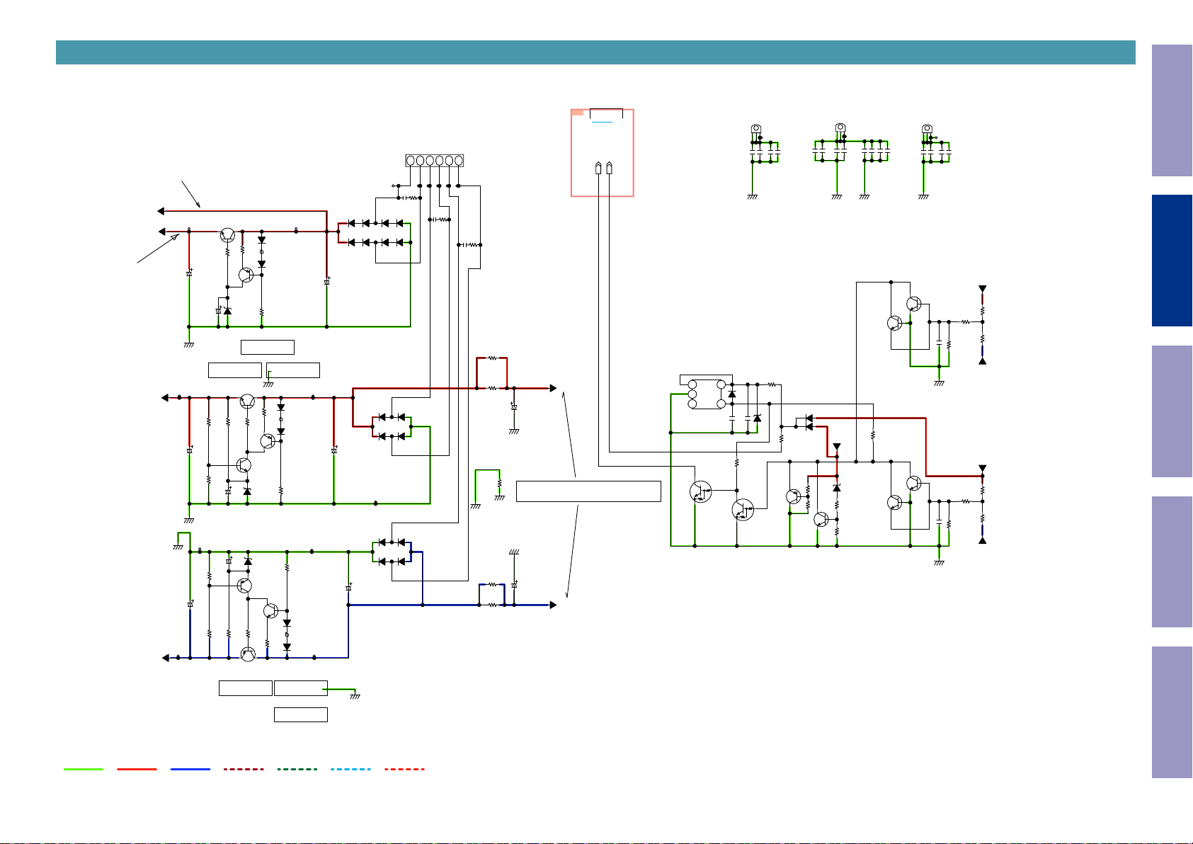
SCH14_AUDIO(3/4)
approx. 15V
+10V
+8V
8.5V
C6003
470/25
AGND
+15V
R6001
C6004
470/25
to AUDIO
-15V
AGND
AGND
C6005
R6002
R6003
470/25
R6004
Q6001
2SC4883(O/Y)
68
R6005
C6008
100/25
Z6204
SCREW
R6006
3.3K
4.7K
3.9K
C6009
220/25
C6010
220/25
3.9K
4.7K
R6007
3.3K
2SB1259
R6008
180
UDZS9.1B
D6001
TR_SHIELD
44541021300AS
Q6004
2SD2081
68
R6009
D6002
UDZS6.2B
D6003
UDZS6.2B
68
R6010
Q6005
Z6205
SCREW
Q6006
Z6104
Q6002
23
D6004
1
1SS302
KTA1266GR
6.8K
R6011
AGND
Z6004
HEAT-SINK
POWER FOR AUDIO(I/V,LPF,BUFFER)
AGND
23
1
D6005
R6012
100
1SS302
Q6007
KTA1266GR
KTC3198GR
10K
R6014
AGND
AGND
10K
R6015
Q6003
KTA1266GR
Q6008
KTC3198GR
23
1
D6006
1SS302
R6013
100
POWER FOR D/A CONVERTOR
Z6005
HEAT-SINK
00M009D267010
Z6105
TR_SHIELD
44541021300AS
11V02N11V03N11V1411V15N8V6P8V
1
R6034
OPEN
D6007
D6024
11EQS10
11EQS10
C6011
1000/35
00M009D267010
使用不可
AGND
D6025
C6012
C6013
4700/35
11EQS10
D6008
11EQS10
D6009
11EQS10
D6010
11EQS10
4700/35
D6011
11EQS10
11EQS10
使用不可
AGND
D6013
11EQS10
D6014
11EQS10
D6012
D6026
11EQS10
D6027
11EQS10
D6015
11EQS10
D6016
11EQS10
D6017
11EQS10
D6018
11EQS10
AUDIO POWER
OPEN
R6036
All Ref.No. has been described in the parts list are four digits.
But there are less than four digits of printed Ref.No. on the PCB, and they have become four digits after the header by adding "0" in the parts list.
to DISCRETE DAC SHEET
GND-TERMINAL
IN
5
OUT
4
0.1
C6018
B7004
C6022
AGND
KDS160
D6023
0.1
C6019
R6033
Q6009
KRC102S
AGND
0.1
3.3K
1000P
C6024
R6025
680
D6022
C6042
0.01
C6041
UDZS18B
Q6010
KTA1504S
100P
D6019
KDS160
KDS160
D6020
R6018
3.3K
R6019
100P
C6045
18K
R6020
Q6011
KTC3875S
0.01
C6046
D6021
4.7K
0.1
C6025
AGND
+8V
UDZS8.2B
B7006
GND-TERMINAL
0.1
C6028
1000P
C6027
AGND
R6021
10K
10K
R6022
1000P
C6029
Q6015
R6032
Q6012
C6048
0.01
C6047
KTC3875S
3.3K
KTC3875S
100P
0.1
C6030
GND
KTC3875S
Q6016
KTC3875S
Q6013
B7005
GND-TERMINAL
0.01
1000P
C6031
C6043
1u
C6062
AGND
1u
C6026
AGND
100P
C6044
R6038
4.7K
4.7K
R6037
R6027
1K
OPEN
R6026
+18V
-18V
+15V
-15V
10K
R6039
10K
R6040
10K
R6028
10K
R6029
N601
6P-VH
AGND
R6035
OPEN
R6030
82(1W)
R6016
82(1W)
2200/35
AGND
Actual voltage of "+18V" and "-18V"
R6024
OPEN
are approx. +21V and -21V.
AGND
AGND
R6031
82(1W)
AGND AGND
C6015
R6017
82(1W)
C6014
2200/35
+18V
-18V
7C
TO C7
VOLT_PROT_1
VOLT_PROT_2
BIDIRECT
BIDIRECT
U6001
NJM2831F33
1
CT
GND
2
NC
3
Q6014
KRC102S
Caution in
servicing
Electrical Mechanical Repair Information Updating
GND LINE
POWER+ LINE
POWER- LINE
ANALOG AUDIO R ANALOG AUDIO L
DIGITAL AUDIO
STBY POWER
22
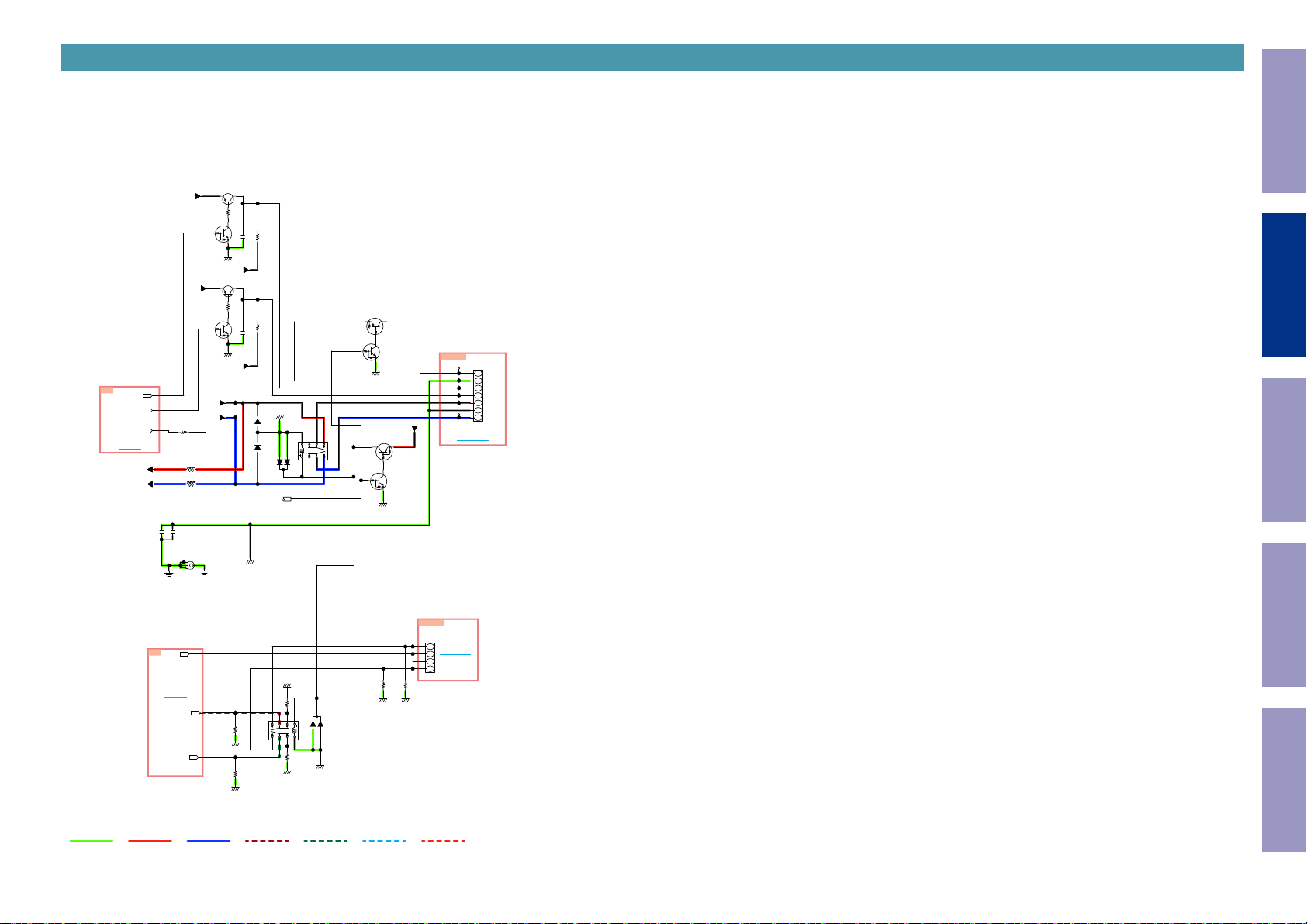
SCH15_AUDIO(4/4)
Audio PWB
+18V.
KRC102S
Q6533
+18V.
KRC102S
Q6535
C8
BIDIRECT
HPGAIN_HI
HPGAIN_MID
M_RELAY
TO 8C
+18V
-18V
BIDIRECT
BIDIRECT
R6023
BLM21PG221
0
L6501
L6502
BLM21PG221
+18V.
-18V.
2SA1312(B)
Q6534
10K
R6574
AGND
-18V.
2SA1312(B)
Q6536
10K
R6575
AGND
-18V.
47P
C6525
47P
C6526
D6031
1SR154
D6032
1SR154
R6564
100K
R6565
100K
D6030
AGND..
2
1SS301
H.P_ON/OFF
All Ref.No. has been described in the parts list are four digits.
But there are less than four digits of printed Ref.No. on the PCB, and they have become four digits after the header by adding "0" in the parts list.
Caution in
servicing
Electrical Mechanical Repair Information Updating
Q6540
KRA102S
Q6539
KRC102S
AGND
Q6538
S6001
KRA102S
G6K-2P-Y
Q6537
KRC102S
AGND..
817 6 5
3
2 3 4
1
OUTPUT
R_12V
N703
N703
7P-PH
TO N713
1
2
3
4
5
+18V
6
AGND
7
-18V
GND LINE
C6020
1000P
6C
POWER+ LINE
C6023
GND-TERMINAL
FG10
AGND
TO C6
R_BUFOUT
L_BUFOUT
0.1
B6003
EARTH
POWER- LINE
AGND..
S6002
G6K-2P-Y
R6578
47K
AGND
AGND
R7867
4.7K
R6579
47K
ANALOG AUDIO R ANALOG AUDIO L
AGND
234
AGND
R7868
4.7K
81765
3
AGND..
N402
N402
4P-PH
1
TO N412
2
3
4
R6576
R6577
47K
47K
DIGITAL AUDIO
AGNDAGND
STBY POWER
1
D6028
1SS301
2
23
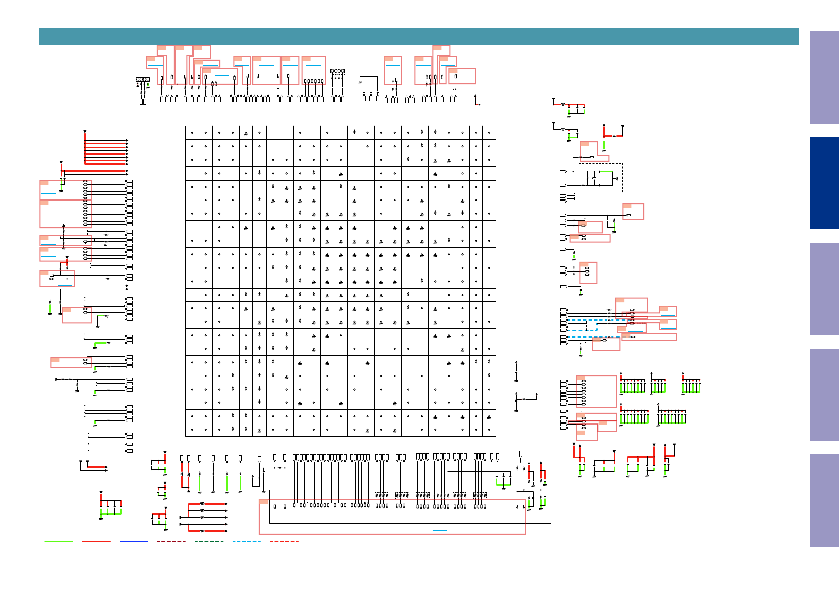
SCH16_MECHA(1/4)
3.3V2URXD3UTXD4GND
N0481
4P-PH
1
3.3V
R2021
0
3.3V
3.3V
3.3V
3.3V
3.3V
3.3V
USB_DP_P0
USB_DM_P0
0.1
0.1
C2003
0
0
0
0
0
0
0
SD_DATA3
5.1K
5.1K
USB_DP_P2
USB_DM_P2
5.1K
24K
3.3V
1.2V
C2004
0.1
0.1
C2005
C2006
POWER- LINE
3.3V_STBY
AC2
AC1
AB3
AB1
AB2
AC3
AA3
AA2
Y3
Y2
Y1
W3
W2
V4
N20
P20
M21
R21
L23
M22
L21
M20
L22
J21
J22
T2
T1
V3
T3
U2
U3
T4
V2
V1
K21
K22
K20
U22
T21
T22
U23
E22
E21
F22
E23
G23
G22
H22
H21
J23
C23
C22
C21
D22
3.3V
3.3V
3.3V
3.3V_STBY
FSRC_WR
FSRC_RD
NFALE
NFCEN
NFCLE
NFRBN
NFREN
NFWEN
NFD0
NFD1
NFD2
NFD3
NFD4
NFD5
NFD6
NFD7
GPIO0
GPIO1
GPIO2
GPIO3
GPIO4
GPIO5
GPIO6
GPIO7
GPIO8
LED0
LED1
SCL
SDA
SD_CMD
SD_DET
SD_CLK
SD_DATA0
SD_DATA1
SD_DATA2
SD_DATA3
USB_DP_P0
USB_DM_P0
USB_VRT_P0
USB_VBUS_P1
USB_DM_P1
USB_DP_P1
USB_VRT_P1
USB_VBUS_P2
USB_DP_P2
USB_DM_P2
USB_VRT_P2
TXVN_0
TXVP_0
TXVN_1
TXVP_1
REXT
GPIO32
GPIO31
GPIO30
GPIO33
E5
TO 5E
E6
TO 6E
R2004
E7
TO 7E
E8
TO 8E
R2002
4.7K
MFI_SCL
E9
BIDIRECT
BIDIRECT
MFI_SDA
4.7K
R2001
DGND
F1
TO 1F
5V_STBY
GND LINE
3.3V_STBY
0.1
C2001
DGND
10K
R2005
10K
DGND
TO 9E
0
R2003
DGND
R2006
1M
0.1
C2002
3.3V
F0
3.3V
R2007
R2008
1M
4.7K
TO 0F
USB_DM_P1
USB_DP_P1
NFALE
NFCEN
NFCLE
NFRBN
NFREN
NFWEN
NFD0
NFD1
NFD2
NFD3
NFD4
NFD5
NFD6
NFD7
GPIO3.
GPIO5
GPIO6
GPIO7
GPIO8
SD_DATA0
SD_DATA1
DGND
R2009
1M
1.2V
BIDIRECT
BIDIRECT
BIDIRECT
BIDIRECT
BIDIRECT
BIDIRECT
BIDIRECT
BIDIRECT
BIDIRECT
BIDIRECT
BIDIRECT
BIDIRECT
BIDIRECT
BIDIRECT
STR_PW_CTL
R2011
R2012
R2013
BIDIRECT
R2010
BIDIRECT
BIDIRECT
BIDIRECT
BIDIRECT
LED0
LED1
R2015
R2016
SD_CMD
SD_DET
SD_CLK
BIDIRECT
BIDIRECT
R2014
DGND
R2017
DGND
BIDIRECT
BIDIRECT
R2018
DGND
R2019
DGND
TXVN_0
TXVP_0
TXVN_1
TXVP_1
R2020
DGND
3.3V
3.3V
DGND
POWER+ LINE
D1
D2
TO 1D
TO 2DD3TO 3D
C9
TO 9C
OP-
LIMIT
TROPEN
INPUT
INPUT
INPUT
0
0
0
DGND
R2022
R2024
R2025
R2023
0
K6
J1
P1
K7
R3
R2
FEGIO9
FEGIO7K5FEGIO5
FEGIO4
FEGIO6
FEGIO11
FEGIO10
A1
A
B1
B
C1
C
D
E1
E
F
G1
G
H
J1
J
K1
K
L
M1
M
FETRAYIN
FETRAYIN_M2FEGIO0
N
P1
P
R
T1
T
U
V1
V
SD_DATA3 SD_DATA2
SD_DATA3V2SD_DATA2V3SD_CMDV4NFD7V5DVCC12_KV6DVCC12_KV7DDRVCCIOV9DGND12_K
W
Y1
Y
AA
AB1
AB
AC1
AC
3.3V_STBY
M19
AVDD33_PLLGP
AVDD33_LDO
C2012
C2009
C2007
1000P
0.1
0.1
BLM21PG221
DGND
3.3V
L2001
C2013
C2010
0.1
1000P
3.3V_STBY
DGND
3.3V
C2011
0.1
C2014
C2008
1000P
0.1
3.3V_STBY
3.3V
DGND
ANALOG AUDIO R ANALOG AUDIO L
D4
TO 4D
D5
OPO
MUTE1
TRCLOSE
INPUT
INPUT
INPUT
0
0
R2029
R20270R2026
N4
K4
FEGIO3
FEGIO1
2 3 4 5 6 7 8
1
A2
INA
VDAC0 FVREF
VDAC0A3FVREFA4FPDOCDA5AVSS33_PLLGPA6NS_XTALI
INA
INC INB
INCB2INBB3VWDC3OB4FPDODVDB5AVDD33_PLLGPB6NS_XTALO
INH ING IND
INHC2INGC3INDC4VWDC2O
D2
INE INF
INED3INF
TRINA TRINB
TRINAE2TRINBE3V14E4AUX1
F2
TRIND TRINC
TRINDF3TRINCF4MPXOUT3F6AVDD12F7DGND12_KF8DGND12_KF9DGND12_K
RFIN RFIP
RFING2RFIPG3TLO
FEGAINSW1 FEGAINSW2
FEGIO5
FEGIO5J2FEGAINSW1J3FEGAINSW2
FECFREQ FEOSCEN
FECFREQK2FEOSCENK3FECMODK4FEGIO1K5FEGIO7K6FEGIO9K7FEGIO6K8DVCC33_IOK9DVCC12_K
L2
FEEJECT_
FEEJECT_L3FETRAYOUT_L4FEFMO4L5FEFMO3L6FEDMOL7DVCC33_IOL8DVCC33_IOL9DVCC12_K
FEGIO0
N2
FEFMO
FEFMON3FEFMO2N4FEGIO3N5FSRC_WRN6FSRC_RDN8DGND12_KN9DVCC12_K
FEGIO4
FEGAINSW3 FETRAYPWM
FEGIO4P2FEGAINSW3P3FETRAYPWMP4FEFGP5DGND12_KP7DGND12_KP9DVCC12_K
R2
FEGIO10 FEGIO11
FEGIO10R3FEGIO11
SDA SCL
SDAT2SCLT3SD_DETT4SD_DATA1T5GPIO25T6DVCC12_KT7DVCC12_KT8DVCC12_K
U2
SD_CLK
SD_CLKU3SD_DATA0U5DVCC12_KU6DVCC12_KU7DVCC12_KU8DDRVCCIO
W2
NFD6 NFD5
NFD6W3NFD5W4DVCC12_KW6DDRVCCIOW7DDRVCCIOW8DGND12_KW9RDQ2
NFD4 NFD3 NFD2
NFD4Y2NFD3Y3NFD2Y4DVCC12_KY5DDRVCCIOY6DDRVCCIOY8RDQ6Y9RDQ0
AA2
NFD1 NFD0
NFD1
AB2
NFRBN NFREN NFCLE
NFRBN
NFREN
AC2
NFCEN NFALE NFWEN
NFCEN
NFALE
U2001
ARTP
B5
U13
R2028
BLM21PG221
120
L2002
L2003
BLM21PG221
L2004
L2005
L2007
BLM21PG221
D6
TO 6DD7TO 7DD8TO 8D
DMO
TO 5D
TRO
FOO
INPUT
INPUT
H3
H4
M2
FOO
FEGIO0
VWDC3O
H3
FOOH4TROH5DGND12_KH7DGND12_KH8DVCC33_IOH9DVCC33_IO
FECMOD FEGIO1 FEGIO7 FEGIO9 FEGIO6
FETRAYOUT_
FEFMO2 FEGIO3
SD_DET
SD_DATA0
SD_CMD
AA3
NFD0
AB3
NFCLE
AC3
NFWEN
ARTN
U14
R2030
47
DGND
BLM21PG221
BLM21PG221
FMO
INPUT
R2032
0
L5
L6
P3
N3
G3
L4
TRO
TLO
FEDMO
FEFMO3
FEFMO2
FEFMO4
FETRAYPWM
FPDOCD
DGND
FPDODVD
AVDD33_PLLGP
VWDC2O
D5
HAVC
HAVCD6AVDD33_1D7AOLRCKD8AOSDATA1D9AOSDATA3
V14
AUX1
MPXOUT3
G5
TLO
MPXOUT2 MPXOUT1
MPXOUT2G6MPXOUT1
FOO TRO
DGND DGND
FEFMO4 FEFMO3
FSRC_WR FSRC_RD
FEFG
DGND DGND
SD_DATA1
1.2V 1.2V 1.2V 1.5V
1.2V 1.2V 1.5V
NFD7
1.2V 1.5V 1.5V
1.2V 1.5V 1.5V
AB4
AB5
1.2V 1.5V
DVCC12_K
DDRVCCIO
AC4
AC5
1.2V 1.5V
DVCC12_K
DDRVCCIO
MEM_TP
MEM_TN
U16
U17
R2033
R2031
47
47
DGND
DGNDDGND
AVDD33_USB_P0
AVDD33_LD
AVDD33_COM
3.3V
(AVDD33_USB_P1)
to_U2001_V23
AVDD33_USB_P2
DIGITAL AUDIO
RFO
INPUT
INPUT
INPUT
FEGAINSW1
R2034
0
P2
N2
K1
K2
K3
J2
J3
FEFMO
FECMOD
FECFREQ
FEOSCEN
FEGAINSW3
FEGAINSW1
FEGAINSW2
NS_XTALI
NS_XTALO
C7
AOSDATA0 AOSDATA2
AOSDATA0C8AOSDATA2C9SPDIF
A3.3V
AOLRCK
E7
A3.3V
AVDD33_3E8DGND12_KE9DGND12_K
AVDD12
DGND DGND DGND DGND
3.3V 3.3V 1.2V
FEDMO
R6
1.2V 1.2V 1.2V
DGND
DGND12_KR7DVCC12_KR8DVCC12_KR9DVCC12_K
1.2V 1.2V 1.2V
AA6
1.5V
DDRVCCIO
AB6
AB7
DDRVCCIO_CK
RDQ11 RDQ15 RDQM1 RDQS0
DDRVCCIO_Ck
RDQ11
AC6
AC7
RDQ9
DGND
DGND12_K
RDQ9
RCLK0
DDRVCCIO_CK
AB15
AB6
R2036
C2015
1.5V
0
1000P
R2035
DGND
F2
OUTPUT
RCLK0
STBY POWER
FPDOCD
INPUT
C2016
0.1
G1
G2
A4
B4
RFIN
RFIP
FPDOCD
FPDODVD
A9
SPDIF_IN1
SPDIF_IN1
B9
SPDIF_IN0
SPDIF_IN0
SPDIF
AOSDATA1 AOSDATA3
DGND DGND DGND DGND
G9
3.3V
DVCC33_IO
3.3V 3.3V
J8
3.3V 1.2V 1.2V
DVCC33_IOJ9DVCC12_K
3.3V 1.2V 1.2V
M8
3.3V 1.2V
DVCC33_IOM9DVCC12_K
1.2V 1.2V
DGND
1.2V
DGND DGND DGND DGND DGND
RDQ2 RDQ3 RDQ7 RODT RCS_ RBA2 RA13
DGND
RDQ6 RDQ0 RDQ1 RDQ5 RCKE
AA8
AA9
RDQ4
DGND
RDQ4
DGND12_K
AB8
AB9
RDQ15
RDQM1
AC8
RDQ13
RDQ13
RDQ0
RDQ1
RCLK0_
Y9
AC15
100
100
BIDIRECT
OUTPUT
RDQ0
RCLK0_
All Ref.No. has been described in the parts list are four digits.
But there are less than four digits of printed Ref.No. on the PCB, and they have become four digits after the header by adding "0" in the parts list.
D9
TO 9D
INC
INE
INF
IND
INPUT
INPUT
INPUT
INPUT
D2
D3
C1
C2
INE
INF
INDC3INH
ING
10 11 12 13 14 15 16
9
B10
AL0
AL0
C10
AR0
AR0
D10
3.3V
AVDD33_DAC
E10
AVSS33_DAC
F10
DGND12_K
G10
DGND DGND DGND DGND DGND
DGND12_K
H10
DGND DGND DGND DGND DGND DGND DGND
DGND12_K
J10
DVCC12_K
K10
DVCC12_K
L10
DGND DGND DGND DGND DGND DGND DGND
DGND12_K
M10
DGND DGND DGND DGND DGND DGND DGND
DGND12_K
N10
DVCC12_K
P10
DGND DGND DGND DGND DGND DGND
DGND12_K
R10
DGND DGND DGND DGND DGND DGND DGND DGND DGND
DGND12_K
T10
DGND DGND
DGND12_K
U10
DGND
DGND12_K
AA10
RDQM0
RDQM0
AB10
RDQS0
AC10
RDQS0_
RDQS0_
RDQ5
RDQ3
RDQ2
RDQ6
RDQ4
W9
Y8
Y13
W11
Y11
AA8
BIDIRECT
BIDIRECT
BIDIRECT
BIDIRECT
RDQ2
RDQ6
RDQ3
RDQ5
N0491
123
4
4P-PH
INA
INB
INPUT
INPUT
0
0
0
C2018
C20200C2019
C2017
F2
E1
F3
E2
B1
A1
B2
INC
INA
INB
TRIND
TRINA
TRINC
TRINB
A11
A13
3.3V
AVDD33_10
B12
RSRV_14
RSRV_15
C12
RSRV_16
RSRV_17
D12
DGND
DGND12_K
E13
E12
3.3V
DGND12_K
AVDD33_11
F13
DGND
DGND12_K
G12
G13
DGND12_K
DGND12_K
H12
H13
DGND12_K
DGND12_K
J12
J13
DGND DGND DGND DGND DGND DGND DGND DGND DGND
DGND12_K
DGND12_K
K12
K13
DGND DGND DGND DGND DGND DGND DGND DGND DGND
DGND12_K
DGND12_K
L12
L13
DGND12_K
DGND12_K
M12
M13
DGND12_K
DGND12_K
N12
N13
DGND DGND DGND DGND DGND
DGND12_K
DGND12_K
P12
P13
DGND12_K
DGND12_K
R12
R13
DGND12_K
DGND12_K
T12
DDRVREF
DDRVREF
U13
ARTP ARTN
ARTP
W13
RDQ3
RDQ7
Y13
RDQ1
RDQ5
AA12
DGND DGND
DGND12_K
AB12
AB13
RDQS1_
RDQ12
RDQ8
RDQS1_
RDQ12
RDQ8
AC13
RDQS1 RDQ14
RDQS1
RDQ14
RDQM0
RDQ12
RDQ14
RDQ9
BIDIRECT
RDQ9
RDQM1
RDQ13
RDQ11
RDQ10
RDQ15
AC7
AB9
AC8
AB7
AB8
AA10
AB12
AC13
AB14
BIDIRECT
BIDIRECT
BIDIRECT
BIDIRECT
BIDIRECT
BIDIRECT
RDQ15
RDQ10
RDQM1
RDQ14
RDQ12
RDQM0
RDQ7
W13
BIDIRECT
RDQ7
VMID_PWMDAC
VMID_PWMDAC
B11
C11
G11
DGND12_K
H11
DGND12_K
J11
DGND12_K
K11
DGND12_K
L11
DGND12_K
M11
DGND12_K
N11
DGND12_K
P11
DGND12_K
R11
DGND12_K
T11
DGND12_K
V11
DGND12_K
W11
Y11
AB11
AC11
RDQ8
AB13
BIDIRECT
RDQ8
E0
TO 0E
DGND
R2038
4.7u
4.7u
OPEN
C2023
C2022
C2021
0
E3
D5
A3
L2
V14
HAVC
FVREF
FEEJECT_
A14
A15
A16
CH2_P CH1_P CH0_P CLK_P
RSRV_18
RSRV_19
B14
B15
B16
CH2_M CH1_M CH0_M CLK_M
RSRV_22
RSRV_23
C15
HDMISD
GPIO35
D15
D16
HDMISCK
GPIO36
E15
RSRV_15
RSRV_12
F15
F16
CEC
GPIO37
G15
RSRV_13
H16
J14
J15
J16
DGND12_K
DGND12_K
K14
K15
K16
DGND12_K
DGND12_K
L14
L15
L16
DGND12_K
DGND12_K
M14
M15
M16
DGND12_K
DGND12_K
N14
N15
DGND12_K
DGND12_K
P14
P15
DGND12_K
DGND12_K
R14
R15
R16
DGND12_K
DGND12_K
U14
U16
ARTN
V14
DGND12_K
W15
W16
RODT
Y15
RCKE
AA16
AB14
AB15
AB16
RDQ10 RCLK0
RDQ10
RCLK0
AC14
AC15
AC16
RCLK0_
DGND
DGND12_K
RCLK0_
RA10
RA4
RDQS1
RDQS1_
RDQS0_
RDQS0
RA1
RA6
AB16
AB17
AC11
AB11
AC10
AB10
AA17
AC18
1 2
3 4
5 6
7 8
R2037
BIDIRECT
BIDIRECT
BIDIRECT
BIDIRECT
OUTPUT
OUTPUT
OUTPUT
OUTPUT
RDQS1
RDQS1_
RDQS0_
RDQS0
1_RA1
1_RA6
1_RA4
1_RA10
FETRAYIN_
FETRAYOUT_
INPUT
INPUT
R2039
M1
L3
FETRAYIN
FETRAYOUT_
RSRV_20
RSRV_24
HTPLG
GPIO38
GPIO23
GPIO23
DGND12_K
DGND12_K
DGND12_K
DGND12_K
DGND12_K
DVCC33_IO_STB
DVCC33_IO_STB
DGND12_K
MEM_TP MEM_TN
MEM_TP
RCS_
DGND12_K
RA10
RA10
DGND
DGND12_K
RA8
AB18
75x4
R2040
5 6
7 8
OUTPUT
OUTPUT
1_RA8
0
A17
B17
C17
E17
F17
H17
DGND12_K
J17
DGND12_K
K17
DGND12_K
N17
P17
R17
DGND12_K
U17
Y17
AA17
AB17
RA11
AC19
1_RA11
TO DDR3
E1
TO 1E
B3
F4
G5
G6
VWDC3O
MPXOUT3
MPXOUT2
MPXOUT1
A18
1.2V
RSRV_21
AVDD12_0
B18
1.2V 3.3V
RSRV_25
AVDD12_1
C18
1.2V
AMUTE
AVDD12_2
AMUTE
E18
GPIO22 GPIO21
GPIO24
GPIO24
GPIO22
F18
GPIO20
DGND DGND
GPIO20
DGND12_K
G18
DGND12_K
H18
DGND12_K
J18
DGND12_K
K18
DGND12_K
M18
AVDD12_LDO
AVDD12_LDO
3.3V_STBY
P18
3.3V_STBY
RESET_
RESET_
MEM_TN
W18
RBA2
RCSX_
RCSX_
RA1
RA1
AB18
RA4 RA8
RA4
RA8
AC18
RA6
RA6
RRAS_
RBA1
RCAS_
RA12
AC21
AA20
AC22
AB20
75x4
R2042
1 2
3 4
3 4
5 6
7 8
OUTPUT
OUTPUT
OUTPUT
OUTPUT
1_RBA1
1_RA12
1_RRAS_
1_RCAS_
E2
TO 2E
E3
TO 3E
E4
LDO1
LD02
GPIO23
GPIO24
INPUT
INPUT
INPUT
INPUT
0
0
R2041
R2043
F16
E17
A2
C4
E4
AUX1
VDAC0
VWDC2O
GPIO24
GPIO23
20191817 21 2322
A19
A20
3.3V
AVDD33_12
RSRV_01
B19
B20
AVDD33_0
RSRV_07
C19
C20
DGND DGND
DGND12_K
DGND12_K
D19
DGND
DGND12_K
E20
E19
AVDD33_USB_P2
AVDD33_USB_P2
GPIO21
G19
G20
AVDD33_LD
DGND
AVDD33_LD
DGND12_K
J19
J20
AVDD33_USB_P0
DGND12_K
AVDD33_USB_P0
K19
K20
USB_VRT_P0
DGND12_K
USB_VRT_P0
M19
M20
GPIO7 GPIO2 GPIO5
AVDD33_LDO
AVDD33_LDO
GPIO7
N20
GPIO0
GPIO0
P19
P20
GPIO1
DGND
DGND12_K
GPIO1
R19
DGND12_K
T19
T20
DGND DGND
DGND12_K
DGND12_K
V20
DGND12_K
W20
RA13
Y19
RA0 RA9 RA3
RA0
AA19
AA20
RA14 RBA1 RWE_
RA14
RBA1
AB19
AB20
RA12
DGND
DGND12_K
RA12
AC19
RA11
RA11
RBA2
RWE_
RCS_
RCKE
RA0
RA13
RODT
W18
W16
Y15
Y19
W15
AA21
75x4
0
R2049
1 2
7 8
R20440R20450R20460R20470R2048
OUTPUT
OUTPUT
OUTPUT
OUTPUT
OUTPUT
OUTPUT
OUTPUT
1_RA0
1_RBA2
1_RCS_
1_RODT
1_RA13
1_RCKE
1_RWE_
TO 2F
TO 4E
FEFG
INPUT
AVDD12
P4
FEFG
A21
A22
RSRV_02
RSRV_03
B21
B22
RSRV_08
RSRV_09
C21
C22
GPIO30 GPIO31 GPIO32
GPIO30
GPIO31
D21
D22
GPIO33
RSRV_11
GPIO33
E21
E22
USB_DP_P2
USB_VBUS_P2
USB_DP_P2
USB_VBUS_P2
F21
F22
USB_DM_P2
DGND12_K
USB_DM_P2
G21
G22
AVDD33_COM
TXVP_0 TXVN_0
AVDD33_COM
TXVP_0
H21
H22
TXVP_1 TXVN_1
TXVP_1
TXVN_1
J21
J22
LED0 LED1 REXT
LED0
LED1
K21
K22
USB_DP_P0 USB_DM_P0
USB_DP_P0
USB_DM_P0
L21
L22
GPIO6 GPIO8 GPIO4
GPIO6
GPIO8
M21
M22
GPIO2
GPIO5
N21
N22
OPWRSB
VDATA
OPWRSB
VDATA
P21IRP22
IR
VCLK
VCLK
R21
R22
GPIO3 UATXD UARXD
GPIO3
UATXD
T21
T22
USB_DP_P1USB_DM_P1
USB_DM_P1
USB_DP_P1
U21
U22
USB_VBUS_P1
DGND
AVSS33_DDR
USB_VBUS_P1
V21
V22
3.3V 3.3V
DGND12_K
AVDD33_DDR
Y21
Y22
RA9
RA3
AA21
AA22
RA2 RA5
RWE_
RA2
AB21
AB22
RA7
DGND
DGND12_K
RA7
AC21
AC22
RRAS_ RCAS_
RRAS_
RCAS_
RRESET
RA2
RA7
RA9
Y21
W20
AC23
AA22
AB22
75x4
R2050
1 2
3 4
5 6
5 6
7 8
OUTPUT
OUTPUT
OUTPUT
OUTPUT
OUTPUT
1_RA2
1_RA7
1_RA9
1_RRESET
AVDD12
A23
B23
C23
E23
USB_VRT_P2
USB_VRT_P2
G23
TXVN_0
J23
L23
GPIO4
N23
R23
UARXD
U23
USB_VRT_P1
USB_VRT_P1
V23
AVDD33_USB_P1
W23
AVDD12_DDR
Y23
AA23
AB23
DGND12_K
AC23
RRESET
RRESET
RA3
RBA0
RA5
Y22
AA23
1 2
3 4
OUTPUT
OUTPUT
1_RA5
1_RA3
1_RBA0
RSRV_04
RSRV_10
GPIO32
REXT
VSTB
VSTB
AVDD12_DDR
RBA0
RBA0
RA5
DGND
Y23
75x4
Caution in
servicing
3.3V_STBY
L2008
BLM21PG221
0.1
0.1
4.7u
C2035
C2033
C2039
DGND
3.3V_STBY
L2009
BLM21PG221
NS_XTALI
NS_XTALO
GPIO20
GPIO21
GPIO22
RESET_
OPWRSB
AMUTE
UARXD
UATXD
IR
VSTB
VCLK
VDATA
VMID_PWMDAC
AL0
AR0
AOLRCK
AOSDATA0
AOSDATA1
AOSDATA2
AOSDATA3
SPDIF
SPDIF_IN0
SPDIF_IN1
3.3V
AVDD12_LDO
0.1
4.7u
C2036
C2034
DGND
F3
TO 3F
R2061
0
INPUT
A6
OPEN
R2064
B6
R2062
OPEN
F17
E19
E18
P18
R2058
0
N21
R2059
F5
INPUT
BE_MUTE_REQ
C18
0
TO 5F
INPUT
UARXD
R23
F6
INPUT
UATXD
R22
P21
R2060
10K
DGND
F7
BIDIRECT
N23
VSTB
BIDIRECT
P22
VCLK
BIDIRECT
N22
VDATA
TO 7F
A11
0.1
C2038
DGND
B10
C10
D7
C7
D8
C8
D9
C9
B9
A9
R2063
10K
DGND
1000P
C2027
DGND
AVDD12_DDR
1.2V
R2052
0
0.1
C2028
DGND
DDRVREF
RCSX_
RA14
T12
Y17
AA19
C2024
OPEN
OPEN
C2025
DGND
C2026
OPEN
0
R2051
VREFDQ
OPEN
R2053
VREFCA
1.5V
1.5V
1K
1K
0.1
C2031
C2029
CK0.1
CK0.1
DGND
DGND
R2056
R2054
1K
1K
0.1
C2032
C2030
CK0.1
CK0.1
R2057
R2055
DGND
DGND
G4
INPUT
CH0_M
CH0_P
CH1_M
CH1_P
CH2_M
CH2_P
CLK_M
CLK_P
RSRV_15
HTPLG
CEC
HDMISD
HDMISCK
0.1
CH0_M
B16
INPUT
CH0_P
A16
INPUT
CH1_M
B15
INPUT
CH1_P
A15
INPUT
CH2_M
B14
INPUT
CH2_P
A14
INPUT
CLK_M
B17
INPUT
CLK_P
A17
TPI1
E15
G5
INPUT
HTPLG
D16
INPUT
CEC
F15
INPUT
HDMISD
C15
INPUT
HDMISCK
D15
G7
TO 7G
3.3V
3.3V
A19
1000P
0.1
C2040
C2037
DGND
0.1
G3
0.1
C2041
DGND
C2044
8501_27MHz
C2042
OPEN
OPEN
C2043
OPEN
C2046
0.1
TO 6F
R2065
R2066
R2067
R2068
R2069
R2070
INPUT
TO 3G
TO 4G
TO 5G
G6
TO 6G
OPEN
DGND
OPEN
X2001
OPEN
1.2V
M18
R2071
OPEN
NOT USE
DGND
OPEN
F4
TO 4F
INPUT
RESET_
R2072
10K
DGND
F8
TO 8F
INPUT
0.1
C2045
SPDIF_IN0
47
INPUT
47
INPUT
47
INPUT
47
INPUT
47
G1
TO 1G
INPUT
47
G2
1.5V
4.7u
0.1
1000P
10/10
C2050
C2052
C2055
C2048
DGND
1.5V
0.1
0.1
0.1
0.1
C2049
C2051
C2053
C2056
DGND
3.3V
0.1
0.1
C2054
C2047
DGND
AO_BCK
8501_AUDIO_MCK
AO_LRCK
AO_SDATA0/DSD_LCH
DSD_RCH
SPDIF_OUT
0.1
0.1
0.1
C2057
C2059
C2062
0.1
0.1
0.1
C2058
C2060
C2063
0.1
C2061
0.1
C2064
0.1
C2065
DGND
0.1
C2066
1.5V
DGND
10/10
C2067
TO 2G
0.1
10/10
1000P
C2068
C2070
C2071
1.2V
10/10
C2072
DGND
1.2V
1000P
C2069
F9
TO 9F
G0
TO 0G
0.1
0.1
C2075
C2073
4.7u
10/10
C2074
C2076
3.3V
D10
1000P
C2077
E10
DGND
1000P
C2078
0.1
C2080
3.3V
0.1
C2079
0.1
C2081
0.1
C2082
1.2V
0.1
0.1
4.7u
0.1
10/10
10/10
C2089
C2090
C2086
C2087
C2088
C2084
DGND
0.1
0.1
C2083
C2085
Electrical Mechanical Repair Information Updating
24
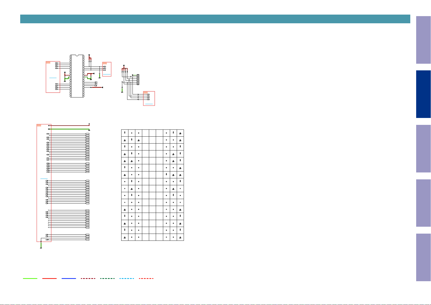
SCH17_MECHA(2/4)
MX30LF2G28AB-TI
(VSS)
48
N.C
47
N.C
46
N.C
6E
NFD7
NFD6
NFD5
NFD4
TO E6
NFD3
NFD2
NFD1
NFD0
45
I/O7
INPUT
44
I/O6
INPUT
43
I/O5
INPUT
42
I/O4
INPUT
41
N.C
40
3.3V
(VCC)
39
N.C
38
Vcc
37
Vss
36
0.1
N.C
35
C2091
(VCC)
34
N.C
33
DGND
I/O3
INPUT
32
I/O2
INPUT
31
I/O1
INPUT
30
I/O0
INPUT
29
N.C
28
N.C
27
N.C
26
(VSS)
25
U2002
All Ref.No. has been described in the parts list are four digits.
But there are less than four digits of printed Ref.No. on the PCB, and they have become four digits after the header by adding "0" in the parts list.
Caution in
servicing
3.3V
1
N.C
2
N.C
3
N.C
4
N.C
4.7K
OPEN
5
N.C
6
N.C
7
R/B#
8
RE#
9
CE#
N.C
10
N.C
11
Vcc
12
Vss
13
N.C
14
N.C
15
CLE
16
ALE
17
WE#
18
R2075
WP#
19
N.C
20
N.C
21
N.C
22
N.C
23
N.C
24
R2074
C2092
5E
R2076
INPUT
NFRBN
INPUT
NFREN
INPUT
NFCEN
TO E5
3.3V
1000P
C2093
0.1
DGND
DGND
INPUT
NFCLE
INPUT
NFALE
INPUT
NFWEN
10K
3.3V
3.3V
10K
10K
10K
10K
N0651
6P-PH
1
R2080
R2077
R2079
R2081
DGND
2
3
4
5
R2082
R2083
R2084
R2085
6
8E
0
OUTPUT
GPIO5
0
OUTPUT
GPIO6
0
OUTPUT
GPIO7
0
OUTPUT
GPIO8
TO E8
10K
R2078
DGND
Electrical Mechanical Repair Information Updating
2F
TO F2
1_RA0
1_RA2
1_RA4
1_RA5
1_RA6
1_RA7
1_RA9
1_RA11
1_RA12
1_RA13
1_RBA1
1_RBA2
RCLK0
RCLK0_
VREFDQ
VREFCA
1_RRESET
240
R2073
DGND
-
1.5V
DGND
INPUT
RDQ0
INPUT
RDQ2
INPUT
RDQ3
INPUT
RDQ5
INPUT
RDQ6
INPUT
RDQ7
INPUT
RDQ8
INPUT
RDQ9
INPUT
RDQ10
INPUT
RDQ12
INPUT
RDQ14
INPUT
RDQ15
INPUT
RDQS1
INPUT
RDQS1_
INPUT
RDQS0
INPUT
RDQS0_
INPUT
RDQM1
INPUT
RDQM0
INPUT
INPUT
1_RA1
INPUT
INPUT
INPUT
INPUT
INPUT
INPUT
1_RA8
INPUT
INPUT
INPUT
INPUT
INPUT
INPUT
INPUT
INPUT
INPUT
INPUT
INPUT
1.5V
DGND
RDQ0
E3
RDQ1
F7
RDQ2
F2
RDQ3
F8
RDQ4
H3
RDQ5
H8
RDQ6
G2
RDQ7
H7
RDQ8
D7
RDQ9
C3
RDQ10
C8
RDQ11
C2
RDQ12
A7
RDQ13
A2
RDQ14
B8
RDQ15
A3
RDQS1
C7
RDQS1_
B7
RDQS0
F3
RDQS0_
G3
RDQM1
D3
RDQM0
E7
1_RA0
N3
1_RA1
P7
1_RA2
P3
1_RA3
N2
1_RA4
P8
1_RA5
P2
1_RA6
R8
1_RA7
R2
1_RA8
T8
1_RA9
R3
1_RA10
L7
1_RA11
R7
1_RA12
N7
1_RA13
T3
1_RBA0
M2
1_RBA1
N8
1_RBA2
M3
RCLK0
J7
RCLK0_
K7
1_RCS_
L2
1_RCAS_
K3
1_RODT
K1
1_RRAS_
J3
1_RWE_
L3
1_RCKE
K9
VREFDQ
H1
M8
VREFCA
E1_ZQ
L8
1_RRESET
T2
U2003
K4B2G1646Q-BCMA
1A2 3 4 5 6 7 8 9
A1 A2 A3
1.5V
RDQ15
RDQ13
1.5V
B1 B2 B3 B7 B8 B9
B
DGND
DGND
1.5V
C1 C2 C3 C7 C8 C9
C
D1 D2 D3 D7 D8 D9
D
E1 E2 E3 E7 E8 E9
E
F1 F2 F3 F7 F8 F9
F
G1 G2 G3 G7 G8 G9
G
H1 H2 H3 H7 H8 H9
H
J1 J2 J3 J7 J8 J9
J
K1
K
L1
L
M1
M
N1 N2 N3 N7 N8
N
P1
P
R1 R2 R3 R7 R8
R
T1 T2 T3 T7 T8 T9
RDQ9
RDQ11
1.5V
RDQM1
DGND
RDQ0
DGND
DGND
1.5V
RDQS0
RDQ2
RDQS0_
RDQ6
DGND
1.5V
RDQ4 RDQ7
VREFDQ
1_RRAS_
DGND
1.5V
K2 K3 K7 K8 K9
1_RODT
1_RCAS_
L2 L3 L7 L8
1_RCS_
1_RWE_
M2 M3 M7 M8 M9
1_RBA2
1_RBA0
DGND
1.5V
1_RA0
1_RA3
P2 P3 P7 P8 P9
1_RA2
1_RA5 1_RA1
DGND
1.5V
1_RA7
1_RA9
1_RRESET
1_RA13
DGND
A7 A8 A9
RDQ12
RDQS1_
RDQS1
RDQ8
RDQM0
RDQ1
1.5V
RCLK0
RCLK0_
1_RA10
1_RA12
1_RA11
1.5V
DGND
RDQ14
DGND
1.5V
RDQ10
1.5V
DGND
1.5V
DGND
RDQ3
DGND
DGND
DGND
1.5V
RDQ5
DGND
1.5V
1_RCKE
L9
E1_ZQ
VREFCA
DGND
N9
1.5V
1_RBA1
1_RA4
DGND
R9
1.5V
1_RA6
1_RA8
DGND
GND LINE
POWER+ LINE
POWER- LINE
ANALOG AUDIO R ANALOG AUDIO L
DIGITAL AUDIO
STBY POWER
25
 Loading...