

Page 1
Service
STANDBY
DV2400 /N1S/S1S
Manual
STANDBY
SECTION PAG E
1. TECHNICAL SPECIFICATIONS ............................................................................................... 1
2. CONNECTION FACILITIES ......................................................................................................2
3. INFORMATIONS ....................................................................................................................... 3
4. SERVICE HINTS AND TOOLS.................................................................................................. 4
5. WARNING AND LASER SAFETY INSTRUCTIONS ................................................................. 5
6. TAKING THE DISC OUT OF EMERGENCY............................................................................. 6
7. SERVICE MODE ....................................................................................................................... 6
8. WIRING DIAGRAM ................................................................................................................... 7
9. BLOCK DIAGRAM .................................................................................................................... 9
10. SCHEMATIC DIAGRAM.......................................................................................................... 13
11. PARTS LOCATION.................................................................................................................. 21
12. MICROPROCESSOR AND IC DATA....................................................................................... 27
13. EXPLODED VIEW AND PARTS LIST..................................................................................... 33
14. ELECTRICAL PARTS LIST..................................................................................................... 36
DVD Player
DV2400
TABLE OF CONTENTS
Please use this service manual with referring to the user guide ( D.F.U. ) without fail.
DV2400
DV2400
Part no. 34AW855010
First Issue 2003.11
ecm
Page 2
MARANTZ DESIGN AND SERVICE
Using superior design and selected high grade components,
Only original
MARANTZ
parts can insure that your
MARANTZ
MARANTZ
product will continue to perform to the specifi cations for which
company has created the ultimate in stereo sound.
it is famous.
Parts for your
MARANTZ
ORDERING PARTS :
equipment are generally available to our National Marantz Subsidiary or Agent.
Parts can be ordered either by mail or by Fax.. In both cases, the correct part number has to be specifi ed.
The following information must be supplied to eliminate delays in processing your order :
1. Complete address
2. Complete part numbers and quantities required
3. Description of parts
4. Model number for which part is required
5. Way of shipment
6. Signature : any order form or Fax. must be signed, otherwise such part order will be considered as null and void.
USA
MARANTZ AMERICA, INC
1100 MAPLEWOOD DRIVE
ITASCA, IL. 60143
USA
PHONE : 630 - 741 - 0300
FAX : 630 - 741 - 0301
AMERICAS
SUPERSCOPE TECHNOLOGIES, INC.
MARANTZ PROFESSIONAL PRODUCTS
2640 WHITE OAK CIRCLE, SUITE A
AURORA, ILLINOIS 60504 USA
PHONE : 630 - 820 - 4800
FAX : 630 - 820 - 8103
EUROPE / TRADING
MARANTZ EUROPE B.V.
P. O. BOX 8744, BUILDING SILVERPOINT
BEEMDSTRAAT 11, 5653 MA EINDHOVEN
THE NETHERLANDS
PHONE : +31 - 40 - 2507844
FAX : +31 - 40 - 2507860
AUSTRALIA
TECHNICAL AUDIO GROUP PTY, LTD
43-53 Bridge Rd.,
STANMORE NSW 2048
AUSTRALIA
PHONE : +61 - (0)2 - 9519 - 0900
FAX : +61 - (0)2 - 9519 - 0600
CANADA
LENBROOK INDUSTRIES LIMITED
633 GRANITE COURT,
PICKERING, ONTARIO L1W 3K1
CANADA
PHONE : 905 - 831 - 6333
FAX : 905 - 831 - 6936
HONG KONG
Jolly ProAudio Broadcast Engineering Ltd.
UNIT 2, 10F, WAH HUNG CENTRE,
41 HUNG TO ROAD, KWUN TONG, KLN.,
HONG KONG
PHONE : 852 - 21913660
FAX : 852 - 21913990
AUSTRALIA
QualiFi Pty Ltd,
24 LIONEL ROAD,
MT. WAVERLEY VIC 3149
AUSTRALIA
PHONE : +61 - (0)3 - 9543 - 1522
FAX : +61 - (0)3 - 9543 - 3677
NEW ZEALAND
WILDASH AUDIO SYSTEMS NZ
14 MALVERN ROAD MT ALBERT
AUCKLAND NEW ZEALAND
PHONE : +64 - 9 - 8451958
FAX : +64 - 9 - 8463554
JAPAN
MARANTZ JAPAN, INC.
35- 1, 7- CHOME, SAGAMIONO
SAGAMIHARA - SHI, KANAGAWA
JAPAN 228-8505
PHONE : +81 42 748 1013
FAX : +81 42 741 9190
Technical
THAILAND
MRZ STANDARD CO., LTD
746 - 754 MAHACHAI ROAD.,
WANGBURAPAPIROM, PHRANAKORN,
BANGKOK, 10200 THAILAND
PHONE : +66 - 2 - 222 9181
FAX : +66 - 2 - 224 6795
TAIWAN
PAI- YUING CO., LTD.
6 TH FL NO, 148 SUNG KIANG ROAD,
TAIPEI, 10429, TAIWAN R.O.C.
PHONE : +886 - 2 - 25221304
FAX : +886 - 2 - 25630415
SHOCK, FIRE HAZARD SERVICE TEST :
SINGAPORE
WO KEE HONG DISTRIBUTION PTE LTD
130 JOO SENG ROAD
#03-02 OLIVINE BUILDING
SINGAPORE 368357
PHONE : +65 6858 5535 / +65 6381 8621
FAX : +65 6858 6078
MALAYSIA
WO KEE HONG ELECTRONICS SDN. BHD.
2ND FLOOR BANGUNAN INFINITE CENTRE
LOT 1, JALAN 13/6, 46200 PETALING JAYA
SELANGOR DARUL EHSAN, MALAYSIA
PHONE : +60 - 3 - 7954 8088
FAX : +60 - 3 - 7954 7088
KOREA
MK ENTERPRISES LTD.
ROOM 604/605, ELECTRO-OFFICETEL, 16-58,
3GA, HANGANG-RO, YONGSAN-KU, SEOUL
KOREA
PHONE : +822 - 3232 - 155
FAX : +822 - 3232 - 154
CAUTION : After servicing this appliance and prior to returning to customer, measure the resistance between either primary AC
cord connector pins ( with unit NOT connected to AC mains and its Power switch ON ), and the face or Front Panel of product
and controls and chassis bottom.
Any resistance measurement less than 1 Megohms should cause unit to be repaired or corrected before AC power is applied,
and verifi ed before it is return to the user/customer.
Ref. UL Standard No. 1492.
In case of diffi culties, do not hesitate to contact the Technical
Department at above mentioned address.
030307MIT
Page 3
1. TECHNICAL SPECIFICATIONS
AUDIO SECTION
Frequency response (DVD : 96kHz).........................................................................................20-44 kHz
S/N IEC-A ......................................................................................................................................105 dB
Dynamic range .............................................................................................................................. 100 dB
T.H.D............................................................................................................................................0.005 %
Channel separation 1kHz ................................................................................................................95 dB
Audio output (1 kHz, 0 dB) ............................................................................................................... 2.0 V
Digital output (Coaxial) ................................................................................................................0.5 Vp-p
VIDEO SECTION
Video output
Output level .................................................................................................................. 1.0 Vp-p (75 Ω)
Jacks .................................................................................................................................... RCA Jack
S-Video output
Output level : Y .............................................................................................................1.0 Vp-p (75 Ω)
Jacks ............................................................................................................................... S-Video Jack
Component video output
Output level : Y .............................................................................................................1.0 Vp-p (75 Ω)
Jacks .................................................................................................................................... RCA Jack
Euro connector (Scart connector)
Audio output level (1kHz, 0 dB) .................................................................................................... 2.0 V
Video output level : R/G/B ............................................................................................ 0.7 Vp-p (75 Ω)
: C .........................................................................................................0.286 Vp-p (75 Ω)
: CB/PB ........................................................................................................................................ 0.7 Vp-p (75 Ω)
: C
R/PR ....................................................................................................................................... 0.7 Vp-p (75 Ω)
GENERAL
Power Requirement......................................................................................................... AC 230V, 50 Hz
Power Consumption ........................................................................................................................ 18 W
Maximum external dimensions (W x H x D) ...............................................................420 x 76 x 320 mm
Weight ............................................................................................................................................ 3.6 kg
Operating temperature .................................................................................................... +5 C° to +35 C°
Operating humidity .................................................................................. 5 % to 85 % (no condensation)
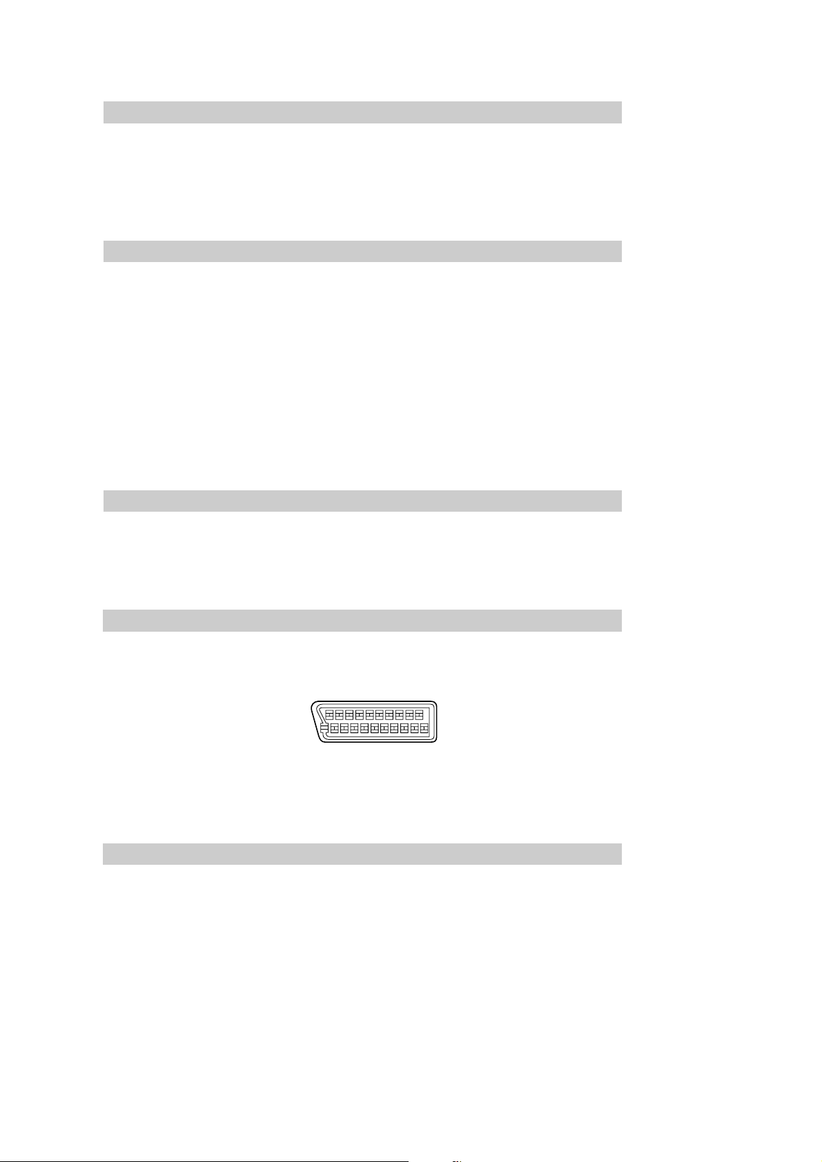
21-PIN CONNECTOR ASSIGNMENT
AV connector output ...................................................................................................... 21-pin connector
This connector provides the video and audio signals for connection to a compatible color TV or monitor.
20 18 16 14 12 10 8 6 4 2
21 19 17 15 13 11 9 7 5 3 1
PI N no.
1. Audio R out 8. Status 17. GND
3. Audio L out 11. G out 19. Video out
4. GND 15. R out 21. GND
7. B out 16. RGB SW
ACCESSORIES
Remote control unit (RC2400DV)........................................................................................................... 1
Batteries (AAA type) ............................................................................................................................... 2
Audio cable (Red/White) ........................................................................................................................ 1
Video cable (Yellow) ............................................................................................................................... 1
Coaxial cable (Black).............................................................................................................................. 1
Remote cable (Orange) .......................................................................................................................... 1
AC power cord........................................................................................................................................ 1
Registration card .................................................................................................................................... 1
User’s guide ........................................................................................................................................... 1
1
Page 4
2. CONNECTION FACILITIES
2.1 Video performance (/N only)
135791113151719
21
2. 1. 1 SCART
2 4 6 8 10 12 14 16 18 20
Pin No. TV (OUT) Pin No. AUX (IN)
Pin 1 Audio R out : 2Vrms Pin 1 Audio R out : 2Vrms
Pin 2 Audio R in : 2Vrms Pin 2 Audio R in : 2Vrms
Pin 3 Audio L out : 2Vrms Pin 3 Audio L out : 2Vrms
Pin 4 GND Pin 4 GND
Pin 5 GND Pin 5 GND
Pin 6 Audio L in : 2Vrms Pin 6 Audio L in : 2Vrms
Pin 7 Blue out/C in Pin 7 Blue in/C out
Pin 8 function switching out <2V : TV Pin 8 function switching in<2V : DVD
Pin 9 GND Pin 9 GND
Pin 10 not connected Pin 10 not connected
Pin 11 Green out:0.7Vpp ±0.1V into 75 Ohm *1 Pin 11 Green in:0.7Vpp ±0.1V into 75 Ohm
Pin 12 not connected Pin 12 not connected
Pin 13 GND Pin 13 GND
Pin 14 GND Pin 14 GND
Pin 15 Red/C out Pin 15 Red/C in
Pin 16 fast switching out <0.4V into 75 Ohm=CVBS/S-Video Pin 16 fast switching in <0.4V into 75 Ohm=CVBS/S-Video
1</<3 into 75 Ohm=RGB 1</<3 into 75 Ohm=RGB
Pin 17 GND Pin 17 GND
Pin 18 GND Pin 18 GND
Pin 19 CVBS/Y out : 1Vpp ±0.1V *1 Pin 19 CVBS/Y out : 1Vpp ±0.1V *1
Pin 20 CVBS/Y in : 1Vpp ±0.1V *1 Pin 20 CVBS/Y in : 1Vpp ±0.1V *1
Pin 21 GND Pin 21 GND
Blue : 0.7Vpp ±0.1V into 75 Ohm *1 Blue : 0.7Vpp ±0.1V into 75 Ohm *1
C : 300mVpp ±30 into 75 Ohm *2 C : 300mVpp ±30 into 75 Ohm *2
>5/<8 : asp.ratio 16 : 9 DVD/AUX >5/<8 : asp.ratio 16 : 9 AUX
>9.5/<12 : asp.ratio 4 : 3 DVD/AUX >9.5/<12 : asp.ratio 4 : 3 AUX
Red : 0.7Vpp ±0.1V into 75 Ohm *1 Red : 0.7Vpp ±0.1V into 75 Ohm *1
C : 300mVpp ±30 into 75 Ohm *2 C : 300mVpp ±30 into 75 Ohm *2
*1 : 100% White *2 : Burst Level *3 : color bar(chroma level : 75%)
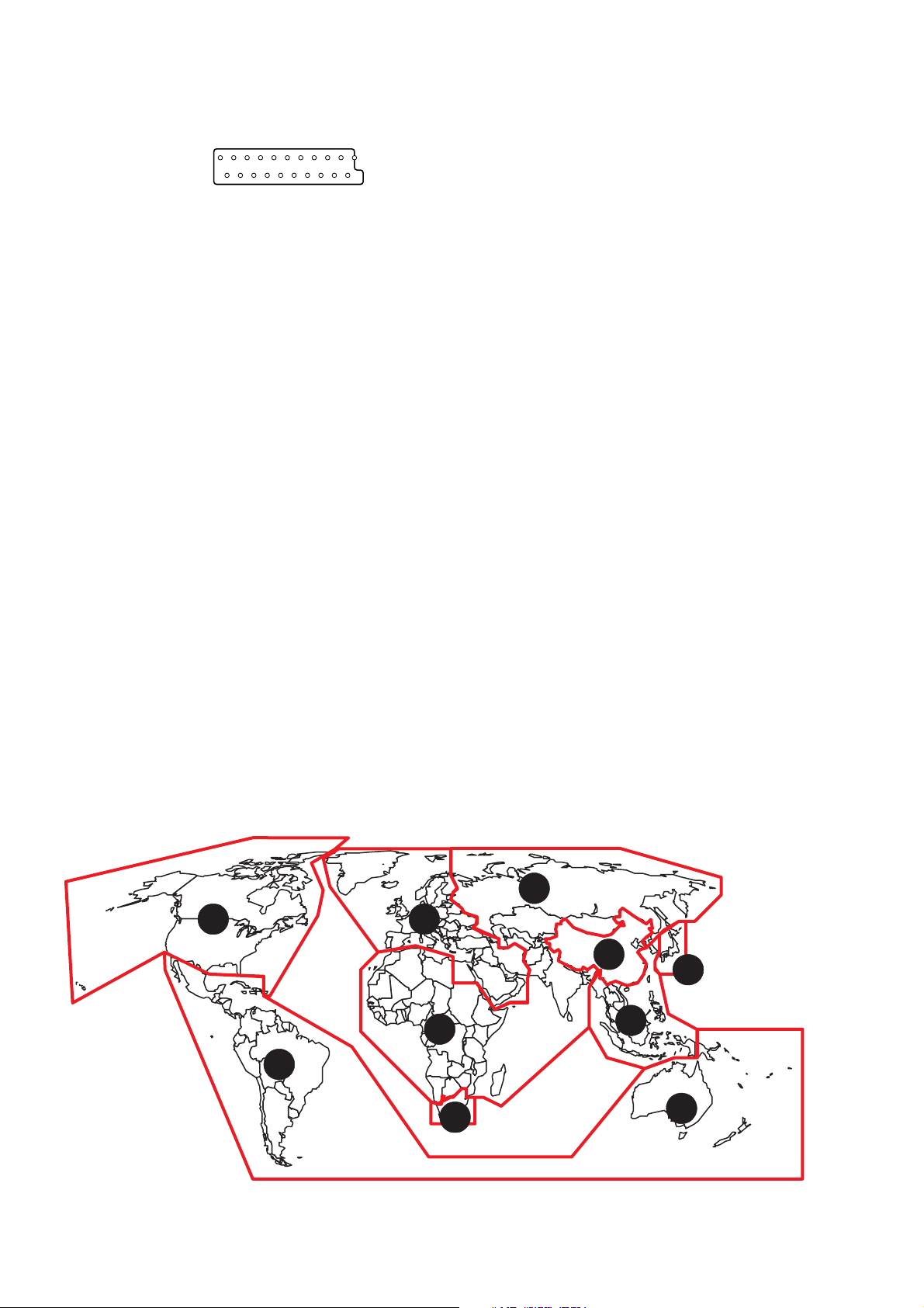
What are "regional codes"?
Motion picture studios want to control the home release of movies in different countries because theater releases arenit
simultaneous (a movie may come out on DVD in the US when itis just hitting screens in Europe). Therefore they have
required that the DVD standard include codes which can be used to lock out the playback of certain discs in certain geographical regions. Players sold in each region will have that regionis code built into the player. The player will refuse to play
these "region coded" discs which are not allowed in the region. However, regional codes are entirely optional. Discs without
codes will play on any player in any country. Some studios have already announced that only their new releases will have
regional codes. There are six regions:
1. United States and Canada 2. Europe and Japan
3. Far East (except Japan & China) 4. South America and Oceania
5. Africa and the Middle East 6. China (except Hong Kong)
5
1 2
6
2
5
3
4
2
Map of DVD Regions
2
4
Page 5
3. INFORMATIONS
ABOUT DISCS
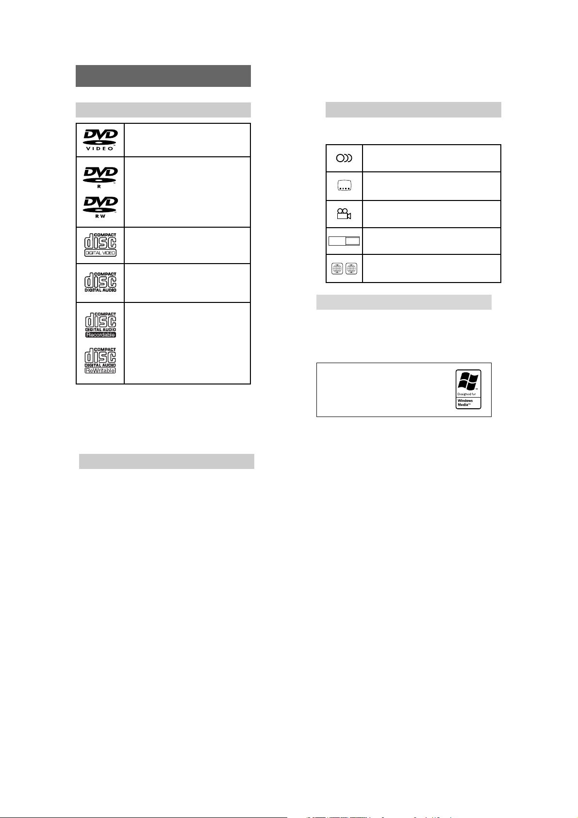
PLAYABLE DISCS
DVD
DVD-R/DVD-RW
Finalized DVD disc recorded in
the DVD video format.
Video CD (VCD) /
Super Video CD(SVCD)
Audio CD (CD-DA)
CD-R/CD-RW
Finalized CD-R and CD-RW
discs recorded in the CD-DA
format, MP3 format (
“ABOUT MP3/WMA”) or VideoCD format can be played with
the unit.
* Finalize is the process to make a DVD-R/DVD-
RW or CD-R/CD-RW playable for players (not
recorders)
* Some discs may not be able to be played
depending on condition of the discs.
☞ p3
ABOUT DVD DISCS
Marks on packages
The marks listed below indicate contents in a disc.
Indicates the number of recorded
2
audio tracks.
Indicates the number of recorded
2
subtitle languages.
Indicates the number of recorded
4
angles.
16 : 9LB
2
Indicates the selectable aspect
ratios.
Indicates the region number of the
ALL
disc.
ABOUT MP3/WMA
MP3 is the compressed music file in MPEG1, Audio
Layer 3 format.
An WMA(Windows Media Audio) file is a Microsoft
audio compression technology. WMA offers double
the audio compression of the MP3 format.
Microsoft, Windows Media, and the
Windows Logo are trademarks or
registered trademarks of Microsoft
Corporation in both the United
States and other countries.
NOT PLAYABLE DISCS
• DVD discs whose region number is not “2” nor
“ALL”.
• DVD-ROM
• DVD-RAM
• DVD-Audio
• CD-ROM
• CDV
• CD-G
• CVD
• Super Audio CD
• CD Photo, etc.
Caution
Some copy-controlled CDs may not conform to
offticial CD standards. They are special discs
and may not play on the DV2400.
3
Page 6
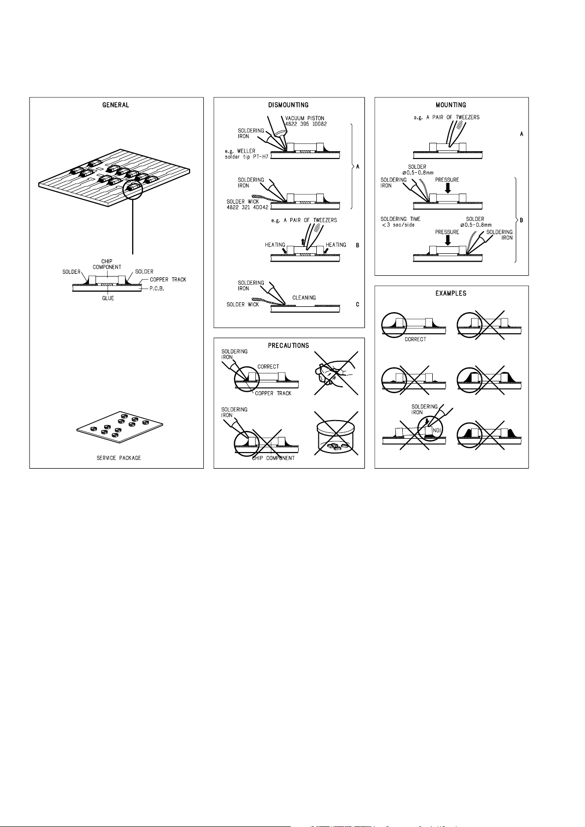
4. SERVICE HINTS AND TOOLS
SERVICE HINTS
SERVICE TOOLS
Audio signals disc 4822 397 30184
Disc without errors (SBC444)+
Disc with DO errors, black spots and fingerprints (SBC444A) 4822 397 30245
Disc (65 min 1kHz) without no pause 4822 397 30155
Max. diameter disc (58.0 mm) 4822 397 60141
Torx screwdrivers
Set (straight) 4822 395 50145
Set (square) 4822 395 50132
13th order filter 4822 395 30204
DVD test disc (PAL) 4822 397 10131
DVD test disc (NTSC) ALMEDIO TDV-540
4
Page 7
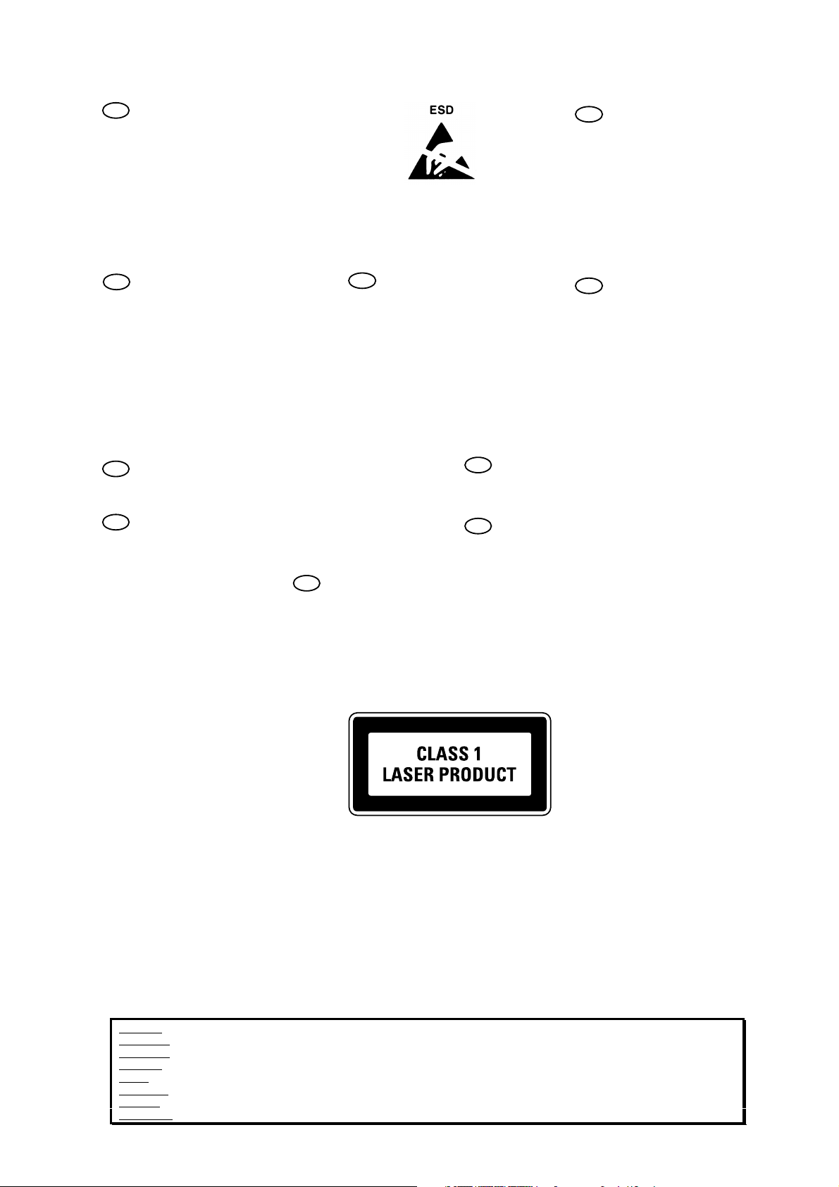
5. WARNING AND LASER SAFETY INSTRUCTIONS
GB
WARNING
All ICs and many other semi-conductors are
susceptible to electrostatic discharges (ESD).
Careless handling during repair can reduce
life drastically.
When repairing, make sure that you are
connected with the same potential as the
mass of the set via a wrist wrap with
resistance.
Keep components and tools also at this
potential.
F
ATTENTION
D
WARNUNG
I
WAARSCHUWING
AVVERTIMENTO
NL
Alle IC’s en vele andere halfgeleiders zijn
gevoelig voor elektrostatische ontladingen
(ESD).
Onzorgvuldig behandelen tijdens reparatie
kan de levensduur drastisch doen
verminderen.
Zorg ervoor dat u tijdens reparatie via een
polsband met weerstand verbonden bent met
hetzelfde potentiaal als de massa van het
apparaat.
Houd componenten en hulpmiddelen ook op
ditzelfde potentiaal.
Tous les IC et beaucoup d’autres semiconducteurs sont sensibles aux décharges
statiques (ESD).
Leur longévité pourrait être considérablement
écourtée par le fait qu’aucune précaution
n’est prise a leur manipulation.
Lors de réparations, s’assurer de bien être
relié au même potentiel que la masse de
l’appareil et enfiler le bracelet serti d’une
résistance de sécurité.
Veiller a ce que les composants ainsi que les
outils que l’on utilise soient également a ce
potentiel.
GB
Safety regulations require that the set be restored to its original condition
and that parts which are identical with those specified be used.
NL
Veiligheidsbepalingen vereisen, dat het apparaat in zijn oorspronkelijke
toestand wordt terug gebracht en dat onderdelen, identiek aan de
gespecifieerde worden toegepast.
Alle IC und viele andere Halbleiter sind
empfindlich gegen elektrostatische
Entladungen (ESD).
Unsorgfältige Behandlung bei der Reparatur
kann die Lebensdauer drastisch vermindern.
Sorgen sie dafür, das Sie im Reparaturfall
über ein Pulsarmband mit Widerstand mit
dem Massepotential des Gerätes verbunden
sind.
Halten Sie Bauteile und Hilfsmittel ebenfalls
auf diesem Potential.
D
Bei jeder Reparatur sind die geltenden Sicherheitsvorschriften zu beachten.
Der Originalzustand des Gerats darf nicht verandert werden.
Fur Reparaturen sind Original-Ersatzteile zu verwenden.
I
Le norme di sicurezza esigono che l’apparecchio venga rimesso nelle
condizioni originali e che siano utilizzati pezzi di ricambiago idetici a quelli
specificati.
Tutti IC e parecchi semi-conduttori sono
sensibili alle scariche statiche (ESD).
La loro longevita potrebbe essere fortemente
ridatta in caso di non osservazione della piu
grande cauzione alla loro manipolazione.
Durante le riparazioni occorre quindi essere
collegato allo stesso potenziale che quello
della massa dell’apparecchio tramite un
braccialetto a resistenza.
Assicurarsi che i componenti e anche gli
utensili con quali si lavora siano anche a
questo potenziale.
F
“Pour votre sécurité, ces documents
doivent être utilisés par des
spécialistes agrées, seuls habilités à
réparer votre appareil en panne.”
Les normes de sécurité exigent que l’appareil soit remis a l’état d’origine et
que soient utilisées les pièces de rechange identiques à celles spécifiées.
LASER SAFETY
This unit employs a laser. Only a qualified service person should remove the cover or attempt to service this
device, due to possible eye injury.
USE OF CONTROLS OR ADJUSTMENTS OR PERFORMANCE OF PROCEDURE OTHER THAN THOSE
SPECIFIED HEREIN MAY RESULT IN HAZARDOUS RADIATION EXPOSURE.
AVOID DIRECT EXPOSURE TO BEAM
WARNING
The use of optical instruments with this product will increase eye hazard.
Repair handling should take place as much as possible with a disc loaded inside the player
WARNING LOCATION: INSIDE ON LASER COVERSHIELD
CAUTION VISIBLE AND INVISIBLE LASER RADIATION WHEN OPEN AVOID EXPOSURE TO BEAM
ADVARSEL SYNLIG OG USYNLIG LASERSTRÅLING VED ÅBNING UNDGÅ UDS
ADVARSEL SYNLIG OG USYNLIG LASERSTRÅLING NÅR DEKSEL Å PNES UNNGÅ EKSPONERING FOR STRÅLEN
VARNING SYNLIG OCH OSYNLIG LASERSTRÅLNING NÄR DENNA DEL ÄR ÖPPNAD BETRAKTA EJ STRÅLEN
VARO! AVATT AESSA OLET ALTTIINA NÄKYVÄLLE JA NÄKYMÄTTÖMÄLLE LASER SÄTEILYLLE. ÄLÄ KATSO SÄTEESEEN
VORSICHT SICHTBARE UND UNSICHTBARE LASERSTRAHLUNG WENN ABDECKUNG GEÖFFNET NICHT DEM STRAHL AUSSETSEN
DANGER VISIBLE AND INVISIBLE LASER RADIATION WHEN OPEN AVOID DIRECT EXPOSURE TO BEAM
ATTENTION RAYONNEMENT LASER VISIBLE ET INVISIBLE EN CAS D'OUVERTURE EXPOSITION DANGEREUSE AU FAISCEAU
Æ
TTELSE FOR STRÅLING
030804ecm
5
Page 8
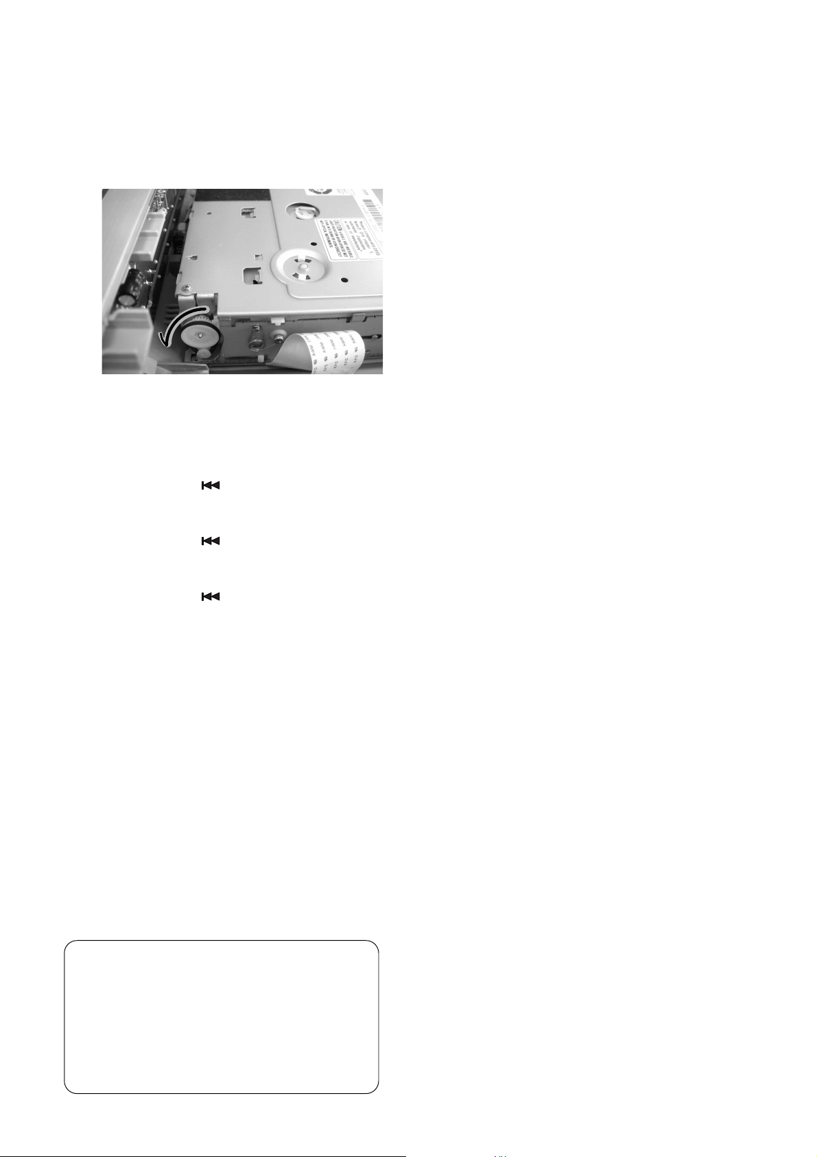
6. TAKING THE DISC OUT OF EMERGENCY
1. Remove 6 screws on the top cover and remove the top
cover.
2. Turn the gear to the direction with your fi nger.
3. The disc will out.
7. SERVICE MODE
[1] Micro-Processor (IC91: Front PCB) version
check
1. Power is STANDBY mode.
2. While pressing Previous and ENTER button on the
remote controller over 3 sec.
3. The FLD segments light up one by one.
4. While pressing Previous and ENTER button again
over 3 sec.
5. The FLD segments stops in the light up position.
6. While pressing Previous and ENTER button again
over 3 sec.
7. Micro-Processor version is displayed on the front FLD.
(Ex.: 2003 10 11)
8. Turn off the power to quit Service Mode.
[2] Firmware (Front-end and Back-end : DVD
MECHA PCB MODULE) version check
Connect the DVD player to [TV] and operate by using
[Remote controller RC2400DV]
1. Press the POWER button to turn on the unit. "NO DISC" is
displayed on the front FLD.
2. Press the CLEAR button on the remote controller and press
2, 5, 8, 0 and press CLEAR button again.
3. The following information is displayed on the TV screen.
The fi rmware version is shown
(Ex.: BE VER MZA20022
FE VER GB14 031011A0)
[3] Software update
Connect the DVD player to [TV] and operate by using
[Remote controller RC2400DV]
1. How to update for Front-end by update DISC.
1) Press the POWER button to turn on the unit. "NO DISC"
is displayed on the front FLD.
2) Insert the update CD-ROM (part no.*DV24001CR) in the
DISC slot.
3) Software updating will be done automatically. When the
updating is fi nished, the update CD-ROM is ejected automatically.
4) Remove CD-ROM.
5) Wait until "EJECT" is displayed on the TV screen. ("DISC
LOADING" then "EJECT" then "NO DISC" are displayed
on the TV screen. It takes about 15 seconds for displayed
as EJECT)
6) The software has been updated.
7) Turn off power to quit SERVICE MODE.
Cautions; When interrupted, redo from the start agein
2. How to update for Back-end by update DISC.
1) Press the POWER button to turn on the unit. "NO DISC"
is displayed on the front FLD
2) Press the CLEAR button on the remote controller and
press 2, 5, 8, 0 and press CLEAR button again. "TEST-
MODE" is displayed on the front FLD
3) Insert the update CD-ROM (part no.*DV24002CR) in the
DISC slot half.
4) Press the PROGRAM button. The disc is automatically
inserted in the unit.
5) Software updating will be done automatically. ("ERASE
>>>>>>>>>>" then "WRITE >>>>>>>>>" then "DONE"
are displayed on the TV screen.)
7) When the updating is fi nished, the unit becomes automatic at standby mode.
8) Press the POWER button to turn on the unit
9) Press the EJECT button then remove CD-ROM.
10)The software has been updated.
11)Turn off power to quit SERVICE MODE.
Cautions; When interrupted, please redo from the start
again.
• Firmware update CD-ROM for Front-end ....*DV24001CR
• Firmware update CD-ROM for Back-end ....*DV24002CR
CH I P I D T VERS I ON 31
BE VER MZA20022/ PAL/
BUI LD T IME 031104
FE VER GB14 031011A
0
DEFAUL T TV 4 : 3 LB / PAL
PLAYABEL D I SC VCD+MP3
00: 4D5A4132303032 32
08:FFFFFFFF737300
3
4
W
0
6
Page 9
8. WIRING DIAGRAM
HJDRL - ASL820
CUP11670Z CUP11673Z
CUP11609Z
CUP11645Z
7 8
Page 10
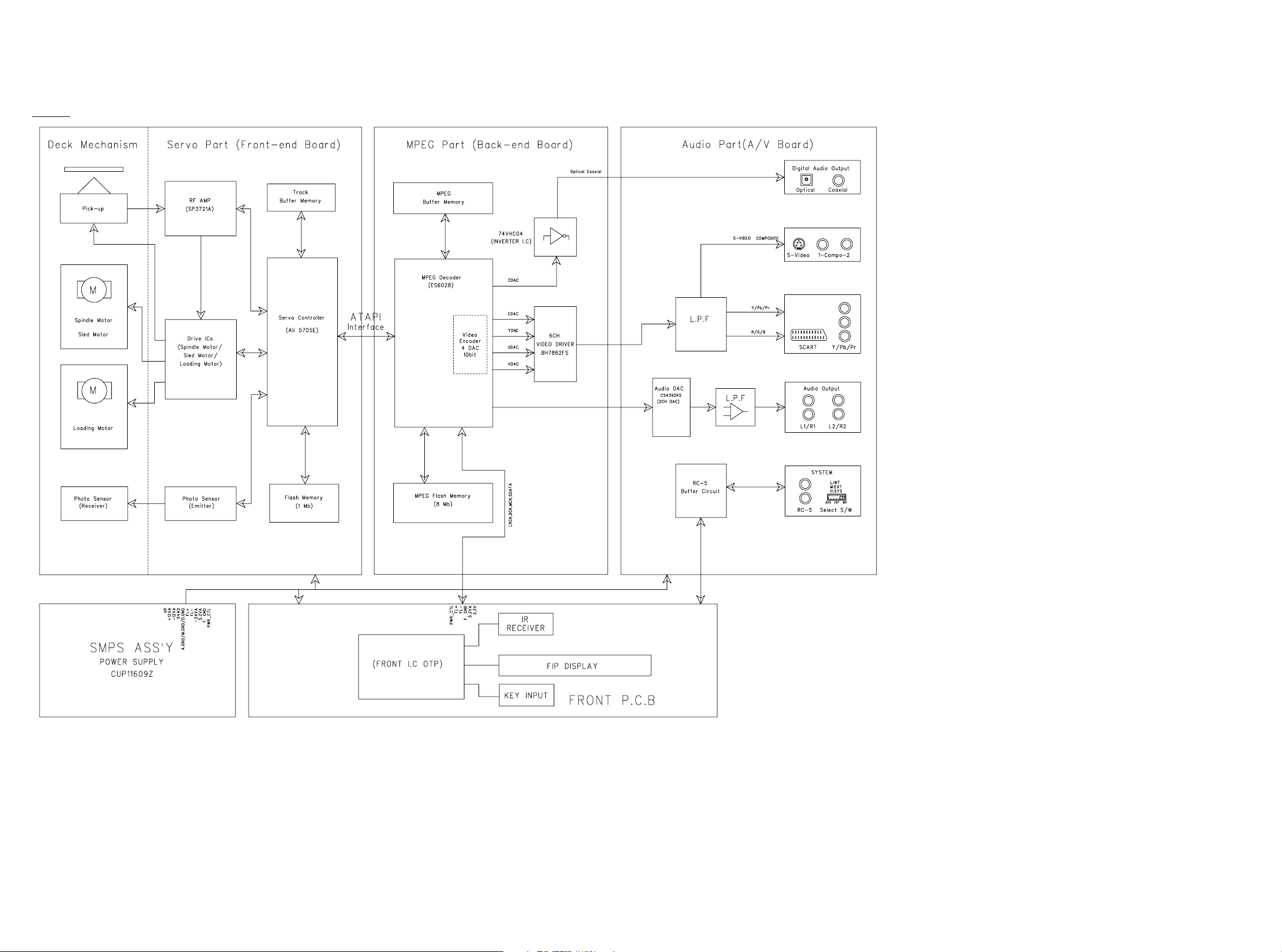
9. BLOCK DIAGRAM
N only
109
Page 11
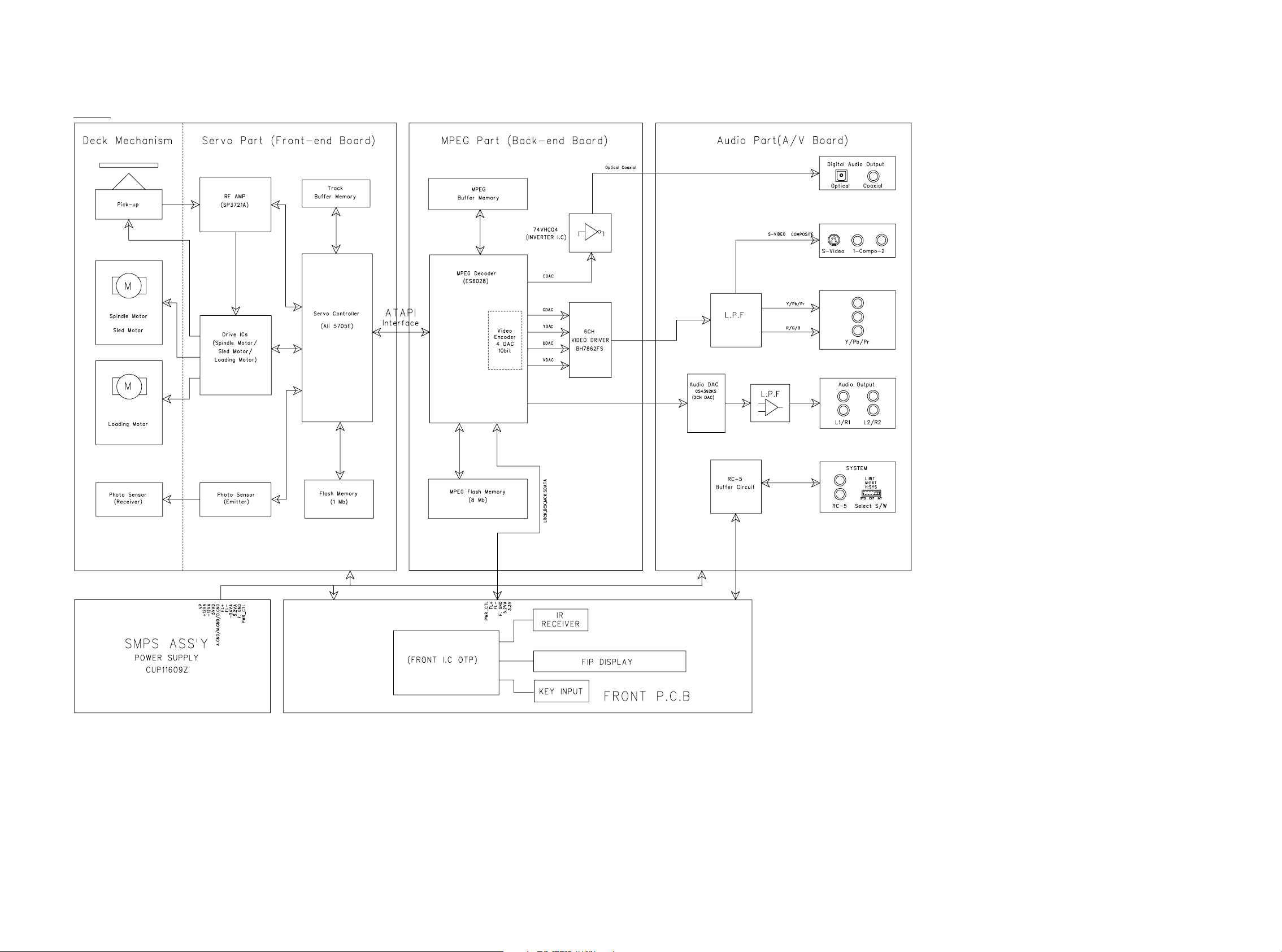
S only
11 12
Page 12
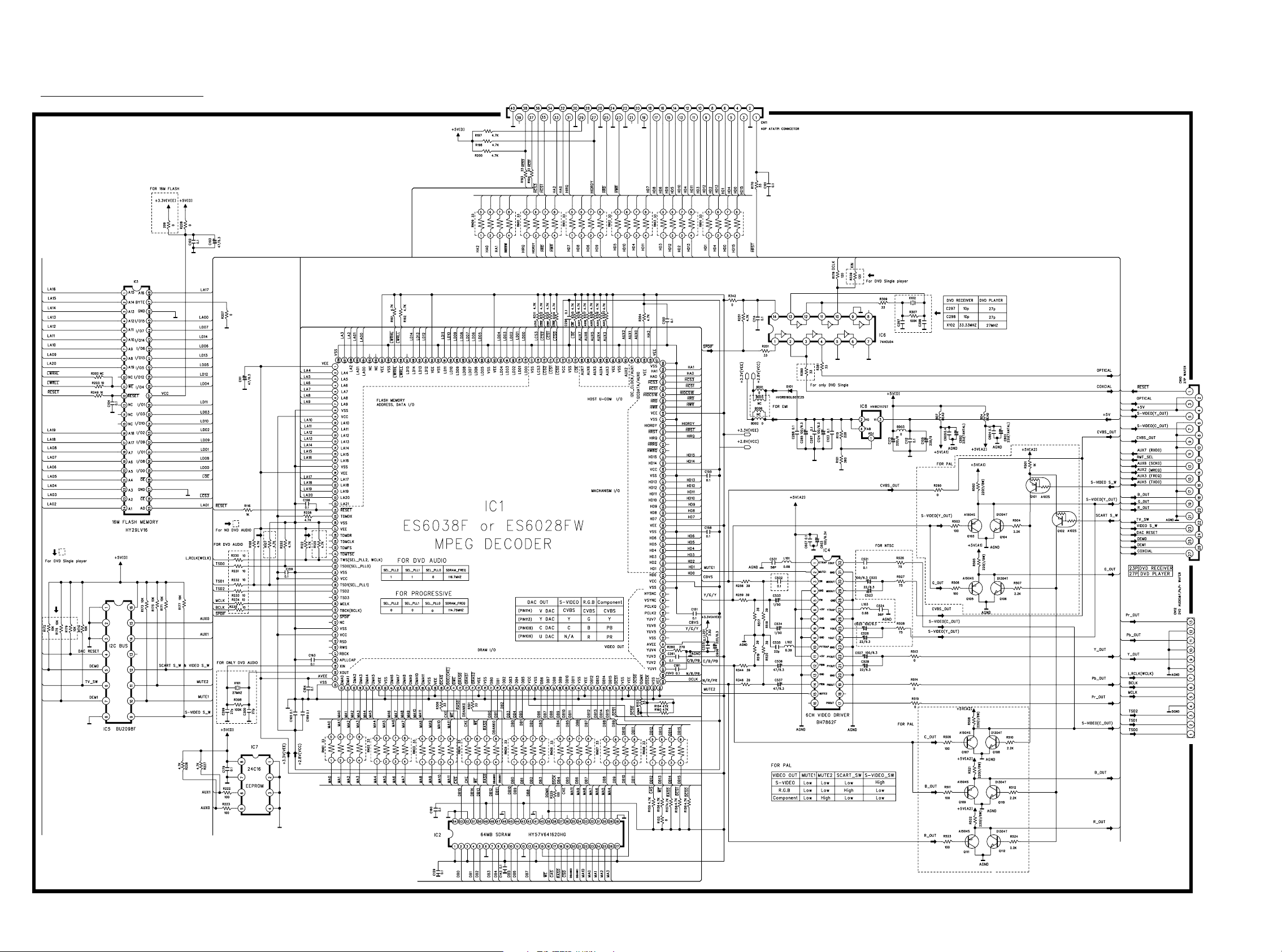
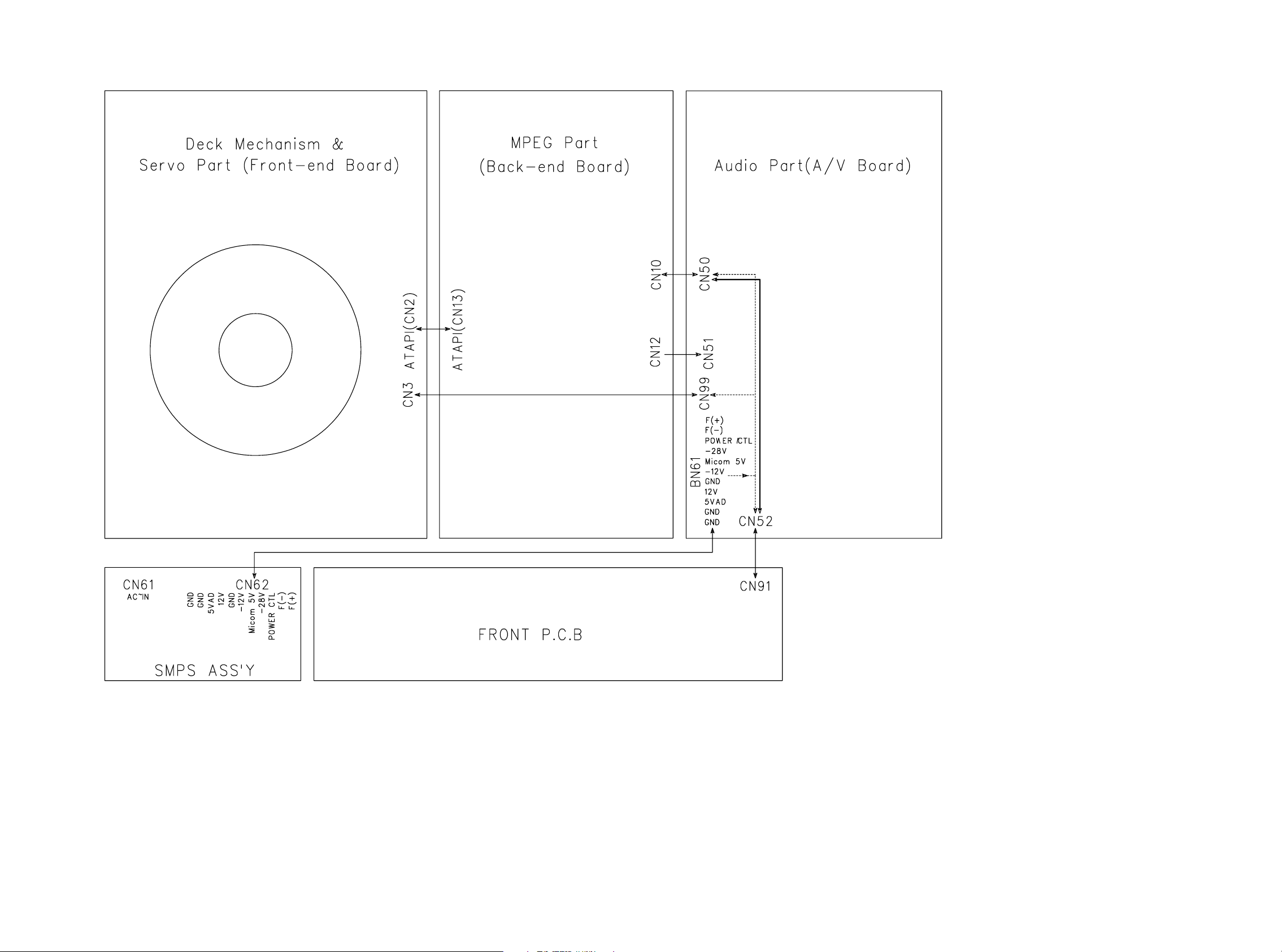
10. SCHEMATIC DIAGRAM
BACK-END PCB MPEG Part
1413
Page 13

A/V PCB Audio Part
15 16
Page 14

FRONT PCB Front Part
1817
Page 15

SMPS ASS’Y
19 20
Page 16

11. PARTS LOCATION
FRONT
Q901 Q910 Q908 - Q905 Q912 Q913
Q904
Q902
Q903 Q915 Q914
Q909 Q911IC92
FRONT
IC93
IC91
2221
Page 17

A/V
IC54 IC53
Q602
Q603
Q604
Q607
Q616
Q617
Q618
Q601
Q619
Q620
Q606
Q605
Q610
Q611
Q608
Q609
Q613
Q615
Q614
Q612
23
Page 18

A/V
IC51
IC52
24
Page 19

BACK - END (DVD MPEG)
IC6
IC2
IC1
IC7
IC5
IC8
Q102
Q111 Q107
Q101
Q112 Q108
IC3
IC4
Q105 Q103
Q106 Q104
Q109
Q110
25
Page 20

BACK - END (DVD MPEG)
26
Page 21

12. MICROPROCESSOR AND IC DATA
IC4:BH7862FS
Pin No. Pin name Pin descriptionInput/output equivalent circuit
CIN
3
PbIN
12
PrIN
14
20k
Signal input terminal.
Input terminal for chroma signal and color-difference
signal.
Bias type input.
The input impedance is 20kΩ.
MUTE1
CIN
GND
YIN
V
GND
PYIN
GND
PYTRAP
V
PbIN
GND
1
32
COUTCTRAP
75Ω6dB
2
3
4
5
6
CC
MUTE1 TEST
20k
1.5-6M
BPF
6M
LPF
75Ω6dB
31
30
29
28
27
TEST
MIXOUT
MIXFB
GND
YTRAP
58YIN
PYIN
32 COUT
2930MIXFB
MIXOUT
Signal input terminal.
Input terminal for luminance signal.
Di clamp input.
Signal output terminal.
Output terminal for chroma signal.
Signal output terminal.
Output terminal for Y/C MIX signal.
CLAMP
7
8
CLAMP
12M
LPF
75Ω6dB
9
10
CC
11
12
20k
6M
LPF
75Ω6dB
13
26
25
24
23
22
21
20
GND
YOUT
YFB
GND
PYOUT
PYFB
GND
24
YFB
25
YOUT
Pin No. Pin name Pin descriptionInput/output equivalent circuit
2122PYFB
PYOUT
1719PrOUT
PbOUT
Signal output terminal.
Output terminal for luminance signal (interlaced type).
Signal output terminal.
Output terminal for luminance signal
(progressive type).
Signal output terminal.
Output terminal for color-difference signal.
PrIN
MUTE2
PrTRAP
14
15
16
20k
MUTE2
6M
LPF
75Ω6dB
75Ω6dB
19
18
17
PbOUT
CTPAP
1
YTRAP
27
PYTRAP
10
PrTRAP
16
N.C.
6
V
PrOUT
Pin No. Pin name Pin descriptionInput/output equivalent circuit
12 MUTE2
31 TEST
18 N.C.
11
4
7
9
13
20
23
26
28
2 MUTE1
CC
GND
Terminal for LC resonance.
Power supply voltage.
CC
is separated into 6 pin and 11 pin.
V
That is to say, C, MIX and Y are partitioned by 6 pin
and PY, Pb and Pr by 11 pin.
They and not connected internally.
Connect them externally when using.
Grounding terminal.
Mute control terminal.
C, MIX and Y are muted simultaneously by setting
MUTE to "L".
Mute control terminal.
PY, Pb and PR are muted simultaneously by setting
MUTE to "L".
Test terminal.
Usually, short-circuit this terminal to GND when using it.
27
Page 22

IC7:BR24C16
1
A0
A1
2
A2
3
HIGH VOLTAGE GEN.
4
GND
IC5:BU2098F-J
SDA
SCL
A0
A1
A2
16kbits EEPROM ARRAY
11bits
ADDRESS
11bits
DECODER
START STOP
CONTROL LOGIC
Power-On Reset
2
C BUS
I
Controller
SLAVE WORD
·
ADDRESS REGISTER
VCC LEVEL DETECT
REGISTER
ACK
Shift
Register
8bits
DATA
8bit
V
CC
8
V
GND
A0, A1, A2
SCL
SDA
7
WP
SCL
6
WP
SDA
5
L
a
Write
t
Buffer
c
h
An open drain output requires a pull-up resistor.
I / O
CC
Power supply
FunctionPin name
Ground (0V)
I
Out of use. Please connect to GND.
Serial clock input
I
Slave and word address,
I / O
serial data input, serial data output
Wite protect pin
I
Q7
Q6
Q5
Q4
Q3
Q2
Q1
Q0
4~7
13
14
15
16
9~12
8
A0
1
A1
A2
Q0
Q1
Q2
Q3
VSS
Pin namePin No. Type Function
(pull-up is being done inside)
Q0~Q7
SS
V
NC
SCL
SDA
DD
V
O
I / O
I1~3 A0~A2
Input of an address
Open Dorain output
-
GND
N.C.
Cereal clock input
I
Cereal data input / output
-
Power supply
DD
V
SDA
SCL
NC
Q7
Q6
Q5
Q4
28
Page 23

IC51:CS4392-2
M1
(SDA/CDIN)
M2
(SCL/CCLK) (AD0/CS)
M3
M0
AMUTEC
CMOUT
FILT+BMUTEC
RST
SCLK
LRCK
SDATA
RST AMUTEC
VL AOUTA-
SDATA AOUTA+
SCLK VA
LRCK AGND
MCLK AOUTB+
M3 AOUTB-
(SCL/CCLK) M2 BMUTEC
(SDA/CDIN) M1 CMOUT
(AD0/CS
)M0 FILT+
1
2
3
4
5
6
7
8
9
10
20
19
18
17
16
15
14
13
12
11
SERIAL
PORT
MODE SELECT
(CONTROL PORT)
VOLUME
CONTROL
MIXER
VOLUME
CONTROL
MUTE CONTROL
INTERPOLATION
FILTER
INTERPOLATOR
FILTER
EXTERNAL
MCLK
∆∑
DAC
∆∑
DAC
REFERENCE
ANAL OG
FILTER
ANAL OG
FILTER
AOUTA+
AOUTA-
AOUTB+
AOUTB-
RST 1 Reset (Input) - Powers down device and resets all internal registers to their default settings.
VL 2 Logic Power (Input) - Positive power for the digital input/output.
SDATA 3 Serial Audio Data (Input) - Input for two’s complement serial audio data.
SCLK 4 Serial Clock (Input/Output) - Serial clock for the serial audio interface.
LRCK 5 Left Right Clock (Input/Output) - Determines which channel, Left or Right, is currently active on the
serial audio data line.
MCLK 6 Master Clock (Input) - Clock source for the delta-sigma modulator and digital filters.
FILT+ 11 Positive Voltage Reference (Output) - Positive reference voltage for the internal sampling circuits.
CMOUT 12 Common Mode Voltage (Output) - Filter connection for internal quiescent voltage.
AMUTEC
BMUTEC
AOUTB-
AOUTB+
AOUTA+
AOUTA
20
13
14
15
18
19
Mute Control (Output) - The Mute Control pin goes high during power-up initialization, reset, muting,
power-down or if the master clock to left/right clock frequency ratio is incorrect.
Differential Analog Output (Outputs) - The full scale differential analog output level is specified in the
Analog Characteristics specification table.
AGND 16 Ground (Input)
VA
17 Analog Power (Input) - Positive power for the analog section.
Control Port Mode Definitions
M3
SCL/CCLK 8
SDA/CDIN 9 Serial Control Data (Input/Output) - SDA is a data I/O line in I
7 Mode Selection (Input) - This pins should be tied to GND level during control port mode.
Serial Control Port Clock (Input) - Serial clock for the serial control port.
2
C mode. CDIN is the input data line for
the control port interface in SPI mode.
AD0/CS
10 Address Bit 0 (I2C) / Control Port Chip Select (SPI) (Input/Output) - AD0 is a chip address pin in I2C
mode; CS
is the chip select signal for SPI format.
Stand-Alone Mode Definitions
Mode Selection (Input) - Determines the operational mode of the device.
M3
M2
M1
M0
7
8
9
10
29
Page 24

IC91:GMS81C2020
ADC Power
Supply
SS
AVDDAV
Driver
Buzzer
R07
R06
R05
R04
R03/BUZO
R02/EC0
R01/INT1
R00/INT0
R0
R10~R17
R1
R20~R27
R2
R30~R35
R3
Vdisp/RA
RA
PSW
Syst
em controller
System
Clock Controller
Sub System
Clock Controller
Timing generator
Clock
Generator
IN
X
OUT
X
RESET
High Voltage Port
IN
SX
ALU
8-bit Basic
Interv al
Timer
Watchdog
OUT
SX
Power
Supply
A
Interrupt Controller
8-bit
Timer/
Counter
Timer
R4 R5
R40 / T0O
R41
SS
DD
V
V
R42
R43 R73 / AN11
X Y
Stack Pointer
8-bit serial
Interface
Data Memory
10-bit
PWM
R50
R51
R52
R53 / SCLK
R54 / SIN
R55 / SOUT
R56 / PWM1O/T1O
R57
(448 bytes)
8-bit
ADC
Data Table
R6
R60 / AN0
R61 / AN1
R62 / AN2
R63 / AN3
R64 / AN4
R65 / AN5
R66 / AN6
R67 / AN7
PC
Program
Memory
PC
R7
R70 / AN8
R71 / AN9
R72 / AN10
Pin No. Symbol Description
1 AMUTE AMUTE
2 SCKO SCKO
3 TXDO TXDO
4 RXDO RXDO
5~6 No Connect -
7 RESET RESET
8 XI 4MHz Crystal Connection port
9XO
10 VSS GND
11~12 No Connect -
13 AVSS GND
14 KEY IN #1 -
15~19 No Connect -
20 (VFD)DATA_OUT
21 (VFD)CLK VFD Control Port
22 (VFD)CSB
23 INT/EXT/SYS SEL INT/EXT/SYS Select Port
24~25 3.3V 3.3V
26 AVDD 3.3V
27 VDD 3.3V
28 M_REQ M_REQ Port
29 REMOTE_IN Remocon Censor Control
30 REMOTE_OUT
31 IR NOR/KILL IR NOR/KILL
32~60 No Connect -
61 M_RESET M_RESET Port
62 PWR_CTL Power Control Port
63 F_REQ F_REQ Port
64 No Connect -
30
Page 25

IC1:ES6028
TSD0
33
O Audio transmit serial data port 0.
SEL_PLL0 I Refer to the description and matrix for SEL_PLL2 pin 32.
TSD1
36
O Audio transmit serial data port 1.
SEL_PLL1 I Refer to the description and matrix for SEL_PLL2 pin 32.
TSD2 37 O Audio transmit serial data port 2.
NC 38, 42, 48 — No connect pins. Leave open.
MCLK 39 I/O Audio master clock for audio DAC.
TBCK 40 O Audio transmit bit clock.
SPDIF
41
O S/PDIF output.
SEL_PLL3
I Clock source select.Strapped to VCC or ground via 4.7-kΩ resistor; read only
during reset.
RSD 45 I Audio receive serial data.
RWS 46 I Audio receive frame sync.
RBCK 47 I Audio receive bit clock.
XIN 49 I 27-MHz crystal input.
XOUT 50 O 27-MHz crystal output.
AVEE 51 I Analog power for PLL.
DMA[11:0] 53:58, 61:66 O DRAM address bus.
DCAS# 69 O DRAM column address strobe.
DOE#
70
O DRAM output enable.
DSCK_EN O DRAM clock enable.
DWE# 71 O DRAM write enable.
DRAS# 72 O DRAM row address strobe.
DMBS0 73 O SDRAM bank select 0.
DMBS1 74 O SDRAM bank select 1.
DB[15:0] 77:82, 85:90, 93:96 I/O DRAM data bus.
DCS[1:0]# 97,100 O SDRAM chip select.
DQM 101 O Data input/output mask.
DSCK 102 O Output clock to SDRAM.
DCLK 105 I Clock input to PLL.
Table 1 ES6028 Pin Description (Continued)
Name Pin Numbers I/O Definition
SEL_PLL3 Clock Source
0 Crystal oscillator
1 DCLK input
YUV6
114
O YUV6 pix el output data.
VDAC O Video DAC output. Refer to description and matrix for UDAC pin 106.
YUV7
115
O YUV7 pix el output data.
CAMIN3 I Camera YUV 3.
PCLK2XSCN
116
I/O 27-MHz video output pixel clock.
CAMIN4 I Camera YUV 4.
PCLKQSCN
117
O 13.5-MHz video output pixel clock.
CAMIN5 I Camera YUV 5.
AUX3[2] I/O Aux3 data I/O.
VSYNC#
118
I/O Vertical sync, active-low.
CAMIN6 I Camera YUV 6.
AUX3[1] I/O Aux3 data I/O.
HSYNC#
119
I/O Horizontal sync, active-low.
CAMIN7 I Camera YUV 7.
AUX3[0] I/O Aux3 data I/O.
HD[5:0]
122:127
I/O Host data bus lines 5:0.
DCI[5:0] I/O DVD channel data I/O.
AUX1[5:0] I/O Aux1 data I/O.
HD[6]
128
I/O Host data bus line 6.
DCI[6] I/O DVD channel data I/O.
AUX1[6] I/O Aux1 data I/O.
VFD_DOUT I VFD data output.
HD[7]
131
I/O Host data bus line 7.
DCI[7] I/O DVD channel data I/O.
AUX1[7] I/O Aux1 data I/O.
VFD_DIN I VFD data input.
HD[8]
132
I/O Host data bus line 8.
DCI_FDS# I/O DVD input sector start.
AUX2[0] I/O Aux2 data I/O.
VFD_CLK I VFD clock input.
HD[9]
133
I/O Host data bus line 9.
AUX2[1] I/O Aux2 data I/O.
SQSQ I Subcode-Q data.
Table 1 ES6028 Pin Description (Continued)
Name Pin Numbers I/O Definition
HIOCS16#/CAMCLK/AUX3[4]
HA1/AUX4[3]
VSS
HA0/AUX4[2]
HWR#/DCI_CLK/AUX4[5]
HRD#/DCI_ACK#/AUX4[6]
VEE
HCS3FX#/AUX3[6]
HCS1FX#/AUX3[7]
VSS
HIORDY/AUX3[3]
HIRQ/DCI_ERR#/AUX4[7]
HRST#/AUX3[5]
HRRQ#/AUX4[0]
HWRQ#/DCI_REQ#/AUX4[1]
142
143
144
145
146
147
148
149
150
151
152
153
154
155
156
157
VEE
HA2
/AUX4[4]
I2CDATA/AUX[0]
I2C_CLK/AUX[1]
AUX[2]/IOW#
AUX[3]/IOR#
AUX[7]/STALL#
LWRLL#
LWRHL#
CAMIN0
CAMIN1
ES6028 PIN DESCRIPTION
Table 1 lists the pin descriptions for the ES6028.
Table 1 ES6028 Pin Description
Name Pin Numbers I/O Definition
VEE
LA[21:0]
VSS
VCC
RESET# 24 I Reset input, active-low.
TDMDX
RSEL
TDMDR 28 I TDM receive data input.
TDMCLK 29 I TDM clock input.
TDMFS 30 I TDM frame sync input.
TDMTSC# 31 O TDM output enable.
TWS
SEL_PLL2
158
159
VEE
160
161
162
163
VSS
164
VEE
165
166
AUX[4]
167
AUX[5]
168
AUX[6]
169
170
LOE#
171
VSS
172
VCC
173
LCS0#
174
LCS1#
175
LCS2#
176
LCS3#
177
VSS
178
LD0
LD1
179
LD2
180
LD3
181
LD4
182
VEE
183
184
VSS
LD5
185
LD6
186
LD7
187
LD8
188
LD9
189
LD10
190
LD11
191
VSS
192
VEE
193
LD12
194
LD13
195
LD14
196
LD15
197
198
199
VSS
200
VEE
201
202
203
LA0
204
LA1
205
LA2
206
LA3
207
VSS
208
1
VEE
1,18, 27, 59, 68, 75,
92, 99, 104, 130,
148, 157, 159, 164,
183, 193, 201
2:7, 10:16, 19:23,
204:207
8, 17, 26, 34, 43,
52, 60, 67, 76, 84,
91, 98, 103, 112,
120, 129, 138, 147,
156, 163, 171, 177,
184, 192, 200, 208
9, 35, 44, 83, 121,
139, 172
25
32
208-Pin PQFP Package
2 3 4 5 6 7 8 910111213141516171819202122232425262728293031323334353637383940414243444546474849505152
LA4
LA5
LA6
LA7
LA8
LA9
VSS
VCC
LA11
LA10
LA12
LA13
LA14
LA15
I I/O power supply.
O RISC port address bus.
I Ground.
I Core power supply.
O TDM transmit data output.
I LCS3 ROM Boot Data Width Select. Strapped to VCC or ground via 4.7-kΩ
resistor; read only during reset.
RSEL Selection
016-bit ROM
18-bit ROM
O Audio transmit frame sync output.
I System and DSCK output clock frequency s ele cti on i s made at the rising edge of
RESET#. The matrix below lists the available clock frequencies and their
respective PLL bit settings. Strapped to VCC or ground via 4.7-kΩ resistor; read
only during reset.
SEL_PLL2 SEL_PLL1 SEL_PLL0 Clock Type
0 0 0 DCL K x 4.25
0 0 1 Reserved
0 1 0 Bypass mode
0 1 1 DCL K x 3.75
1 0 0 DCL K x 4.5
1 0 1 Reserved
1 1 0 DCL K x 3.5
1 1 1 DCL K x 4
Table 1 ES6028 Pin Description (Continued)
Name Pin Numbers I/O Definition
HD[10]
AUX2[2] I/O Aux2 data I/O.
SQSK I Subcode-Q clock.
HD[11]
AUX2[3] I/O Aux2 data I/O.
IRQ O IRQ.
HD4/DCI4/AUX1[4]
HD5/DCI5/AUX1[5]
HD6/DCI6/AUX1[6]/VFD_DOUT
HD2/DCI2/AUX1[2]
VSS
HD13/AUX2 [5 ]/S P
HD12/AUX2[4]/C2PO
HD11/AUX2[3]//IRQ
HD10/AUX2 [2 ]/S QSK
HD9/AUX2[1]/SQSO
HD15/AUX2 [7 ]/IR
HD14/AUX2 [6 ]/S QSI
VCC
139
140
141
HD8/DCI_FDS#/AUX2[0]/VFD_CLk
132
133
134
135
136
137
138
ES6028F
VSS
VEE
LA16
LA17
VSS
LA18
LA19
LA21
LA20
RESET#
TDMDX/RSEL
HD3/DCI3/AUX1[3]
VSS
HD7/DCI7/AUX1[7]/VFD_DIN
VEE
130
131
VEE
TDMDR
HD1/DCI1/AUX1[1]
HD0/DCI0/AUX1[0]
VCC
VSS
HSYNC#/CAMIN7/AUX3[0]
PCLK2XSCN/CAMIN4
YUV7/CAMIN3
YUV6/VDAC
PCLKQSCN/CAMIN5/AUX3[2]
VSYNC#/CAMIN6/AUX3[1]
YUV5/YDAC
VSS
ADVEE
YUV4/RSET
YUV3/COMP
YUV2/CDAC
YUV1/VREF
YUV0/CAMIN2/UDAC
DCLK
105
106
107
108
109
110
111
112
113
114
115
116
117
118
119
120
121
122
123
124
125
126
127
128
129
NC
NC
VSS
VCC
TDMFS
TDMCLK
TDMTSC#
TWS/SEL_PLL2
TSD0/SEL_PLL0
TSD1/SEL_PLL1
VSS
VCC
RSD
TSD2
MCLK
RWS
TBCK
SPDIF/PLL3
Table 1 ES6028 Pin Description (Continued)
Name Pin Numbers I/O Definition
YUV0
CAMIN2 I Camera input 2.
UDAC
YUV1
VREF I Internal voltage reference to video DAC. Bypass to ground with 0.1-µF capacitor.
YUV2
CDAC O Video DAC output. Refer to description and matrix for UDAC pin 106.
YUV3
COMP I Compensation input. Bypass to ADVEE with 0.1-µF capacitor.
YUV4
RSET I DAC current adjustment resistor input.
ADVEE 111 I Analog power for video DAC.
YUV5
YDAC O Video DAC output. Refer to description and matrix for UDAC pin 106.
104
VEE
103
VSS
102
DSCK
101
DQM
100
DCS0#
99
VEE
98
VSS
97
DCS1#
96
DB15
95
DB14
94
DB13
93
DB12
92
VEE
91
VSS
90
DB11
89
DB10
88
DB9
87
DB8
86
DB7
85
DB6
84
VSS
83
VCC
82
DB5
81
DB4
80
DB3
79
DB2
78
DB1
77
DB0
76
VSS
75
VEE
74
DMBS1
73
DMBS0
72
DRAS#
71
DWE#
70
DOE#/DSCK_EN
69
DCAS#
68
VEE
67
VSS
66
DMA11
65
DMA10
64
DMA9
63
DMA8
62
DMA7
61
DMA6
60
VSS
59
VEE
58
DMA5
57
DMA4
56
DMA3
55
DMA2
54
DMA1
53
DMA0
NC
XIN
VSS
AVEE
RBCK
XOUT
O YUV0 pix el output data.
O Video DAC output.
Pin 114 113 108 106
Value DAC V DAC Y DAC C DAC U
0 CVBS1 Y C N/A
1 CVBS1 Y C CVBS2
2N/A Y CN/A
3 CVBS1 N/A N/A CVBS2
4 CVBS1 N/A N/A N/A
5 CVBS1 Y Pb Pr
106
107
108
109
110
113
6N/A Y PbPr
7 SYNC G B R
8 CHROMA Y Pb Pr
9 CVBS1 G B R
10 CVBS1 G R B
11 SYNC G R B
12 N/A Y Pr Pb
13 CVBS1 Y Pr Pb
Y: Luma component for YUV and Y/C processing.
C: Chrominance signal for Y/C processing.
U: Chrominance component signal for YUV mode.
V: Chrominance component signal for YUV mode.
O YUV1 pix el output data.
O YUV2 pix el output data.
O YUV3 pix el output data.
O YUV4 pix el output data.
O YUV5 pix el output data.
HD[12]
AUX2[4] I/O Aux2 data I/O.
C2PO I C2PO error correction flag from CD-ROM.
HD[13]
AUX2[5] I/O Aux2 data I/O.
SP I 16550 UART serial port input.
HD[14]
AUX2[6] I/O Aux2 data I/O.
SQSI I Subcode-Q sync.
HD[15]
AUX2[7] I/O Aux2 data I/O.
IR I IR remote control input.
HWRQ#
DCI_REQ# O DVD control interface request.
AUX4[1] I/O Aux4 data I/O.
HRRQ#
AUX4[0] I/O Aux4 data I/O.
HIRQ
DCI_ERR# I/O DVD channel data error.
AUX4[7] I/O Aux4 data I/O.
HRST#
AUX3[5] I/O Aux3 data I/O.
HIORDY
AUX3[3] I/O Aux3 data I/O.
HWR#
DCI_CLK I/O DVD channel data clock.
AUX4[5] I/O Aux4 data I/O.
Table 1 ES6028 Pin Description (Continued)
Name Pin Numbers I/O Definition
HRD#
DCI_ACK# O DVD channel data valid.
AUX4[6] I/O Aux4 data I/O.
HIOCS16#
CAMCLK I Camera port pixel clock input.
AUX3[4] I/O Aux3 data I/O.
HCS1FX#
AUX3[7] I/O Aux3 data I/O.
HCS3FX#
AUX3[6] I/O Aux3 data I/O.
HA[2:0]
AUX4[4:2] I/O Aux4 data I/Os.
AUX[0]
I2CDATA I/O I2C data I/O.
AUX[1]
I2C_CLK I/O I
AUX[2]
IOW# O I/O Write strobe (LCS1).
AUX[3]
IOR# O I/O Read strobe (LCS1).
AUX[6:4] 166:168 I/O Auxiliary ports.
AUX[7]
STALL# I STALL# flag input; when set, extends cycle by adding wait states as required.
LOE# 170 O RISC port output enable.
LCS[3:0]# 173:176 O RISC port chip select.
LD[15:0]
LWRLL# 198 O RISC port low-byte write enable.
LWRHL# 199 O RISC port high-byte write enable.
CAMIN0 202 I Camera YUV 0.
CAMIN1 203 I Camera YUV 1.
154, 155, 158
178:182,
185:191,194:197
I/O Host data bus line 10.
134
I/O Host data bus line 11.
135
I/O Host data bus line 12.
136
I/O Host data bus line 13.
137
I/O Host data bus line 14.
140
I/O Host data bus line 15.
141
O Host write request.
142
O Host read request.
143
I/O Host interrupt.
144
OHost reset.
145
146
149
150
151
152
153
160
161
162
165
169
I Host I/O ready.
I/O Host write.
OHost read.
I Device 16-bit data transfer.
OHost select 1.
OHost select 3.
I/O Host address bus.
I/O Auxiliary port 0 (open collector).
I/O Auxiliary port 1 (open collector).
I/O Auxiliary port.
I/O Auxiliary port.
I/O Auxiliary port.
I/O RISC port data bus.
2
C clock I/O.
31 32
Page 26

13. EXPLODED VIEW AND PARTS LIST
x2
S1
26
S1
S1
S Only
N Only
28
x2
x4
S3
27
S5
x7
25
x2
24
x2
S3
S1
x3
S3
23
9
marantzmarantzmarantzmarantz
10
11
12
S2
x4
31
22
29
S6
x3
30
S2
21
8
7
x2
S2
15
6
S3
S2
13
14
20
19
S3
DESCRIPION
No.
S1
SCREW
S2
SCREW
SCREW CTW3+8J 12
S3
SCREW
S4
SCREW
S5
SCREW
x4
18
S6
S7
SCREW
PARTS-No.
CTB3+8JFC
CTB3+8G
CTB3+10J
CTB3+10GFC
CTB3+6JFC
CTB3+6G
Q,ty
11
8
4
7
7
1
17
5
x4
4
3
2
S6
x4
29
16
S3
1
3433
Page 27

POS. NO
VERS.
COLOR
PART NO.
(FOR EUR)
PART NO.
(MJI)
DESCRIPTION
1 34AW259010 34AW259010 BUSHING SLOT BUSH (ORNAMENT) CGR1A321C22
2 34AW158010 34AW158010 WINDOW WINDOW & ADHESIVE TAPE KGU1A329ZH46
3 34AW355010 34AW355010 LENS IR WINDOW LENS CGU1A332G13
4 34AW107010 34AW107010 SHEET SLOT SHEET KGX1A342
5 34AW248010 34AW248010 PANEL FRONT PANEL SR2400 SILVER CGW1A372RFZG13
6 33AW270020 33AW270020 BUTTON TACT(B) PLAY/STOP CBT1A916C22
7 33AW270010 33AW270010 BUTTON TACT(A) POWER WITH PRINT CBT1A915C22
8 nsp nsp BRACKET FOR TACT(A) CMD1A513
9 34AW063010 34AW063010 ESCUTCHEON TOP AL ORNAMENT CKM2A140YC40
10 33AW251010 33AW251010 BADGE MARANTZ STAINLESS BADGE HGB1A132
11 nsp nsp BRACKET FIP HOLDER CMD1A496
12 nsp nsp SUPPORT FOR STANDBY LED CHG2A261
13 nsp nsp SUPPORT FOR IR SENSOR CHG1A262
14 nsp nsp PCB ASSY FRONT PCB ASSY DV2400 COP11645B
15 34AW304500 34AW304500 MECHANISM DVD LOADER (SLOT IN TYPE) RMC
HJDRL-ASL820
RL-ASL820
16 nsp nsp PCB ASSY DVD MPEG PCB ASS'Y DV-2400 CIP11670BSMD
17 33AW056010 33AW056010 CUSHION LEG 2T KHG2A039Z
18 33AW057010 33AW057010 LEG LEG SILVER CKL1A185H30
19 nsp nsp SCREW CHD1A048
20 nsp nsp ABSORBER CHG1A260
21 nsp nsp CHASSIS BOTTOM CUA2A239
22 /N1S nsp nsp PCB ASSY A/V PCB ASSY DV2400 COP11673B
22 /S1S nsp nsp PCB ASSY A/V PCB ASSY DV2400 COP11673C
23 /N1S nsp nsp PANEL REAR CKF1A272ZG14
23 /S1S nsp nsp PANEL REAR CKF2A272YG14
24 nsp nsp BRACKET FOR SMPS CMD1A508
25 *ZZ002460R *ZZ002460R PCB ASSY POWER SMPS EUR 230V, 50HZ COP11609CSMPS
27 *YJ002750R *YJ002750R INLET INLET ASSY DV2400 CWEDV2400BN62A
29 nsp nsp SUPPORT FOR PCB CMD1A502
30 33AW122010 33AW122010 TAPE BOTH SIDE CHP1A052
31 nsp nsp CUSHION CHG1A212Z
*YU001460R *YU001460R FPC 17PIN 280MM PITCH 1.0MM CWC1B2A17A280B
*YU001470R *YU001470R FPC 13PIN 100MM PITCH 1.0MM CWC1B2A13A100B
*YU001480R *YU001480R FPC 27PIN 100MM PITCH 1.0MM CWC1B2A27A100B
*YU001490R *YU001490R FPC 40PIN 200MM PITCH 0.5MM CWC1G2A40G200A
*FC500030R *FC500030R FERRITE RING 29X7.7X19 CLZ9W003Z
/N1S nsp nsp PANEL ASSY FRONT PANEL ASS'Y CGWDV2400N1S
/S1S nsp nsp PANEL ASSY FRONT PANEL ASS'Y CGWDV2400S1S
*YJ002730R *YJ002730R OUTLET RECEPTACLE,(2.5A 250V AC)
HJJ8A003Z
RF-180-BB
PACKING
/N1S 34AW851310 34AW851310 USER GUIDE USER GUIDE 9LANG. CQX1A871Z
/S1S nsp 34AW851350 USER GUIDE USER GUIDE 2LANG. CQX1A896Z
ZK34AW0010 ZK34AW0010 UNIT KIT REMOTE CONTROLLER RC2400DV CARTDV2400
28 /N1S *ZC000280R *ZC000280R MAINS CORD MAINS CORD FOR N CJA2B020Z
28 /S1S nsp *ZC000300R MAINS CORD MAINS CORD FOR S 2.5A / 250V CJA2E079Z
NOT STANDARD SPARE PART
nsp 34AW801010 PACKING CASE PACKING CASE DV2400 CPG1A739Y
nsp 33AW809010 CUSHION CUSHION L CPS1A644
nsp 33AW809020 CUSHION CUSHION R CPS1A645
26 nsp 33AW257020 LID TOP COVER SILVER CKC2A149G14
NOTE : "nsp" PART IS LISTED FOR REFERENCE ONLY, MARANTZ WILL NOT SUPPLY THESE PARTS.
35
Page 28

14. ELECTRICAL PARTS LIST
ASSIGNMENT OF COMMON PARTS CODES.
RESISTORS
R : 1) GD05 × × × 140, Carbon film fixed resistor, ±5% 1/4W
R : 2) GD05 × × × 160, Carbon film fixed resistor, ±5% 1/6W
Examples ;
Resistance value
➀
0.1 Ω.... 001 10 Ω .... 100 1 kΩ .... 102 100 kΩ.... 104
0.5 Ω.... 005 18 Ω .... 180 2.7 kΩ ....272 680 kΩ .... 684
1 Ω .... 010 100 Ω .... 101 10 kΩ .... 103 1 MΩ .... 105
6.8 Ω.... 068 390 Ω .... 391 22 kΩ .... 223 4.7 MΩ.... 475
Note : Please distinguish 1/4W from 1/6W by the shape of parts
used actually.
CAPACITORS
C : CERAMIC CAP.
3) DD1 × × × × 370, Ceramic capacitor
Examples ;
Tolerance (Capacity deviation)
➁
±0.25 pF .... 0
Tolerance of COMMON PARTS handled here are as follows :
C : CERAMIC CAP.
Examples ;
C : 5) ELECTROLY CAP. ( ), 6) FILM CAP. ( )
Examples ;
0.5 pF 5 pF .... ±0.25 pF
Capacity value
➂
0.5 pF ....005 3 pF .... 030 100 pF .... 101
1.5 pF ....015 47 pF .... 470 560 pF .... 561
4) DK16 × × × 300, High dielectric constant ceramic
Capacity value
➃
100 pF .... 101 1000 pF ....102 10000 pF ....103
470 pF .... 471 2200 pF ....222
5) EA × × × × × × 10, Electrolytic capacitor
Capacity value
➄
0.1 µF.... 104 4.7 µF .... 475 100 µF ....107
0.33 µF.... 334 10 µF .... 106 330 µF ....337
Working voltage
➅
{
➂
{
{
➅
Resistance value
Disc type
Temp.coeff.P350 N1000, 50V
Capacity value
Tolerance
capacitor
Disc type
Temp.chara. 2B4, 50V
Capacity value
One-way lead type, Tolerance ±20%
Working voltage
Capacity value
2200 µF ....228
➀
{
➁
±0.5 pF .... 1
±5% .... 5
6 pF 10 pF .... ±0.5 pF
12 pF 560 pF .... ±5%
1 pF .... 010 10 pF .... 100 220 pF .... 221
➃
{
➄
1 µF....105 22 µF ....226 1100 µF ....118
6.3V.... 006 25V .... 025
10V .... 010 35V .... 035
16V .... 016 50V .... 050
NOTE ON SAFETY FOR FUSIBLE RESISTOR :
The suppliers and their type numbers of fusible resistors
are as follows;
1. KOA Corporation
Part No. (MJI) Type No. (KOA) Description
NH05 × × × 140 RF25S × × × × ΩJ(±5% 1/4W)
NH05 × × × 120 RF50S × × × × ΩJ(±5% 1/2W)
NH85 × × × 110 RF73B2A × × × × ΩJ(±5% 1/10W)
NH95 × × × 140 RF73B2E × × × × ΩJ(±5% 1/4W)
2. Matsushita Electronic Components Co., Ltd
Part No. (MJI) Type No. (MEC) Description
NF05 × × × 140 ERD-2FCJ × × × (±5% 1/4W)
RF05 × × × 140
NF02 × × × 140
RF02 × × × 140
Examples ;
{
Resistance value
ERD-2FCG
{
Resistance value
Resistance value
0.1 Ω.... 001 10 Ω .... 100 1 kΩ .... 102 100 kΩ.... 104
0.5 Ω.... 005 18 Ω .... 180 2.7 kΩ .... 272 680 kΩ .... 684
1 Ω .... 010 100 Ω .... 101 10 kΩ .... 103 1 MΩ .... 105
6.8 Ω.... 068 390 Ω .... 391 22 kΩ .... 223 4.7 MΩ.... 475
{
Resistance value
(0.1 Ω − 10 kΩ)
× × × (±2% 1/4W)
{
Resistance value
ABBREVIATION AND MARKS
ANT. : ANTENNA BATT. : BATTERY
CAP. : CAPACITOR CER. : CERAMIC
CONN. : CONNECTING DIG. : DIGITAL
HP : HEADPHONE MIC. : MICROPHONE
µ-PRO : MICROPROCESSOR REC. : RECORDING
RES. : RESISTOR SPK : SPEAKER
SW : SWITCH TRANSF. : TRANSFORMER
TRIM. : TRIMMING TRS. : TRANSISTOR
VAR. : VARIABLE X’TAL : CRYSTAL
NOTE ON FUSE :
Regarding to all parts of parts code FS20xxx2xx, replace
only with Wickmann-Werke GmbH, Type 372 non glass type
fuse.
6) DF15 × × × 350 Plastic film capacitor
DF15 × × × 310 One-way type, Mylar ±5% 50V
DF16 × × × 310 Plastic film capacitor
Examples ;
Capacity value
➆
0.001 µF (1000 pF) ....... 102 0.1 µF....104
0.0018 µF ........................ 182 0.56 µF .... 564
0.01 µF........................ 103 1 µF .... 105
0.015 µF ........................ 153
: 1) The above CODES ( R , R , C , C and
NOTE
C ) are omitted on the schematic diagram in some
case.
2) On the occasion, be confirmed the common parts on
the parts list.
3) Refer to “Common Parts List” for the other common
parts (RI05, DD4, DK4).
➆
{
One-way type, Mylar ±10% 50V
Capacity value
NOTE ON SAFETY :
Symbol Fire or electrical shock hazard. Only original
parts should be used to replaced any part marked with
symbol . Any other component substitution (other
than original type), may increase risk of fire or electrical
shock hazard.
010728MIT
36
Page 29

POS. NO
VERS.
COLOR
PART NO.
(FOR EUR)
PART NO.
(MJI)
DESCRIPTION
A/V PCB CUP11673Z
BN61 nsp nsp CONNECTIVE CORD WIRE ASSY CWB1C911170GN
C601 nsp nsp CER. CAP. 0.1µF 50V Z HCBS1H104ZFT
C602 nsp nsp CER. CAP. 0.1µF 50V Z HCBS1H104ZFT
C603 nsp nsp CER. CAP. 0.1µF 50V Z HCBS1H104ZFT
C604 nsp nsp CER. CAP. 0.1µF 50V Z HCBS1H104ZFT
C605 nsp nsp CER. CAP. 0.1µF 50V Z HCBS1H104ZFT
C606 nsp nsp CER. CAP. 0.1µF 50V Z HCBS1H104ZFT
C607 nsp nsp CER. CAP. 10pF 50V J HCBS1H100JCT
C608 nsp nsp CER. CAP. 0.1µF 50V Z HCBS1H104ZFT
C609 nsp nsp CER. CAP. 18pF 50V JC HCBS1H180JCT
C610 nsp nsp CER. CAP. 15pF 50V JC HCBS1H150JCT
C611 nsp nsp CER. CAP. 33pF 50V J HCBS1H330JT
C612 nsp nsp CER. CAP. 15pF 50V JC HCBS1H150JCT
C613 nsp nsp CER. CAP. 33pF 50V J HCBS1H330JT
C614 /N1S nsp nsp CER. CAP. 15pF 50V JC HCBS1H150JCT
C615 /N1S nsp nsp CER. CAP. 33pF 50V J HCBS1H330JT
C616 /N1S nsp nsp CER. CAP. 18pF 50V JC HCBS1H180JCT
C617 /N1S nsp nsp CER. CAP. 18pF 50V JC HCBS1H180JCT
C618 /N1S nsp nsp CER. CAP. 18pF 50V JC HCBS1H180JCT
C619 /N1S nsp nsp CER. CAP. 18pF 50V JC HCBS1H180JCT
C620 /N1S nsp nsp CER. CAP. 18pF 50V JC HCBS1H180JCT
C621 /N1S nsp nsp CER. CAP. 18pF 50V JC HCBS1H180JCT
C622 nsp nsp CER. CAP. 18pF 50V JC HCBS1H180JCT
C623 nsp nsp CER. CAP. 18pF 50V JC HCBS1H180JCT
C624 nsp nsp CER. CAP. 18pF 50V JC HCBS1H180JCT
C625 nsp nsp CER. CAP. 18pF 50V JC HCBS1H180JCT
C626 nsp nsp CER. CAP. 100pF 50V K HCBS1H101KBT
C627 nsp nsp CER. CAP. 100pF 50V K HCBS1H101KBT
C628 nsp nsp CER. CAP. 100pF 50V K HCBS1H101KBT
C629 nsp nsp CER. CAP. 100pF 50V K HCBS1H101KBT
C630 nsp nsp CER. CAP. 100pF 50V K HCBS1H101KBT
C631 nsp nsp CER. CAP. 100pF 50V K HCBS1H101KBT
C632 nsp nsp CER. CAP. 4700pF 16V M HCBS1C472MXT
C634 nsp nsp CER. CAP. 3300pF 16V M HCBS1C332MXT
C636 nsp nsp CER. CAP. 680pF 50V KB HCBS1H681KBT
C637 nsp nsp CER. CAP. 680pF 50V KB HCBS1H681KBT
C638 nsp nsp CER. CAP. 0.1µF 50V Z HCBS1H104ZFT
C639 nsp nsp CER. CAP. 0.1µF 50V Z HCBS1H104ZFT
C640 nsp nsp CER. CAP. 0.1µF 50V Z HCBS1H104ZFT
C644 nsp nsp CER. CAP. 3300pF 16V M HCBS1C332MXT
C646 nsp nsp CER. CAP. 680pF 50V KB HCBS1H681KBT
C647 nsp nsp CER. CAP. 680pF 50V KB HCBS1H681KBT
C650 nsp OA22701620 ELECT. CAP. 220µF 16V HCEA1CH221T
C651 nsp OA10701620 ELECT. CAP. 100µF 16V HCEA1CH101T
C652 nsp OA10701620 ELECT. CAP. 100µF 16V HCEA1CH101T
C653 nsp OA10701620 ELECT. CAP. 100µF 16V HCEA1CH101T
C654 nsp OA10701620 ELECT. CAP. 100µF 16V HCEA1CH101T
C655 nsp OA10701620 ELECT. CAP. 100µF 16V HCEA1CH101T
C656 nsp OA22701620 ELECT. CAP. 220µF 16V HCEA1CH221T
C657 nsp OA33505020 ELECT. CAP. 3.3µF 50V HCEA1HH3R3T
C658 nsp OA47701020 ELECT. CAP. 470µF 10V HCEA1AH471T
C659 nsp OA47701020 ELECT. CAP. 470µF 10V HCEA1AH471T
C660 nsp OA47701020 ELECT. CAP. 470µF 10V HCEA1AH471T
C661 /N1S nsp OA47701020 ELECT. CAP. 470µF 10V HCEA1AH471T
C662 /N1S nsp OA47701020 ELECT. CAP. 470µF 10V HCEA1AH471T
C663 /N1S nsp OA47701020 ELECT. CAP. 470µF 10V HCEA1AH471T
NOTE : "nsp" PART IS LISTED FOR REFERENCE ONLY, MARANTZ WILL NOT SUPPLY THESE PARTS.
37
Page 30

POS. NO
VERS.
COLOR
PART NO.
(FOR EUR)
PART NO.
(MJI)
DESCRIPTION
C664 /N1S nsp OA47701020 ELECT. CAP. 470µF 10V HCEA1AH471T
C665 nsp OA47701020 ELECT. CAP. 470µF 10V HCEA1AH471T
C666 nsp OA47701020 ELECT. CAP. 470µF 10V HCEA1AH471T
C667 nsp OA10701620 ELECT. CAP. 100µF 16V HCEA1CH101T
C668 nsp OA10505020 ELECT. CAP. 1µF 50V HCEA1HH1R0T
C669 nsp OA10505020 ELECT. CAP. 1µF 50V HCEA1HH1R0T
C670 nsp OA10601620 ELECT. CAP. 10µF 16V HCEA1CH100T
C671 nsp OA10601620 ELECT. CAP. 10µF 16V HCEA1CH100T
C672 nsp OA10601620 ELECT. CAP. 10µF 16V HCEA1CH100T
C673 nsp OA10601620 ELECT. CAP. 10µF 16V HCEA1CH100T
C674 nsp OA10601620 ELECT. CAP. 10µF 16V HCEA1CH100T
C675 nsp OA10601620 ELECT. CAP. 10µF 16V HCEA1CH100T
C676 nsp OA47701020 ELECT. CAP. 470µF 10V HCEA1AH471T
C677 nsp OA47701020 ELECT. CAP. 470µF 10V HCEA1AH471T
C685 nsp nsp CER. CAP. 0.1µF 50V Z HCBS1H104ZFT
C686 nsp OA47701020 ELECT. CAP. 470µF 10V HCEA1AH471T
C698 nsp nsp CER. CAP. 100pF 50V K HCBS1H101KBT
C699 nsp nsp CER. CAP. 0.1µF 50V Z HCBS1H104ZFT
CN50 nsp nsp JACK KJP27GA117ZG
CN51 nsp nsp JACK GF102-13S-TS KJP13GA117ZG
CN52 nsp nsp JACK GF102-17S-TS KJP17GA117ZG
CN99 nsp nsp JACK MOLEX53014-0810 KJP08GA19ZM
D601 nsp HD20015210 DIODE 1SS133T-77 HVD1SS133MT
D602 nsp HD20015210 DIODE 1SS133T-77 HVD1SS133MT
D603 nsp HD20015210 DIODE 1SS133T-77 HVD1SS133MT
D604 nsp HD20015210 DIODE 1SS133T-77 HVD1SS133MT
D605 nsp HD20015210 DIODE 1SS133T-77 HVD1SS133MT
D606 nsp HD20015210 DIODE 1SS133T-77 HVD1SS133MT
D607 *HD301940R *HD301940R ZENER DIODE 3.3V 1/2W HVDMTZJ3.3BT
D608 *HD302140R *HD302140R ZENER DIODE 4.3V 1/2W HVDMTZJ4.3CT
IC51 *HC108350R *HC108350R IC CS4392KS DAC HVICS4392KS
IC52 HC10102090 HC10102090 IC NJM2068MD-TE1 HVINJM2068MDTE1
IC53 HC39108090 HC39108090 IC REG. KA79LXXAZTA -8V HVIKA79L08AZT
IC54 HC38108090 HC38108090 IC REG. KA78LXXAZTA +8V HVIKA78L08AZT
J601 nsp nsp JUMPER SN95/PB5 , 0.6 C3A206
J602 /N1S nsp nsp JUMPER SN95/PB5 , 0.6 C3A206
J603 nsp nsp JUMPER SN95/PB5 , 0.6 C3A206
J604 nsp nsp JUMPER SN95/PB5 , 0.6 C3A206
J605 /N1S nsp nsp JUMPER SN95/PB5 , 0.6 C3A206
J606 nsp nsp JUMPER SN95/PB5 , 0.6 C3A206
J607 nsp nsp JUMPER SN95/PB5 , 0.6 C3A206
J608 nsp nsp JUMPER SN95/PB5 , 0.6 C3A206
J609 nsp nsp JUMPER SN95/PB5 , 0.6 C3A206
J610 nsp nsp JUMPER SN95/PB5 , 0.6 C3A206
J611 nsp nsp JUMPER SN95/PB5 , 0.6 C3A206
J612 nsp nsp JUMPER SN95/PB5 , 0.6 C3A206
J613 nsp nsp JUMPER SN95/PB5 , 0.6 C3A206
J614 nsp nsp JUMPER SN95/PB5 , 0.6 C3A206
J615 nsp nsp JUMPER SN95/PB5 , 0.6 C3A206
J616 nsp nsp JUMPER SN95/PB5 , 0.6 C3A206
J617 nsp nsp JUMPER SN95/PB5 , 0.6 C3A206
J618 nsp nsp JUMPER SN95/PB5 , 0.6 C3A206
J619 nsp nsp JUMPER SN95/PB5 , 0.6 C3A206
J620 nsp nsp JUMPER SN95/PB5 , 0.6 C3A206
J621 nsp nsp JUMPER SN95/PB5 , 0.6 C3A206
J622 nsp nsp JUMPER SN95/PB5 , 0.6 C3A206
J623 nsp nsp JUMPER SN95/PB5 , 0.6 C3A206
NOTE : "nsp" PART IS LISTED FOR REFERENCE ONLY, MARANTZ WILL NOT SUPPLY THESE PARTS.
38
Page 31

POS. NO
VERS.
COLOR
PART NO.
(FOR EUR)
PART NO.
(MJI)
DESCRIPTION
J624 nsp nsp JUMPER SN95/PB5 , 0.6 C3A206
J625 nsp nsp JUMPER SN95/PB5 , 0.6 C3A206
J626 nsp nsp JUMPER SN95/PB5 , 0.6 C3A206
J627 nsp nsp JUMPER SN95/PB5 , 0.6 C3A206
J628 nsp nsp JUMPER SN95/PB5 , 0.6 C3A206
J629 nsp nsp JUMPER SN95/PB5 , 0.6 C3A206
J630 nsp nsp JUMPER SN95/PB5 , 0.6 C3A206
J631 nsp nsp JUMPER SN95/PB5 , 0.6 C3A206
J632 nsp nsp JUMPER SN95/PB5 , 0.6 C3A206
J633 nsp nsp JUMPER SN95/PB5 , 0.6 C3A206
J634 nsp nsp JUMPER SN95/PB5 , 0.6 C3A206
J635 nsp nsp JUMPER SN95/PB5 , 0.6 C3A206
J636 nsp nsp JUMPER SN95/PB5 , 0.6 C3A206
J637 nsp nsp JUMPER SN95/PB5 , 0.6 C3A206
J638 nsp nsp JUMPER SN95/PB5 , 0.6 C3A206
J639 nsp nsp JUMPER SN95/PB5 , 0.6 C3A206
J640 nsp nsp JUMPER SN95/PB5 , 0.6 C3A206
J641 /N1S nsp nsp JUMPER SN95/PB5 , 0.6 C3A206
J642 /N1S nsp nsp JUMPER SN95/PB5 , 0.6 C3A206
J643 /N1S nsp nsp JUMPER SN95/PB5 , 0.6 C3A206
J644 /N1S nsp nsp JUMPER SN95/PB5 , 0.6 C3A206
J645 /N1S nsp nsp JUMPER SN95/PB5 , 0.6 C3A206
J646 /N1S nsp nsp JUMPER SN95/PB5 , 0.6 C3A206
J647 nsp nsp JUMPER SN95/PB5 , 0.6 C3A206
J648 nsp nsp JUMPER SN95/PB5 , 0.6 C3A206
J649 nsp nsp JUMPER SN95/PB5 , 0.6 C3A206
J650 nsp nsp JUMPER SN95/PB5 , 0.6 C3A206
J651 nsp nsp JUMPER SN95/PB5 , 0.6 C3A206
J652 nsp nsp JUMPER SN95/PB5 , 0.6 C3A206
J653 nsp nsp JUMPER SN95/PB5 , 0.6 C3A206
J654 nsp nsp JUMPER SN95/PB5 , 0.6 C3A206
J655 nsp nsp JUMPER SN95/PB5 , 0.6 C3A206
J656 nsp nsp JUMPER SN95/PB5 , 0.6 C3A206
J657 nsp nsp JUMPER SN95/PB5 , 0.6 C3A206
J658 nsp nsp JUMPER SN95/PB5 , 0.6 C3A206
J659 nsp nsp JUMPER SN95/PB5 , 0.6 C3A206
J660 nsp nsp JUMPER SN95/PB5 , 0.6 C3A206
J661 nsp nsp JUMPER SN95/PB5 , 0.6 C3A206
J662 nsp nsp JUMPER SN95/PB5 , 0.6 C3A206
J663 nsp nsp JUMPER SN95/PB5 , 0.6 C3A206
J664 nsp nsp JUMPER SN95/PB5 , 0.6 C3A206
J665 nsp nsp JUMPER SN95/PB5 , 0.6 C3A206
J666 nsp nsp JUMPER SN95/PB5 , 0.6 C3A206
J667 nsp nsp JUMPER SN95/PB5 , 0.6 C3A206
J668 nsp nsp JUMPER SN95/PB5 , 0.6 C3A206
J669 nsp nsp JUMPER SN95/PB5 , 0.6 C3A206
J670 nsp nsp JUMPER SN95/PB5 , 0.6 C3A206
J671 nsp nsp JUMPER SN95/PB5 , 0.6 C3A206
J672 nsp nsp JUMPER SN95/PB5 , 0.6 C3A206
J673 nsp nsp JUMPER SN95/PB5 , 0.6 C3A206
J674 nsp nsp JUMPER SN95/PB5 , 0.6 C3A206
J675 nsp nsp JUMPER SN95/PB5 , 0.6 C3A206
J676 nsp nsp JUMPER SN95/PB5 , 0.6 C3A206
J677 /N1S nsp nsp JUMPER SN95/PB5 , 0.6 C3A206
J678 /N1S nsp nsp JUMPER SN95/PB5 , 0.6 C3A206
J679 nsp nsp JUMPER SN95/PB5 , 0.6 C3A206
J680 nsp nsp JUMPER SN95/PB5 , 0.6 C3A206
NOTE : "nsp" PART IS LISTED FOR REFERENCE ONLY, MARANTZ WILL NOT SUPPLY THESE PARTS.
39
Page 32

POS. NO
VERS.
COLOR
PART NO.
(FOR EUR)
PART NO.
(MJI)
DESCRIPTION
J681 nsp nsp JUMPER SN95/PB5 , 0.6 C3A206
J682 /N1S nsp nsp JUMPER SN95/PB5 , 0.6 C3A206
J683 nsp nsp JUMPER SN95/PB5 , 0.6 C3A206
J684 /N1S nsp nsp JUMPER SN95/PB5 , 0.6 C3A206
J685 /N1S nsp nsp JUMPER SN95/PB5 , 0.6 C3A206
J686 /N1S nsp nsp JUMPER SN95/PB5 , 0.6 C3A206
J687 /N1S nsp nsp JUMPER SN95/PB5 , 0.6 C3A206
J688 /N1S nsp nsp JUMPER SN95/PB5 , 0.6 C3A206
J689 nsp nsp JUMPER SN95/PB5 , 0.6 C3A206
J690 /N1S nsp nsp JUMPER SN95/PB5 , 0.6 C3A206
J691 /N1S nsp nsp JUMPER SN95/PB5 , 0.6 C3A206
J692 nsp nsp JUMPER SN95/PB5 , 0.6 C3A206
J693 nsp nsp JUMPER SN95/PB5 , 0.6 C3A206
J694 nsp nsp JUMPER SN95/PB5 , 0.6 C3A206
J695 nsp nsp JUMPER SN95/PB5 , 0.6 C3A206
J696 nsp nsp JUMPER SN95/PB5 , 0.6 C3A206
J697 nsp nsp JUMPER SN95/PB5 , 0.6 C3A206
J698 nsp nsp JUMPER SN95/PB5 , 0.6 C3A206
J699 nsp nsp JUMPER SN95/PB5 , 0.6 C3A206
J700 nsp nsp JUMPER SN95/PB5 , 0.6 C3A206
J701 nsp nsp JUMPER SN95/PB5 , 0.6 C3A206
JK51 /N1S *YT003640R *YT003640R TERMINAL SCART CONNECTOR KJP21GA118ZP
JK52 *YT003600R *YT003600R TERMINAL RCA-201DAG-06 VIDEO 2P(Y/Y) CJJ4N070Z
JK53 *YT003630R *YT003630R TERMINAL S-VIDEO (1P/GOLD) CJJ9M005Z
JK54 *YJ002670R *YJ002670R OPT. CONNECTOR TOTX179L HJSTOTX179L
JK55 *YT003620R *YT003620R TERMINAL RCA-305AG-06 IN/OUT (R.G.B) CJJ4S014Z
JK56 *YT003610R *YT003610R TERMINAL RCA-601DBG-28 BOARD 6P CJJ4R042Z
JK57 *YT003590R *YT003590R TERMINAL RCA-115AG-01 INPUT
CJJ4M042Z
(1PIN,GOLD PLATE)
L601 nsp nsp CHOKE COIL 10µH HLQ02C100KT
L602 nsp nsp CHOKE COIL 8.2µH HLQ02C8R2KT
L603 nsp nsp CHOKE COIL 8.2µH HLQ02C8R2KT
L604 /N1S nsp nsp CHOKE COIL 8.2µH HLQ02C8R2KT
L605 /N1S nsp nsp CHOKE COIL 10µH HLQ02C100KT
L606 /N1S nsp nsp CHOKE COIL 10µH HLQ02C100KT
L607 /N1S nsp nsp CHOKE COIL 10µH HLQ02C100KT
L608 nsp nsp CHOKE COIL 10µH HLQ02C100KT
L609 nsp nsp CHOKE COIL 10µH HLQ02C100KT
L613 nsp nsp CHOKE COIL 10µH HLQ02C100KT
L614 *LC107360R *LC107360R CHOKE COIL 100µH 6700-101K CLZ9Z016Z
L615 nsp nsp CHOKE COIL 10µH HLQ02C100KT
Q601 *HT100460R *HT100460R TRS. KSA916YT HVTKSA916YT
Q602 /N1S *BA001460R *BA001460R TRS. KRC107M HVTKRC107MT
Q603 /N1S *BA001460R *BA001460R TRS. KRC107M HVTKRC107MT
Q604 /N1S *HT100420R *HT100420R TRS. KSA733CY HVTKSA733CYT
Q605 *HT100420R *HT100420R TRS. KSA733CY HVTKSA733CYT
Q606 *HT100420R *HT100420R TRS. KSA733CY HVTKSA733CYT
Q607 /N1S *HT100420R *HT100420R TRS. KSA733CY HVTKSA733CYT
Q608 *BA001450R *BA001450R TRS. KRA107M HVTKRA107MT
Q609 *BA001460R *BA001460R TRS. KRC107M HVTKRC107MT
Q610 *BA001450R *BA001450R TRS. KRA107M HVTKRA107MT
Q611 *BA001460R *BA001460R TRS. KRC107M HVTKRC107MT
Q612 *BA001450R *BA001450R TRS. KRA107M HVTKRA107MT
Q613 *BA001450R *BA001450R TRS. KRA107M HVTKRA107MT
Q614 *HT400450R *HT400450R TRS. KTD1302 HVTKTD1302T
Q615 *HT400450R *HT400450R TRS. KTD1302 HVTKTD1302T
Q616 /N1S *HT100420R *HT100420R TRS. KSA733CY HVTKSA733CYT
NOTE : "nsp" PART IS LISTED FOR REFERENCE ONLY, MARANTZ WILL NOT SUPPLY THESE PARTS.
40
Page 33

POS. NO
VERS.
COLOR
PART NO.
(FOR EUR)
PART NO.
(MJI)
DESCRIPTION
Q617 /N1S *HT100420R *HT100420R TRS. KSA733CY HVTKSA733CYT
Q618 /N1S *HT100420R *HT100420R TRS. KSA733CY HVTKSA733CYT
Q619 *HT100420R *HT100420R TRS. KSA733CY HVTKSA733CYT
Q620 *HT100420R *HT100420R TRS. KSA733CY HVTKSA733CYT
R601 nsp nsp RES. 82kΩ 1/6W J CRD20TJ820T
R602 nsp nsp RES. 100kΩ 1/6W J CRD20TJ101T
R603 nsp nsp RES. 470kΩ 1/6W J CRD20TJ474T
R604 nsp nsp RES. 220kΩ 1/6W J CRD20TJ221T
R605 nsp nsp RES. 22kΩ 1/6W J CRD20TJ223T
R606 /N1S nsp nsp RES. 820kΩ 1/6W J CRD20TJ821T
R607 /N1S nsp nsp RES. 1kΩ 1/6W J CRD20TJ102T
R608 /N1S nsp nsp RES. 75kΩ 1/6W J CRD20TJ750T
R609 /N1S nsp nsp RES. 180kΩ 1/6W J CRD20TJ181T
R610 /N1S nsp nsp RES. 75kΩ 1/6W J CRD20TJ750T
R612 /N1S nsp nsp RES. 75kΩ 1/6W J CRD20TJ750T
R613 /N1S nsp nsp RES. 75kΩ 1/6W J CRD20TJ750T
R614 /N1S nsp nsp RES. 75kΩ 1/6W J CRD20TJ750T
R615 nsp nsp RES. 150kΩ 1/6W J CRD20TJ151T
R616 nsp nsp RES. 120kΩ 1/6W J CRD20TJ121T
R617 nsp nsp RES. 100kΩ 1/6W J CRD20TJ101T
R618 nsp nsp RES. 100kΩ 1/6W J CRD20TJ101T
R619 /N1S nsp nsp RES. 100kΩ 1/6W J CRD20TJ101T
R620 nsp nsp RES. 100kΩ 1/6W J CRD20TJ101T
R621 nsp nsp RES. 100kΩ 1/6W J CRD20TJ101T
R622 /N1S nsp nsp RES. 100kΩ 1/6W J CRD20TJ101T
R623 nsp nsp RES. 75kΩ 1/6W J CRD20TJ750T
R624 nsp nsp RES. 75kΩ 1/6W J CRD20TJ750T
R625 /N1S nsp nsp RES. 75kΩ 1/6W J CRD20TJ750T
R627 nsp nsp RES. 68kΩ 1/6W J CRD20TJ680T
R628 nsp nsp RES. 220kΩ 1/6W J CRD20TJ221T
R629 nsp nsp RES. 220kΩ 1/6W J CRD20TJ221T
R630 nsp nsp RES. 220kΩ 1/6W J CRD20TJ221T
R631 nsp nsp RES. 220kΩ 1/6W J CRD20TJ221T
R632 nsp nsp RES. 47kΩ 1/6W J CRD20TJ470T
R633 nsp nsp RES. 2.4kΩ 1/6W J CRD20TJ242T
R634 nsp nsp RES. 2.4kΩ 1/6W J CRD20TJ242T
R635 nsp nsp RES. 3kΩ 1/6W J CRD20TJ302T
R636 nsp nsp RES. 1.1kΩ 1/6W J CRD20TJ112T
R637 nsp nsp RES. 1.1kΩ 1/6W J CRD20TJ112T
R638 nsp nsp RES. 3kΩ 1/6W J CRD20TJ302T
R639 nsp nsp RES. 560kΩ 1/6W J CRD20TJ561T
R640 nsp nsp RES. 47kΩ 1/6W J CRD20TJ473T
R641 nsp nsp RES. 2.2kΩ 1/6W J CRD20TJ222T
R642 nsp nsp RES. 2.2kΩ 1/6W J CRD20TJ222T
R643 nsp nsp RES. 2.4kΩ 1/6W J CRD20TJ242T
R644 nsp nsp RES. 2.4kΩ 1/6W J CRD20TJ242T
R645 nsp nsp RES. 3kΩ 1/6W J CRD20TJ302T
R646 nsp nsp RES. 1.1kΩ 1/6W J CRD20TJ112T
R647 nsp nsp RES. 1.1kΩ 1/6W J CRD20TJ112T
R648 nsp nsp RES. 3kΩ 1/6W J CRD20TJ302T
R649 nsp nsp RES. 560kΩ 1/6W J CRD20TJ561T
R650 nsp nsp RES. 47kΩ 1/6W J CRD20TJ473T
R651 nsp nsp RES. 10kΩ 1/6W J CRD20TJ103T
R652 nsp nsp RES. 10kΩ 1/6W J CRD20TJ103T
R653 nsp nsp RES. 470kΩ 1/6W J CRD20TJ474T
R654 nsp nsp RES. 470kΩ 1/6W J CRD20TJ474T
R655 nsp nsp RES. 10kΩ 1/6W J CRD20TJ103T
NOTE : "nsp" PART IS LISTED FOR REFERENCE ONLY, MARANTZ WILL NOT SUPPLY THESE PARTS.
41
Page 34

POS. NO
VERS.
COLOR
PART NO.
(FOR EUR)
PART NO.
(MJI)
DESCRIPTION
R656 nsp nsp RES. 10kΩ 1/6W J CRD20TJ103T
R657 nsp nsp RES. 82kΩ 1/6W J CRD20TJ820T
R658 nsp nsp RES. 82kΩ 1/6W J CRD20TJ820T
R659 /N1S nsp nsp RES. 220kΩ 1/6W J CRD20TJ221T
R660 nsp nsp RES. 220kΩ 1/6W J CRD20TJ221T
R661 nsp nsp RES. 220kΩ 1/6W J CRD20TJ221T
R662 nsp nsp RES. 100kΩ 1/6W J CRD20TJ104T
R663 nsp nsp RES. 100kΩ 1/6W J CRD20TJ104T
R664 /N1S nsp nsp RES. 100kΩ 1/6W J CRD20TJ104T
R665 /N1S nsp nsp RES. 100kΩ 1/6W J CRD20TJ101T
R666 /N1S nsp nsp RES. 100kΩ 1/6W J CRD20TJ101T
R667 /N1S nsp nsp RES. 100kΩ 1/6W J CRD20TJ101T
R668 nsp nsp RES. 100kΩ 1/6W J CRD20TJ101T
R669 nsp nsp RES. 100kΩ 1/6W J CRD20TJ101T
R670 /N1S nsp nsp RES. 100kΩ 1/6W J CRD20TJ101T
R671 /N1S nsp nsp RES. 100kΩ 1/6W J CRD20TJ101T
R672 /N1S nsp nsp RES. 100kΩ 1/6W J CRD20TJ101T
R673 nsp nsp RES. 56kΩ 1/6W J CRD20TJ560T
R674 nsp nsp RES. 100kΩ 1/6W J CRD20TJ101T
R675 nsp nsp RES. 100kΩ 1/6W J CRD20TJ104T
R676 nsp nsp RES. 100kΩ 1/6W J CRD20TJ104T
R677 /N1S nsp nsp RES. 100kΩ 1/6W J CRD20TJ104T
R678 /N1S nsp nsp RES. 100kΩ 1/6W J CRD20TJ104T
R679 /N1S nsp nsp RES. 100kΩ 1/6W J CRD20TJ104T
R680 /N1S nsp nsp RES. 470kΩ 1/6W J CRD20TJ471T
R681 /N1S nsp nsp RES. 470kΩ 1/6W J CRD20TJ471T
R682 /N1S nsp nsp RES. 470kΩ 1/6W J CRD20TJ471T
R683 nsp nsp RES. 470kΩ 1/6W J CRD20TJ471T
R684 nsp nsp RES. 470kΩ 1/6W J CRD20TJ471T
R685 /N1S nsp nsp RES. 75kΩ 1/6W J CRD20TJ750T
R686 nsp nsp RES. 100kΩ 1/6W J CRD20TJ101T
R687 nsp nsp RES. 82kΩ 1/6W J CRD20TJ820T
SW51 *SS000750R *SS000750R SWITCH SLIDE SWITCH JSS2315A KSS3B007Z
FRONT PCB CUP11645Z
BN92 nsp nsp CONNECTIVE CORD WIRE ASSY CWB1A903080EN
BN93 nsp nsp CONNECTIVE CORD WIRE ASSY CWB1A903080EN
BN94 nsp nsp CONNECTIVE CORD WIRE ASSY CWB1A903120EN
C901 nsp nsp CER. CAP. 0.1µF 50V Z HCBS1H104ZFT
C902 nsp nsp CER. CAP. 0.1µF 50V Z HCBS1H104ZFT
C903 nsp EJ10505010 ELECT. CAP. 1µF 50V HCEA1HKS1R0T
C904 nsp EJ10601610 ELECT. CAP. 10µF 16V HCEA1CKS100T
C905 nsp nsp CER. CAP. 15pF 50V JC HCBS1H150JCT
C906 nsp nsp CER. CAP. 15pF 50V JC HCBS1H150JCT
C907 nsp EJ47601610 ELECT. CAP. 47µF 16V HCEA1CKS470T
C908 nsp nsp CER. CAP. 0.1µF 50V Z HCBS1H104ZFT
C909 nsp nsp CER. CAP. 1000pF 50V B HCBS1H102KBT
C910 nsp EJ47601610 ELECT. CAP. 47µF 16V HCEA1CKS470T
C911 nsp nsp CER. CAP. 0.1µF 50V Z HCBS1H104ZFT
C912 nsp nsp CER. CAP. 0.1µF 50V Z HCBS1H104ZFT
C913 nsp nsp CER. CAP. 100pF 50V K HCBS1H101KBT
C914 nsp nsp CER. CAP. 47pF 50V J HCBS1H470JT
C915 nsp nsp CER. CAP. 0.1µF 50V Z HCBS1H104ZFT
C916 nsp nsp CER. CAP. 47pF 50V J HCBS1H470JT
C917 nsp nsp CER. CAP. 0.1µF 50V Z HCBS1H104ZFT
C918 nsp nsp CER. CAP. 0.1µF 50V Z HCBS1H104ZFT
C919 nsp nsp CER. CAP. 100pF 50V K HCBS1H101KBT
NOTE : "nsp" PART IS LISTED FOR REFERENCE ONLY, MARANTZ WILL NOT SUPPLY THESE PARTS.
42
Page 35

POS. NO
VERS.
COLOR
PART NO.
(FOR EUR)
PART NO.
(MJI)
DESCRIPTION
C920 nsp nsp CER. CAP. 100pF 50V K HCBS1H101KBT
C921 nsp nsp CER. CAP. 0.1µF 50V Z HCBS1H104ZFT
C922 nsp EJ47503510 ELECT. CAP. 4.7µF 35V (8X5 MM) CCEA1VKS470T
C923 nsp EJ47503510 ELECT. CAP. 4.7µF 35V (8X5 MM) CCEA1VKS470T
C924 nsp EJ47601610 ELECT. CAP. 47µF 16V HCEA1CKS470T
C925 nsp nsp CER. CAP. 0.1µF 50V Z HCBS1H104ZFT
C926 nsp EJ10601610 ELECT. CAP. 10µF 16V HCEA1CKS100T
CN91 nsp nsp JACK GF102-17S-TS KJP17GA117ZG
CN92 nsp nsp JACK MOLEX53015-0310 KJP03GB46ZM
CN93 nsp nsp JACK MOLEX53015-0310 KJP03GB46ZM
CN94 nsp nsp JACK MOLEX53015-0310 KJP03GB46ZM
D901 *HI101090R *HI101090R L.E.D SPR-39MVW3 2COLOR HVDSPR39MVW3
D902 nsp HD20015210 DIODE 1SS133T-77 HVD1SS133MT
D903 nsp HD20015210 DIODE 1SS133T-77 HVD1SS133MT
D904 nsp HD20015210 DIODE 1SS133T-77 HVD1SS133MT
FIP1 *HQ300650R *HQ300650R DISPLAY F.I.P DV2400 HFLHCA14SM09
IC91 *HC108760R *HC108760R IC GMS87C2020Q OTP (64MQFP) HVIGMS87C2020
IC92 HW10004210 HW10004210 IR SENSOR RPM6936-V4 BRVRPM6936V4
IC93 *HC108430R *HC108430R IC TC74HC7007AFEL HVITC74HCT7007F
J901 nsp nsp JUMPER SN95/PB5 , 0.6 C3A206
J902 nsp nsp JUMPER SN95/PB5 , 0.6 C3A206
J903 nsp nsp JUMPER SN95/PB5 , 0.6 C3A206
J904 nsp nsp JUMPER SN95/PB5 , 0.6 C3A206
J905 nsp nsp JUMPER SN95/PB5 , 0.6 C3A206
J906 nsp nsp JUMPER SN95/PB5 , 0.6 C3A206
J907 nsp nsp JUMPER SN95/PB5 , 0.6 C3A206
J908 nsp nsp JUMPER SN95/PB5 , 0.6 C3A206
J909 nsp nsp JUMPER SN95/PB5 , 0.6 C3A206
J910 nsp nsp JUMPER SN95/PB5 , 0.6 C3A206
J911 nsp nsp JUMPER SN95/PB5 , 0.6 C3A206
J912 nsp nsp JUMPER SN95/PB5 , 0.6 C3A206
J913 nsp nsp JUMPER SN95/PB5 , 0.6 C3A206
J914 nsp nsp JUMPER SN95/PB5 , 0.6 C3A206
J915 nsp nsp JUMPER SN95/PB5 , 0.6 C3A206
J916 nsp nsp JUMPER SN95/PB5 , 0.6 C3A206
J917 nsp nsp JUMPER SN95/PB5 , 0.6 C3A206
J918 nsp nsp JUMPER SN95/PB5 , 0.6 C3A206
J920 nsp nsp JUMPER SN95/PB5 , 0.6 C3A206
J921 nsp nsp JUMPER SN95/PB5 , 0.6 C3A206
J922 nsp nsp JUMPER SN95/PB5 , 0.6 C3A206
J923 nsp nsp JUMPER SN95/PB5 , 0.6 C3A206
J924 nsp nsp JUMPER SN95/PB5 , 0.6 C3A206
J925 nsp nsp JUMPER SN95/PB5 , 0.6 C3A206
J926 nsp nsp JUMPER SN95/PB5 , 0.6 C3A206
J927 nsp nsp JUMPER SN95/PB5 , 0.6 C3A206
J928 nsp nsp JUMPER SN95/PB5 , 0.6 C3A206
J929 nsp nsp JUMPER SN95/PB5 , 0.6 C3A206
J930 nsp nsp JUMPER SN95/PB5 , 0.6 C3A206
J931 nsp nsp JUMPER SN95/PB5 , 0.6 C3A206
J932 nsp nsp JUMPER SN95/PB5 , 0.6 C3A206
J933 nsp nsp JUMPER SN95/PB5 , 0.6 C3A206
J934 nsp nsp JUMPER SN95/PB5 , 0.6 C3A206
J935 nsp nsp JUMPER SN95/PB5 , 0.6 C3A206
J936 nsp nsp JUMPER SN95/PB5 , 0.6 C3A206
J937 nsp nsp JUMPER SN95/PB5 , 0.6 C3A206
J938 nsp nsp JUMPER SN95/PB5 , 0.6 C3A206
J939 nsp nsp JUMPER SN95/PB5 , 0.6 C3A206
NOTE : "nsp" PART IS LISTED FOR REFERENCE ONLY, MARANTZ WILL NOT SUPPLY THESE PARTS.
43
Page 36

POS. NO
VERS.
COLOR
PART NO.
(FOR EUR)
PART NO.
(MJI)
DESCRIPTION
L901 nsp nsp CHOKE COIL 10µH HLQ02C100KT
L903 nsp nsp CHOKE COIL 10µH HLQ02C100KT
Q901 *BA001450R *BA001450R TRS. KRA107M HVTKRA107MT
Q902 *BA001460R *BA001460R TRS. KRC107M HVTKRC107MT
Q903 *HT800100R *HT800100R TRS. KSC945CY HVTKSC945CYT
Q904 BA10001000 BA10001000 TRS. KRA102M HVTKRA102MT
Q905 BA10001000 BA10001000 TRS. KRA102M HVTKRA102MT
Q906 BA10001000 BA10001000 TRS. KRA102M HVTKRA102MT
Q907 BA20001000 BA20001000 TRS. KRC102M HVTKRC102MT
Q908 HT30001000 HT30001000 TRS. KTC3199Y HVTKTC3199YT
Q909 *BA001450R *BA001450R TRS. KRA107M HVTKRA107MT
Q910 *BA001460R *BA001460R TRS. KRC107M HVTKRC107MT
Q911 *BA001460R *BA001460R TRS. KRC107M HVTKRC107MT
Q912 BA20001000 BA20001000 TRS. KRC102M HVTKRC102MT
Q913 BA20001000 BA20001000 TRS. KRC102M HVTKRC102MT
Q914 BA10001000 BA10001000 TRS. KRA102M HVTKRA102MT
Q915 BA20001000 BA20001000 TRS. KRC102M HVTKRC102MT
R901 nsp nsp RES. 10kΩ 1/6W J CRD20TJ103T
R902 nsp nsp RES. 10kΩ 1/6W J CRD20TJ103T
R903 nsp nsp RES. 47kΩ 1/6W J CRD20TJ473T
R904 nsp nsp RES. 18kΩ 1/6W J CRD20TJ183T
R905 nsp nsp RES. 100kΩ 1/6W J CRD20TJ101T
R906 nsp nsp RES. 18kΩ 1/6W J CRD20TJ183T
R907 nsp nsp RES. 82kΩ 1/6W J CRD20TJ820T
R908 nsp nsp RES. 1MkΩ 1/6W J CRD20TJ105T
R909 nsp nsp RES. 4.7kΩ 1/6W J CRD20TJ472T
R910 nsp nsp RES. 10kΩ 1/6W J CRD20TJ103T
R911 nsp nsp RES. 680kΩ 1/6W J CRD20TJ681T
R912 nsp nsp RES. 820kΩ 1/6W J CRD20TJ821T
R913 nsp nsp RES. 1.2kΩ 1/6W J CRD20TJ122T
R914 nsp nsp RES. 1.5kΩ 1/6W J CRD20TJ152T
R915 nsp nsp RES. 2.2kΩ 1/6W J CRD20TJ222T
R916 nsp nsp RES. 100kΩ 1/6W J CRD20TJ101T
R917 nsp nsp RES. 3.3kΩ 1/6W J CRD20TJ332T
R918 nsp nsp RES. 4.7kΩ 1/6W J CRD20TJ472T
R919 nsp nsp RES. 10kΩ 1/6W J CRD20TJ103T
R920 nsp nsp RES. 1kΩ 1/6W J CRD20TJ102T
R921 nsp nsp RES. 82kΩ 1/6W J CRD20TJ820T
R922 nsp nsp RES. 10kΩ 1/6W J CRD20TJ103T
R923 nsp nsp RES. 10kΩ 1/6W J CRD20TJ103T
R924 nsp nsp RES. 10kΩ 1/6W J CRD20TJ103T
R925 nsp nsp RES. 100kΩ 1/6W J CRD20TJ101T
R926 nsp nsp RES. 100kΩ 1/6W J CRD20TJ101T
R927 nsp nsp RES. 100kΩ 1/6W J CRD20TJ101T
R928 nsp nsp RES. 10kΩ 1/6W J CRD20TJ103T
R929 nsp nsp RES. 10kΩ 1/6W J CRD20TJ103T
R930 nsp nsp RES. 10kΩ 1/6W J CRD20TJ103T
R931 nsp nsp RES. 10kΩ 1/6W J CRD20TJ103T
R932 nsp nsp RES. 10kΩ 1/6W J CRD20TJ103T
R933 nsp nsp RES. 10kΩ 1/6W J CRD20TJ103T
S901 *SP001210R *SP001210R SWITCH SKHV10910G TACT CST1A012ZT
S902 *SP001210R *SP001210R SWITCH SKHV10910G TACT CST1A012ZT
S903 *SP001210R *SP001210R SWITCH SKHV10910G TACT CST1A012ZT
S904 *SP001210R *SP001210R SWITCH SKHV10910G TACT CST1A012ZT
S905 *SP001210R *SP001210R SWITCH SKHV10910G TACT CST1A012ZT
S906 *SP001210R *SP001210R SWITCH SKHV10910G TACT CST1A012ZT
W001 nsp nsp CONNECTIVE CORD WIRE ASSY CWE7202070RV
NOTE : "nsp" PART IS LISTED FOR REFERENCE ONLY, MARANTZ WILL NOT SUPPLY THESE PARTS.
44
Page 37

POS. NO
VERS.
COLOR
PART NO.
(FOR EUR)
PART NO.
(MJI)
DESCRIPTION
W002 nsp nsp CONNECTIVE CORD WIRE ASSY CWE7202070RV
X901 *JX001130R *JX001130R CRYSTAL 4MHz HOX04000E150C
BACK-END (DVD MPEG) PCB CUP11670Z
BD01 FC90020050 FC90020050 FERRITE CORE BLM21A121SPT HLZ9J003Z
BD02 FC90020050 FC90020050 FERRITE CORE BLM21A121SPT HLZ9J003Z
BD03 FC90020050 FC90020050 FERRITE CORE BLM21A121SPT HLZ9J003Z
BD04 FC90020050 FC90020050 FERRITE CORE BLM21A121SPT HLZ9J003Z
BD07 FC90020050 FC90020050 FERRITE CORE BLM21A121SPT HLZ9J003Z
C101 nsp DK96104300 CHIP CER. CAP. 0.1µF ZF HCUS1E104ZF
C102 nsp DK96104300 CHIP CER. CAP. 0.1µF ZF HCUS1E104ZF
C103 EY47600620 EY47600620 CHIP ELECT. CAP. 47µF/6.3V HCEC0JRV2470T
C104 nsp DK96104300 CHIP CER. CAP. 0.1µF ZF HCUS1E104ZF
C105 *EY000390R *EY000390R ELECT. CAP. 220µF/6.3V HCEC0JRV2221T
C111 EY47600620 EY47600620 CHIP ELECT. CAP. 47µF/6.3V HCEC0JRV2470T
C112 nsp DK96104300 CHIP CER. CAP. CAP. 0.1µF ZF HCUS1E104ZF
C114 nsp DK96104300 CHIP CER. CAP. 0.1µF ZF HCUS1E104ZF
C123 nsp DK96104300 CHIP CER. CAP. 0.1µF ZF HCUS1E104ZF
C124 EY10700620 EY10700620 CHIP ELECT. CAP. 100µF/6.3V HCEC0JRV2101T
C129 nsp DK96104300 CHIP CER. CAP. 0.1µF ZF HCUS1E104ZF
C143 nsp DK96104300 CHIP CER. CAP. 0.1µF ZF HCUS1E104ZF
C150 nsp DK96104300 CHIP CER. CAP. 0.1µF ZF HCUS1E104ZF
C151 nsp DK96104300 CHIP CER. CAP. 0.1µF ZF HCUS1E104ZF
C155 nsp DK96104300 CHIP CER. CAP. 0.1µF ZF HCUS1E104ZF
C156 nsp DK96104300 CHIP CER. CAP. 0.1µF ZF HCUS1E104ZF
C158 nsp DK96104300 CHIP CER. CAP. 0.1µF ZF HCUS1E104ZF
C159 nsp DK96104300 CHIP CER. CAP. 0.1µF ZF HCUS1E104ZF
C160 nsp DK96104300 CHIP CER. CAP. 0.1µF ZF HCUS1E104ZF
C161 nsp DK96104300 CHIP CER. CAP. 0.1µF ZF HCUS1E104ZF
C163 nsp DK96104300 CHIP CER. CAP. 0.1µF ZF HCUS1E104ZF
C164 nsp DK96104300 CHIP CER. CAP. 0.1µF ZF HCUS1E104ZF
C165 nsp DK96104300 CHIP CER. CAP. 0.1µF ZF HCUS1E104ZF
C169 nsp DK96104300 CHIP CER. CAP. 0.1µF ZF HCUS1E104ZF
C173 *EY000390R *EY000390R ELECT. CAP. 220µF/6.3V HCEC0JRV2221T
C179 nsp DK96104300 CHIP CER. CAP. 0.1µF ZF HCUS1E104ZF
C261 nsp DK96104300 CHIP CER. CAP. 0.1µF ZF HCUS1E104ZF
C285 EY10700620 EY10700620 CHIP ELECT. CAP. 100µF/6.3V HCEC0JRV2101T
C287 nsp DK96104300 CHIP CER. CAP. 0.1µF ZF HCUS1E104ZF
C288 nsp DK96104300 CHIP CER. CAP. 0.1µF ZF HCUS1E104ZF
C296 nsp DK96104300 CHIP CER. CAP. 0.1µF ZF HCUS1E104ZF
C297 nsp DD95270300 CHIP CER. CAP. 27pF JA HCUS1H270JA
C298 nsp DD95270300 CHIP CER. CAP. 27pF JA HCUS1H270JA
C325 nsp DK96104300 CHIP CER. CAP. 0.1µF ZF HCUS1E104ZF
C524 nsp DD95560300 CHIP CER. CAP. 56pF JA HCUS1H560JA
C527 EY10700620 EY10700620 CHIP ELECT. CAP. 100µF/6.3V HCEC0JRV2101T
C528 EY22600620 EY22600620 CHIP ELECT. CAP. 22µF/6.3V HCEC0JRV2220T
C531 nsp DD95560300 CHIP CER. CAP. 56pF JA HCUS1H560JA
C533 EY10505020 EY10505020 CHIP ELECT. CAP. 1µF/50V HCEC1HRV21R0T
C534 EY10505020 EY10505020 CHIP ELECT. CAP. 1µF/50V HCEC1HRV21R0T
C535 nsp DD95220300 CHIP CER. CAP. 22pF JA HCUS1H220JA
C536 EY47600620 EY47600620 CHIP ELECT. CAP. 47µF/6.3V HCEC0JRV2470T
C537 EY47600620 EY47600620 CHIP ELECT. CAP. 47µF/6.3V HCEC0JRV2470T
C538 nsp DK96104300 CHIP CER. CAP. 0.1µF ZF HCUS1E104ZF
C601 *EY000400R *EY000400R TANTALUM CAP CHIP HCSGA0J220B
C602 *EY000400R *EY000400R TANTALUM CAP CHIP HCSGA0J220B
C603 EY10700620 EY10700620 CHIP ELECT. CAP. 100µF/6.3V HCEC0JRV2101T
C604 nsp DK96104300 CHIP CER. CAP. 0.1µF ZF HCUS1E104ZF
NOTE : "nsp" PART IS LISTED FOR REFERENCE ONLY, MARANTZ WILL NOT SUPPLY THESE PARTS.
45
Page 38

POS. NO
VERS.
COLOR
PART NO.
(FOR EUR)
PART NO.
(MJI)
DESCRIPTION
C605 nsp DK96104300 CHIP CER. CAP. 0.1µF ZF HCUS1E104ZF
C606 *EY000390R *EY000390R ELECT. CAP. 220µF/6.3V HCEC0JRV2221T
C607 nsp DK96104300 CHIP CER. CAP. 0.1µF ZF HCUS1E104ZF
CN10 nsp nsp JACK KJP27GA117ZG
CN12 nsp nsp JACK GF102-13S-TS KJP13GA117ZG
CN13 *YJ002740R *YJ002740R JACK ANGLE 0.5M/M LG GF053-40S KJP40GF162ZG
D101 nsp *HD201820R DIODE RB160L-60TE25 HVDRB160L60TE25
IC01 *HC108750R *HC108750R IC DVD MPEG HVIES6028FW
IC02 *HC108770R *HC108770R IC HYNIX 64MSDRAM HVIHY57V641620D
IC03 *HC108780R *HC108780R IC 8M FLASH MEMORY HVIMX29F80ABT9
IC04 *HC108790R *HC108790R IC BH7862FS 6CH VIDEO DRIVER BVIBH7862FS
IC05 *HC108740R *HC108740R IC I2C BUS ROHM HVIBU2098F
IC06 HC700400Z0 HC700400Z0 IC TC74HCU04AFN INVERTER HVITC74HCU04AFN
IC07 HC1021521Z HC1021521Z IC EEPROM(16K) 2K*8 SOP8 HVIBR24C16F
IC08 *HC900030R *HC900030R IC REG. RC1117ST ADJ REGULATOR HVIRC1117ST
L101 *LU000180R *LU000180R CHIP INDUCTANCE 2012-R68UH HLQ08ER68KRZ
L102 *LU000170R *LU000170R CHIP INDUCTANCE 2012-R39UH HLQ08ER39KRZ
L103 *LU000180R *LU000180R CHIP INDUCTANCE 2012-R68UH HLQ08ER68KRZ
L201 *LU000160R *LU000160R CHIP INDUCTANCE 2012 3.9UH HLQ08E3R9KRZ
Q101 *HX600010R *HX600010R CHIP TRS. KRA102S HVTKRA102S
Q102 *HX600010R *HX600010R CHIP TRS. KRA102S HVTKRA102S
Q103 *HX600020R *HX600020R CHIP TRS. KTA1504S Y RTK HVTKTA1504S
Q104 *HX900010R *HX900010R CHIP TRS. KTD1304 HVTKTD1304T
Q105 *HX600020R *HX600020R CHIP TRS. KTA1504S Y RTK HVTKTA1504S
Q106 *HX900010R *HX900010R CHIP TRS. KTD1304 HVTKTD1304T
Q107 *HX600020R *HX600020R CHIP TRS. KTA1504S Y RTK HVTKTA1504S
Q108 *HX900010R *HX900010R CHIP TRS. KTD1304 HVTKTD1304T
Q109 *HX600020R *HX600020R CHIP TRS. KTA1504S Y RTK HVTKTA1504S
Q110 *HX900010R *HX900010R CHIP TRS. KTD1304 HVTKTD1304T
Q111 *HX600020R *HX600020R CHIP TRS. KTA1504S Y RTK HVTKTA1504S
Q112 *HX900010R *HX900010R CHIP TRS. KTD1304 HVTKTD1304T
R101 nsp *NN000570R CHIP RES. 360kΩ J 1608 SIZE HRJ10DJ361T
R107 nsp NN05472610 CHIP RES. 4.7kΩ J 1608 SIZE HRJ10DJ472T
R115 nsp NN05221610 CHIP RES. 220kΩ J 1608 SIZE HRJ10DJ221T
R116 nsp NN05102610 CHIP RES. 1kΩ J 1608 SIZE HRJ10DJ102T
R120 nsp NN05472610 CHIP RES. 4.7kΩ J 1608 SIZE HRJ10DJ472T
R152 nsp NN05000610 CHIP RES. 0kΩ J 1608 SIZE HRJ10DJ0R0T
R153 nsp NN05330610 CHIP RES. 33kΩ J 1608 SIZE HRJ10DJ330T
R154 nsp NN05473610 CHIP RES. 47kΩ J 1608SIZE HRJ10DJ473T
R155 nsp NN05472610 CHIP RES. 4.7kΩ J 1608 SIZE HRJ10DJ472T
R156 nsp NN05472610 CHIP RES. 4.7kΩ J 1608 SIZE HRJ10DJ472T
R157 nsp NN05472610 CHIP RES. 4.7kΩ J 1608 SIZE HRJ10DJ472T
R158 nsp NN05472610 CHIP RES. 4.7kΩ J 1608 SIZE HRJ10DJ472T
R159 nsp NN05472610 CHIP RES. 4.7kΩ J 1608 SIZE HRJ10DJ472T
R160 nsp NN05473610 CHIP RES. 47kΩ J 1608SIZE HRJ10DJ473T
R161 nsp NN05472610 CHIP RES. 4.7kΩ J 1608 SIZE HRJ10DJ472T
R162 nsp NN05472610 CHIP RES. 4.7kΩ J 1608 SIZE HRJ10DJ472T
R170 nsp NN05330610 CHIP RES. 33kΩ J 1608 SIZE HRJ10DJ330T
R171 nsp NN05103610 CHIP RES. 10kΩ J 1608 SIZE HRJ10DJ103T
R172 nsp NN05103610 CHIP RES. 10kΩ J 1608 SIZE HRJ10DJ103T
R173 nsp NN05103610 CHIP RES. 10kΩ J 1608 SIZE HRJ10DJ103T
R174 nsp NN05103610 CHIP RES. 10kΩ J 1608 SIZE HRJ10DJ103T
R175 nsp NN05103610 CHIP RES. 10kΩ J 1608 SIZE HRJ10DJ103T
R176 nsp NN05103610 CHIP RES. 10kΩ J 1608 SIZE HRJ10DJ103T
R177 nsp NN05103610 CHIP RES. 10kΩ J 1608 SIZE HRJ10DJ103T
R178 nsp NN05121610 CHIP RES. 120kΩ J 1608 SIZE HRJ10DJ121T
R179 nsp NN05103610 CHIP RES. 10kΩ J 1608 SIZE HRJ10DJ103T
NOTE : "nsp" PART IS LISTED FOR REFERENCE ONLY, MARANTZ WILL NOT SUPPLY THESE PARTS.
46
Page 39

POS. NO
VERS.
COLOR
PART NO.
(FOR EUR)
PART NO.
(MJI)
DESCRIPTION
R193 nsp NN05330610 CHIP RES. 33kΩ J 1608 SIZE HRJ10DJ330T
R194 nsp NN05330610 CHIP RES. 33kΩ J 1608 SIZE HRJ10DJ330T
R197 nsp NN05472610 CHIP RES. 4.7kΩ J 1608 SIZE HRJ10DJ472T
R198 nsp NN05472610 CHIP RES. 4.7kΩ J 1608 SIZE HRJ10DJ472T
R200 nsp NN05472610 CHIP RES. 4.7kΩ J 1608 SIZE HRJ10DJ472T
R201 nsp NN05330610 CHIP RES. 33kΩ J 1608 SIZE HRJ10DJ330T
R203 nsp NN05100610 CHIP RES. 10kΩ J 1608 SIZE HRJ10DJ100T
R207 nsp NN05000610 CHIP RES. 0kΩ J 1608 SIZE HRJ10DJ0R0T
R208 nsp NN05000610 CHIP RES. 0kΩ J 1608 SIZE HRJ10DJ0R0T
R222 nsp NN05101610 CHIP RES. 100kΩ J 1608 SIZE HRJ10DJ101T
R223 nsp NN05101610 CHIP RES. 100kΩ J 1608 SIZE HRJ10DJ101T
R225 nsp NN05101610 CHIP RES. 100kΩ J 1608 SIZE HRJ10DJ101T
R226 nsp NN05472610 CHIP RES. 4.7kΩ J 1608 SIZE HRJ10DJ472T
R227 nsp NN05472610 CHIP RES. 4.7kΩ J 1608 SIZE HRJ10DJ472T
R228 nsp NN05472610 CHIP RES. 4.7kΩ J 1608 SIZE HRJ10DJ472T
R230 nsp NN05100610 CHIP RES. 10kΩ J 1608 SIZE HRJ10DJ100T
R231 nsp NN05100610 CHIP RES. 10kΩ J 1608 SIZE HRJ10DJ100T
R232 nsp NN05100610 CHIP RES. 10kΩ J 1608 SIZE HRJ10DJ100T
R233 nsp NN05100610 CHIP RES. 10kΩ J 1608 SIZE HRJ10DJ100T
R234 nsp NN05100610 CHIP RES. 10kΩ J 1608 SIZE HRJ10DJ100T
R235 nsp NN05100610 CHIP RES. 10kΩ J 1608 SIZE HRJ10DJ100T
R249 nsp NN05102610 CHIP RES. 1kΩ J 1608 SIZE HRJ10DJ102T
R251 nsp NN05472610 CHIP RES. 4.7kΩ J 1608 SIZE HRJ10DJ472T
R252 nsp NN05472610 CHIP RES. 4.7kΩ J 1608 SIZE HRJ10DJ472T
R256 nsp NN05390610 CHIP RES. 39kΩ J 1608 SIZE HRJ10DJ390T
R259 nsp NN05390610 CHIP RES. 39kΩ J 1608 SIZE HRJ10DJ390T
R260 nsp NN05000610 CHIP RES. 0kΩ J 1608 SIZE HRJ10DJ0R0T
R264 nsp NN05472610 CHIP RES. 4.7kΩ J 1608 SIZE HRJ10DJ472T
R280 nsp NN05271610 CHIP RES. 270kΩ J 1608 SIZE HRJ10DJ271T
R301 nsp NN05330610 CHIP RES. 33kΩ J 1608 SIZE HRJ10DJ330T
R306 nsp NN05330610 CHIP RES. 33kΩ J 1608 SIZE HRJ10DJ330T
R307 nsp NN05104610 CHIP RES. 100kΩ J 1608 SIZE HRJ10DJ104T
R309 nsp NN05330610 CHIP RES. 33kΩ J 1608 SIZE HRJ10DJ330T
R311 nsp NN05472610 CHIP RES. 4.7kΩ J 1608 SIZE HRJ10DJ472T
R312 nsp NN05472610 CHIP RES. 4.7kΩ J 1608 SIZE HRJ10DJ472T
R313 nsp NN05472610 CHIP RES. 4.7kΩ J 1608 SIZE HRJ10DJ472T
R314 nsp NN05472610 CHIP RES. 4.7kΩ J 1608 SIZE HRJ10DJ472T
R315 nsp NN05472610 CHIP RES. 4.7kΩ J 1608 SIZE HRJ10DJ472T
R316 nsp NN05472610 CHIP RES. 4.7kΩ J 1608 SIZE HRJ10DJ472T
R317 nsp NN05472610 CHIP RES. 4.7kΩ J 1608 SIZE HRJ10DJ472T
R318 nsp NN05472610 CHIP RES. 4.7kΩ J 1608 SIZE HRJ10DJ472T
R319 nsp NN05472610 CHIP RES. 4.7kΩ J 1608 SIZE HRJ10DJ472T
R320 nsp NN05472610 CHIP RES. 4.7kΩ J 1608 SIZE HRJ10DJ472T
R339 nsp NN05121610 CHIP RES. 120kΩ J 1608 SIZE HRJ10DJ121T
R342 nsp NN05000610 CHIP RES. 0kΩ J 1608 SIZE HRJ10DJ0R0T
R344 nsp NN05390610 CHIP RES. 39kΩ J 1608 SIZE HRJ10DJ390T
R346 nsp NN05390610 CHIP RES. 39kΩ J 1608 SIZE HRJ10DJ390T
R380 nsp NN05330610 CHIP RES. 33kΩ J 1608 SIZE HRJ10DJ330T
R381 nsp NN05330610 CHIP RES. 33kΩ J 1608 SIZE HRJ10DJ330T
R501 nsp NN05102610 CHIP RES. 1kΩ J 1608 SIZE HRJ10DJ102T
R502 nsp NI05221110 CHIP RES. 220kΩ/2012 HRJ18AJ221T
R503 nsp NN05101610 CHIP RES. 100kΩ J 1608 SIZE HRJ10DJ101T
R504 nsp NN05222610 CHIP RES. 2.2kΩ J 1608 SIZE HRJ10DJ222T
R505 NI05221110 NI05221110 CHIP RES. 220kΩ/2012 HRJ18AJ221T
R506 nsp NN05101610 CHIP RES. 100kΩ J 1608 SIZE HRJ10DJ101T
R507 nsp NN05222610 CHIP RES. 2.2kΩ J 1608 SIZE HRJ10DJ222T
R508 NI05221110 NI05221110 CHIP RES. 220kΩ/2012 HRJ18AJ221T
NOTE : "nsp" PART IS LISTED FOR REFERENCE ONLY, MARANTZ WILL NOT SUPPLY THESE PARTS.
47
Page 40

POS. NO
VERS.
COLOR
PART NO.
(FOR EUR)
PART NO.
(MJI)
DESCRIPTION
R509 nsp NN05101610 CHIP RES. 100kΩ J 1608 SIZE HRJ10DJ101T
R510 nsp NN05222610 CHIP RES. 2.2kΩ J 1608 SIZE HRJ10DJ222T
R511 nsp NN05101610 CHIP RES. 100kΩ J 1608 SIZE HRJ10DJ101T
R512 nsp NN05222610 CHIP RES. 2.2kΩ J 1608 SIZE HRJ10DJ222T
R513 nsp NN05000610 CHIP RES. 0kΩ J 1608 SIZE HRJ10DJ0R0T
R514 nsp NN05000610 CHIP RES. 0kΩ J 1608 SIZE HRJ10DJ0R0T
R515 nsp NN05000610 CHIP RES. 0kΩ J 1608 SIZE HRJ10DJ0R0T
R517 nsp NN05390610 CHIP RES. 39kΩ J 1608 SIZE HRJ10DJ390T
R518 nsp NN05390610 CHIP RES. 39kΩ J 1608 SIZE HRJ10DJ390T
R519 nsp NN05390610 CHIP RES. 39kΩ J 1608 SIZE HRJ10DJ390T
R520 nsp NN05390610 CHIP RES. 39kΩ J 1608 SIZE HRJ10DJ390T
R521 NI05221110 NI05221110 CHIP RES. 220kΩ/2012 HRJ18AJ221T
R522 NI05221110 NI05221110 CHIP RES. 220kΩ/2012 HRJ18AJ221T
R523 nsp NN05101610 CHIP RES. 100kΩ J 1608 SIZE HRJ10DJ101T
R524 nsp NN05222610 CHIP RES. 2.2kΩ J 1608 SIZE HRJ10DJ222T
RN01 *BW000360R *BW000360R RES. COMPO. 33kΩ/1608*4 4ARRAY HRJ104DJ330T
RN02 *BW000360R *BW000360R RES. COMPO. 33kΩ/1608*4 4ARRAY HRJ104DJ330T
RN03 *BW000360R *BW000360R RES. COMPO. 33kΩ/1608*4 4ARRAY HRJ104DJ330T
RN04 *BW000360R *BW000360R RES. COMPO. 33kΩ/1608*4 4ARRAY HRJ104DJ330T
RN05 *BW000360R *BW000360R RES. COMPO. 33kΩ/1608*4 4ARRAY HRJ104DJ330T
RN06 *BW000360R *BW000360R RES. COMPO. 33kΩ/1608*4 4ARRAY HRJ104DJ330T
RN07 *BW000360R *BW000360R RES. COMPO. 33kΩ/1608*4 4ARRAY HRJ104DJ330T
RN08 *BW000360R *BW000360R RES. COMPO. 33kΩ/1608*4 4ARRAY HRJ104DJ330T
RN09 *BW000360R *BW000360R RES. COMPO. 33kΩ/1608*4 4ARRAY HRJ104DJ330T
RN10 *BW000360R *BW000360R RES. COMPO. 33kΩ/1608*4 4ARRAY HRJ104DJ330T
RN11 *BW000360R *BW000360R RES. COMPO. 33kΩ/1608*4 4ARRAY HRJ104DJ330T
RN12 *BW000360R *BW000360R RES. COMPO. 33kΩ/1608*4 4ARRAY HRJ104DJ330T
RN13 *BW000360R *BW000360R RES. COMPO. 33kΩ/1608*4 4ARRAY HRJ104DJ330T
RN14 *BW000360R *BW000360R RES. COMPO. 33kΩ/1608*4 4ARRAY HRJ104DJ330T
X102 *JX001140R *JX001140R CRYSTAL HC-49/US (27MHz,SMD) HOX27000E180S
POWER SMPS
F601 *FS001150R *FS001150R FUSE T2.0AL 250V
NOTE : "nsp" PART IS LISTED FOR REFERENCE ONLY, MARANTZ WILL NOT SUPPLY THESE PARTS.
48
 Loading...