


Service
DV2100/N1S, /C1S
Manual
STANDBY
1. TECHNICAL SPECIFICATIONS .............................................................................1
2. CONNECTION FACILITIES....................................................................................2
3. INFORMATIONS.....................................................................................................3
4. SERVICE HINTS AND TOOLS ...............................................................................4
5. WARNING AND LASER SAFETY INSTRUCTIONS...............................................5
6. BLOCK DIAGRAM ..................................................................................................7
7. WIRING DIAGRAM.................................................................................................9
8. SCHEMATIC DIAGRAM AND PARTS LOCATION ............................................... 11
9. SERVICE MODE ..................................................................................................25
10. WAVEFORM ......................................................................................................... 26
11. REMOVE THE DVD MECHANISM.......................................................................27
12. IC DATA ................................................................................................................28
13. EXPLODED VIEW AND PARTS LIST...................................................................33
14. ELECTRICAL PARTS LIST................................................................................... 36
DOWN MIXANGLE LAST MEMO
96kHz5.1CH CONDITIONOSD
REMTITL TIME TIMETRK CHP TOTL TOTLREM REMSTEPTRK
CD-RW CD-RW
TABLE OF CONTENTS
SYSANAMANU OPTSYNC RANDTRKPROGSCAN REPT ALL A-BDIG
L
R
Dolby V
DUBBING
DVD Player
OPEN/CLOSE
DB-VLD101/102 DVD Loader
2.1 EXTERIOR.......................................................................................................... 2-1
2.2 LOARDING MECHANISM ASS’Y ....................................................................... 2-2
2.3 TRAVERSE MECHANISM ASS’Y....................................................................... 2-3
DB-VPB220/221 DVD PCB Module
3.1 BLOCK DIAGRAM AND SCHEMATIC DIAGRAM .............................................. 3-1
3.2 PCB CONNECTION DIAGRAM........................................................................ 3-12
3.3 PCB PARTS LIST ............................................................................................. 3-25
Please use this service manual with referring to the user guide (D.F.U) without fail.
DV2100
DV2100
404K855010 AO
3120 785 22520
First Issue:2001.07

MARANTZ DESIGN AND SERVICE
Using superior design and selected high grade components, MARANTZ company has created the ultimate in stereo sound.
Only original
it is famous.
Parts for your
ORDERING PARTS :
Parts can be ordered either by mail or by Fax.. In both cases, the correct part number has to be specified.
The following information must be supplied to eliminate delays in processing your order :
1. Complete address
2. Complete part numbers and quantities required
3. Description of parts
4. Model number for which part is required
5. Way of shipment
6. Signature : any order form or Fax. must be signed, otherwise such part order will be considered as null and void.
MARANTZ parts can insure that your MARANTZ product will continue to perform to the specifications for which
MARANTZ equipment are generally available to our National Marantz Subsidiary or Agent.
USAUSA
MARANTZ AMERICA, INCMARANTZ AMERICA, INC.
1100 MAPLEWOOD DRIVE
ITASCA, IL. 60143
USA
PHONE : 630 - 741 - 0300
FAX : 630 - 741 - 0301
AMERICAS AMERICAS
SUPERSCOPE TECHNOLOGIES, INC.SUPERSCOPE TECHNOLOGIES, INC.
MARANTZ PROFESSIONAL PRODUCTS
2640 WHITE OAK CIRCLE, SUITE A
AURORA, ILLINOIS 60504 USA
PHONE : 630 - 820 - 4800
FAX : 630 - 820 - 8103
AUSTRALIAAUSTRALIA
QualiFi Pty Ltd,QualiFi Pty Ltd,
24 LIONEL ROAD,
MT. WAVERLEY VIC 3149
AUSTRALIA
PHONE : +61 - (0)3 - 9543 - 1522
FAX : +61 - (0)3 - 9543 - 3677
NEW ZEALANDNEW ZEALAND
WILDASH AUDIO SYSTEMS NZWILDASH AUDIO SYSTEMS NZ
14 MALVERN ROAD MT ALBERT
AUCKLAND NEW ZEALAND
PHONE : +64 - 9 - 8451958
FAX : +64 - 9 - 8463554
EUROPE / TRADING EUROPE / TRADING
MARANTZ EUROPE B.V.MARANTZ EUROPE B.V.
P.O.BOX 80002, BUILDING SFF2
5600 JB EINDHOVEN
THE NETHERLANDS
PHONE : +31 - 40 - 2732241
FAX : +31 - 40 - 2735578
AUSTRALIA AUSTRALIA
TECHNICAL AUDIO GROUP PTY, LTDTECHNICAL AUDIO GROUP PTY, LTD
558 DARLING STREET,
BALMAIN, NSW 2041,
AUSTRALIA
PHONE : 61 - 2 - 9810 - 5300
FAX : 61 - 2 - 9810 - 5355
THAILANDTHAILAND
MRZ STANDARD CO.,LTDMRZ STANDARD CO.,LTD
746 - 754 MAHACHAI ROAD.,
WANGBURAPAPIROM, PHRANAKORN,
BANGKOK, 10200 THAILAND
PHONE : +66 - 2 - 222 9181
FAX : +66 - 2 - 224 6795
TAIWANTAIWAN
PAI- YUING CO., LTD.PAI- YUING CO., LTD.
6 TH FL NO, 148 SUNG KIANG ROAD,
TAIPEI, 10429, TAIWAN R.O.C.
PHONE : +886 - 2 - 25221304
FAX : +886 - 2 - 25630415
BRAZILBRAZIL
PHILIPS DA AMAZONIA IND. ELET. ITDAPHILIPS DA AMAZONIA IND. ELET. ITDA
CENTRO DE INFORMACOES AO
CEP 04698-970
SAO PAULO, SP, BRAZIL
PHONE : 0800 - 123123
FAX : +55 11 534. 8988
(Discagem Direta Gratuita)
CANADACANADA
LENBROOK INDUSTRIES LIMITEDLENBROOK INDUSTRIES LIMITED
633 GRANITE COURT,
PICKERING, ONTARIO L1W 3K1
CANADA
PHONE : 905 - 831 - 6333
FAX : 905 - 831 - 6936
SINGAPORESINGAPORE
WO KEE HONG DISTRIBUTION PTE LTDWO KEE HONG DISTRIBUTION PTE LTD
130 JOO SENG ROAD
#03-02 OLIVINE BUILDING
SINGAPORE 368357
PHONE : +65 858 5535 / +65 381 8621
FAX : +65 858 6078
MALAYSIAMALAYSIA
WO KEE HONG ELECTRONICS SDN. BHD.WO KEE HONG ELECTRONICS SDN. BHD.
SUITE 8.1, LEVEL 8, MENARA GENESIS,
NO. 33, JALAN SULTAN ISMAIL,
50250 KUALA LUMPUR, MALAYSIA
PHONE : +60 3 - 2457677
FAX : +60 3 - 2458180
JAPANJAPAN
MARANTZ JAPAN, INC.MARANTZ JAPAN, INC.
Technical
35- 1, 7- CHOME, SAGAMIONO
SAGAMIHARA - SHI, KANAGAWA
JAPAN 228-8505
PHONE : +81 42 748 1013
FAX : +81 42 741 9190
KOREAKOREA
MK ENTERPRISES LTD.MK ENTERPRISES LTD.
ROOM 604/605, ELECTRO-OFFICETEL, 16-58,
3GA, HANGANG-RO, YONGSAN-KU, SEOUL
KOREA
PHONE : +822 - 3232 - 155
FAX : +822 - 3232 - 154
SHOCK, FIRE HAZARD SERVICE TEST :
CAUTION : After servicing this appliance and prior to returning to customer, measure the resistance between either primary AC
cord connector pins ( with unit NOT connected to AC mains and its Power switch ON ), and the face or Front Panel of product and
controls and chassis bottom.
Any resistance measurement less than 1 Megohms should cause unit to be repaired or corrected before AC power is applied, and
verified before it is return to the user/customer.
Ref. UL Standard No. 1492.
In case of difficulties, do not hesitate to contact the Technical
Department at above mentioned address.
010620 A.O

1. TECNICAL SPECIFICATIONS
General
System............................................................................................. DVD system and Compact Disc digital audio system
Power requirements
N Version........................................................................................................................................ AC230V, 50Hz, 17W
C Version........................................................................................................................................ AC220V, 60Hz, 16W
Weight........................................................................................................................................................................ 4.2kg
Dimensions........................................................................................................................ 420 (W) x 309 (D) x 76 (H) mm
(Not including protruding cables, etc.)
Operating temperature....................................................................................................... +5 C to 35 C (+36 F to 96 F)
Operating humidity............................................................................................................... 5% to 85% (no condensation)
S-Video output
Y (luminance) - Output level...........................................................................................................................1 Vp-p (75 )
C (color) -Output level.............................................................................................................................286 mVp-p (75 )
Jacks............................................................................................................................................................. S-VIDEO jack
Video output
Output level....................................................................................................................................................1 Vp-p (75 )
Jacks.................................................................................................................................................................... RCA jack
RGB output in SCART jack (N1S Version)
Output level.................................................................................................................................................0.7 Vp-p (75 )
Jacks.............................................................................................................................................................. SCART jacks
Component video output (C1S Version)
B
(Y, C
C
Jacks.................................................................................................................................................................. RCA jacks
, CR) Output level..........................................................................................................................Y : 1.0 Vp-p (75 )
B
, CR : 0.7 Vp-p (75 )
SYSTEM Audio output
Output level
During audio output.................................................................................................................. 200 mVrms (1kHz, -20 dB)
Number of channels.......................................................................................................................................................... 2
Jacks.................................................................................................................................................................. RCA jacks
5.1 CH SURROUND Audio output
Output level
During audio output................................................................................................................. 200 mVrms (1 kHz, -20 dB)
Number of channels.......................................................................................................................................................... 6
Jacks.................................................................................................................................................................. RCA jscks
Digital audio characteristics
Frequency response........................................................................................................ 4 Hz to 44 kHz (DVD fs : 96kHz)
S/N ratio................................................................................................................................................. More than 100 dB
Dynamic range....................................................................................................................................... More than 100 dB
Total harmonic distortion...................................................................................................................................... 0.0025 %
Wow and flutter................................................................................................................................. Limit of measurement
( 0.001% W, PEAK) or lower
Digital output
Optical digital output.............................................................................................................................. Optical digital jack
Coaxial digital output............................................................................................................................................ RCA jack
Accessories
Remote control unit............................................................................................................................................................
AA (R6P) dry cell battery...................................................................................................................................................
Audio/Video Cable..............................................................................................................................................................
Audio Cable.......................................................................................................................................................................
Euro SCART Cable (N1S Version).....................................................................................................................................
Power Cable.......................................................................................................................................................................
Remote Control Cable........................................................................................................................................................
Operating Instructions........................................................................................................................................................
1
2
1
2
1
1
1
1
Note
The specifications and design of this product are subject to change without, due to improvement.
1

2. CONNECTION FACILITIES
SCART (/N1S versions only)
Full according PQR3 IMS
Connector implementation according EN50049-1; color = black; dual SCART
Fully according to prEN1057-2-1
Signal switching is P50 controlled; supported features of mode 3 see survey of applicable standards.
2-1 Video performance (/N1S only)
2-1-1 SCART II (connected to TV)
Pin signals:
1 Output Audio R 1.8V RMS
2
3 Output Audio L 1.8V RMS
4 Audio GND
5 Blue/Chroma GND
6
7 Bi-dir Blue out/Chroma in 0.7pp +/-0.1V into 75 Ohm (*)
8 Output Function switch 2V = TV
9 Green GND
10 Bi-dir P50 control
11 Output Green 0.7Vpp +/-0.1V into 75 Ohm (*)
12 not connected
13 Red/Chroma GND
14 fast switch GND
15 Output Red out/Chroma out0.7Vpp +/-0.1V into 75 Ohm (*)
16 Output fast switch RGB 1V / 3V into 75 Ohm = RGB
17 Y/CVBS GND
18 fast switching GND
19 Output CVBS/Y/RGB sync 1Vpp +/-0.1V into 75 Ohm (*)
20
21 Shield
not connected
not connected
4.5V / 7V = asp. ratio 16:9 DVD
9.5V / 12V = asp. ratio 4:3 DVD
+/-3dB 0.3Vpp in case of Chroma
/CVBS or Y
0.4V into 75 Ohm = CVBS
not connected
1 3 5 7 9 11 13 15 17 19
21
2 4 6 8 10 12 14 16 18 20
(*) for 100% white
What are "regional codes"?
Motion picture studios want to control the home release of movies in different countries because theater releases arenít
simultaneous (a movie may come out on DVD in the US when itís just hitting screens in Europe). Therefore they have
required that the DVD standard include codes which can be used to lock out the playback of certain discs in certain geographical regions. Players sold in each region will have that regionís code built into the player. The player will refuse to play
these "region coded" discs which are not allowed in the region. However, regional codes are entirely optional. Discs without
codes will play on any player in any country. Some studios have already announced that only their new releases will have
regional codes. There are six regions:
1. United States and Canada
2. Europe and Japan
3. Far East (except Japan & China)
4. South America and Oceania
5. Africa and the Middle East
6. China (except Hong Kong)
5
1 2
6
2
5
3
4
2
Map of DVD Regions
2
4

3. INFORMATIONS
REGION CODE
VERSION REGION CODE COUNTRY
/N1S 2 EUROPE
/C1S 3 ASIAN PACIFIC
THE DISCS THAT THE DV2100 CAN HANDLE
The following discs can be played back with a DV2100.
disc mark playback capability size side
DVD Audio/Video
CD Audio
VCD Audio/Video single
Note: The regional code of the discs must meet to the regional
code of the DV2100.
DVD INFORMATION
Below is a glossary of the new terms related to DVD.
12 cm
8 cm
12 cm
8 cm
12 cm
8 cm
single/double
single
Multi-angles:
On some DVDs, scenes have been filmed from different angles
(up to a maximum of 9). On these discs, you can select the
angle that you want to watch. Please refer to the DVD’s manual
to see which scenes have multi-angles.
It is important to note that CD-R, CD-RW discs must be
FINALIZED before they can be played on this player. The disc
types which run on the player feature one or more of these
logos on the disc packaging.
Resetting the Player to System Settings
To reset the player, press and hold stop button on the front
panel when pressing Power button to turn the power on.
All program memory, saved settings from functions such as
last memory and cndition memory are cleared, and all setup
screen menus are returned to factory settings.
Title:
A disc may have more than one story/movie on it, so each
story/movie is called a “title”.
For example, if there are 2 movies on the disc, they are
separated into Title 1 and Title 2.
Chapter:
A title may also be separated into chapters.
For example, a movie (title) may be separated into 3 scenes
(chapters).
Title 1 Title 2
Chapter1Chapter
Subtitles:
DVDs are recorded with up to 32 different subtitle languages.
If a disc has more than one subtitle language, you can select
the subtitle language that you want to read.
Soundtrack language:
DVDs are recorded with up to 8 different soundtrack languages.
If a disc has more than one language, you can select the
soundtrack language that you want to listen to.
Chapter3Chapter1Chapter2Chapter
2
3
3

4. SERVICE HINTS AND TOOLS
SERVICE TOOLS
The tools listed below are standard test tools that can be used for repairing and testing Marantz
CD Players & Recorders.
Audio signals disc 4822 397 30184
Disc without errors (SBC444)+
Disc with DO errors, black spots and fingerprints (SBC444A) 4822 397 30245
Disc (65 min 1kHz) without no pause 4822 397 30155
Max. diameter disc (58.0 mm) 4822 397 60141
Torx screwdrivers
Set (straight) 4822 395 50145
Set (square) 4822 395 50132
13th order filter 4822 395 30204
Hexagon socket screw button (No. 1.5)
4

5. WARNING AND LASER SAFETY INSTRUCTIONS
SHOCK, FIRE HAZARD SERVICE TEST:
CAUTION: After servicing this appliance and prior to returning to customer, measure the resistance between
either primary AC cord connector pins (with unit NOT connected to AC mains and its Power switch ON), and the
face or Front Panel of product and controls and chassis bottom,
Any resistance measurement less than 1 Megohms should cause unit to be repaired or corrected before AC
power is applied, and verified before return to user/customer.
Ref.UL Standard NO.1492.
NOTE ON SAFETY:
Symbol
: Fire or electrical shock hazard. Only original parts should be used to replace any part with symbol
Any other component substitution(other than original type), may increase risk or fire or electrical shock hazard.
F
ATTENTION
Tous les IC et beaucoup d’autres semiconducteurs sont sensibles aux décharges
statiques (ESD).
Leur longévité pourrait être considérablement
écourtée par le fait qu’aucune précaution
n’est prise a leur manipulation.
Lors de réparations, s’assurer de bien être
relié au même potentiel que la masse de
l’appareil et enfiler le bracelet serti d’une
résistance de sécurité.
Veiller a ce que les composants ainsi que les
outils que l’on utilise soient également a ce
potentiel.
D
WARNUNG
Alle IC und viele andere Halbleiter sind
empfindlich gegen elektrostatische
Entladungen (ESD).
Unsorgfältige Behandlung bei der Reparatur
kann die Lebensdauer drastisch vermindern.
Sorgen sie dafür, das Sie im Reparaturfall
über ein Pulsarmband mit Widerstand mit
dem Massepotential des Gerätes verbunden
sind.
Halten Sie Bauteile und Hilfsmittel ebenfalls
auf diesem Potential.
WAARSCHUWING
Alle IC’s en vele andere halfgeleiders zijn
gevoelig voor elektrostatische ontladingen
(ESD).
Onzorgvuldig behandelen tijdens reparatie
kan de levensduur drastisch doen
verminderen.
Zorg ervoor dat u tijdens reparatie via een
polsband met weerstand verbonden bent met
hetzelfde potentiaal als de massa van het
apparaat.
Houd componenten en hulpmiddelen ook op
ditzelfde potentiaal.
AVVERTIMENTO
Tutti IC e parecchi semi-conduttori sono
sensibili alle scariche statiche (ESD).
La loro longevita potrebbe essere fortemente
ridatta in caso di non osservazione della piu
grande cauzione alla loro manipolazione.
Durante le riparazioni occorre quindi essere
collegato allo stesso potenziale che quello
della massa dell’apparecchio tramite un
braccialetto a resistenza.
Assicurarsi che i componenti e anche gli
utensili con quali si lavora siano anche a
questo potenziale.
All ICs and many other semi-conductors are
susceptible to electrostatic discharges (ESD).
Careless handling during repair can reduce
life drastically.
When repairing, make sure that you are
connected with the same potential as the
mass of the set via a wrist wrap with
resistance.
Keep components and tools also at this
potential.
WARNING
Safety regulations require that the set be restored to its original condition
and that parts which are identical with those specified be used.
Veiligheidsbepalingen vereisen, dat het apparaat in zijn oorspronkelijke
toestand wordt terug gebracht en dat onderdelen, identiek aan de
gespecifieerde worden toegepast.
Bei jeder Reparatur sind die geltenden Sicherheitsvorschriften zu beachten.
Der Originalzustand des Gerats darf nicht verandert werden.
Fur Reparaturen sind Original-Ersatzteile zu verwenden.
Le norme di sicurezza esigono che l’apparecchio venga rimesso nelle
condizioni originali e che siano utilizzati pezzi di ricambiago idetici a quelli
specificati.
Les normes de sécurité exigent que l’appareil soit remis a l’état d’origine et
que soient utilisées les pièces de rechange identiques à celles spécifiées.
GB
NL
I
D
I
F
GB
NL
5

LASER SAFETY
This
unit employs a laser. Only a qualified service person should remove the cover or attempt to service
device, due to possible eye injury.
this
LASER DEVICE UNIT
Type: Semiconductor laser GaAlAs
Wave length: 650 nm (DVD)
780 nm (VCD/CD)
Output Power: 7 mW (DVD)
10 mW (VCD/CD)
Beam divergence: 60 degree
USE OF CONTROLS OR ADJUSTMENTS OR PERFORMANCE OF PROCEDURE OTHER THAN
THOSE
SPECIFIED HEREIN MAY RESULT IN HAZARDOUS RADIATION EXPOSURE.
AVOID DIRECT EXPOSURE TO BEAM
WARNING
The use of optical instruments with this product will increase eye hazard.
Repair handling should take place as much as possible with a disc loaded inside the player
WARNING LOCATION: INSIDE ON LASER COVERSHIELD
CAUTION VISIBLE AND INVISIBLE LASER RADIATION WHEN OPEN AVOID EXPOSURE TO BEAM
ADVARSEL SYNLIG OG USYNLIG LASERSTRÅLING VED ÅBNING UNDGÅ UDSÆTTELSE FOR STRÅLING
ADVARSEL SYNLIG OG USYNLIG LASERSTRÅLING NÅR DEKSEL ÅPNES UNNGÅ EKSPONERING FOR STRÅLEN
VARNING SYNLIG OCH OSYNLIG LASERSTRÅLNING NÄR DENNA DEL ÄR ÖPPNAD BETRAKTA EJ STRÅLEN
VARO! AVATT AESSA OLET ALTTIIN A NÄKYVÄLLE JA NÄKYMÄTTÖMÄLLE LASER SÄTEILYLLE. ÄLÄ KATSO SÄTEESEEN
VORSICHT SICHTBARE UND UNSICHTBARE LASERSTRAHLUNG WENN ABDECKUNG GEÖFFNET NICHT DEM STRAHL AUSSETSEN
DANGER VISIBLE AND INVISIBLE LASER RADIATION WHEN OPEN AVOID DIRECT EXPOSURE TO BEAM
ATTENTION RAYONNEMENT LASER VISIBLE ET INVISIBLE EN CAS D'OUVERTURE EXPOSITION DANGEREUSE AU FAISCEAU
6
Y
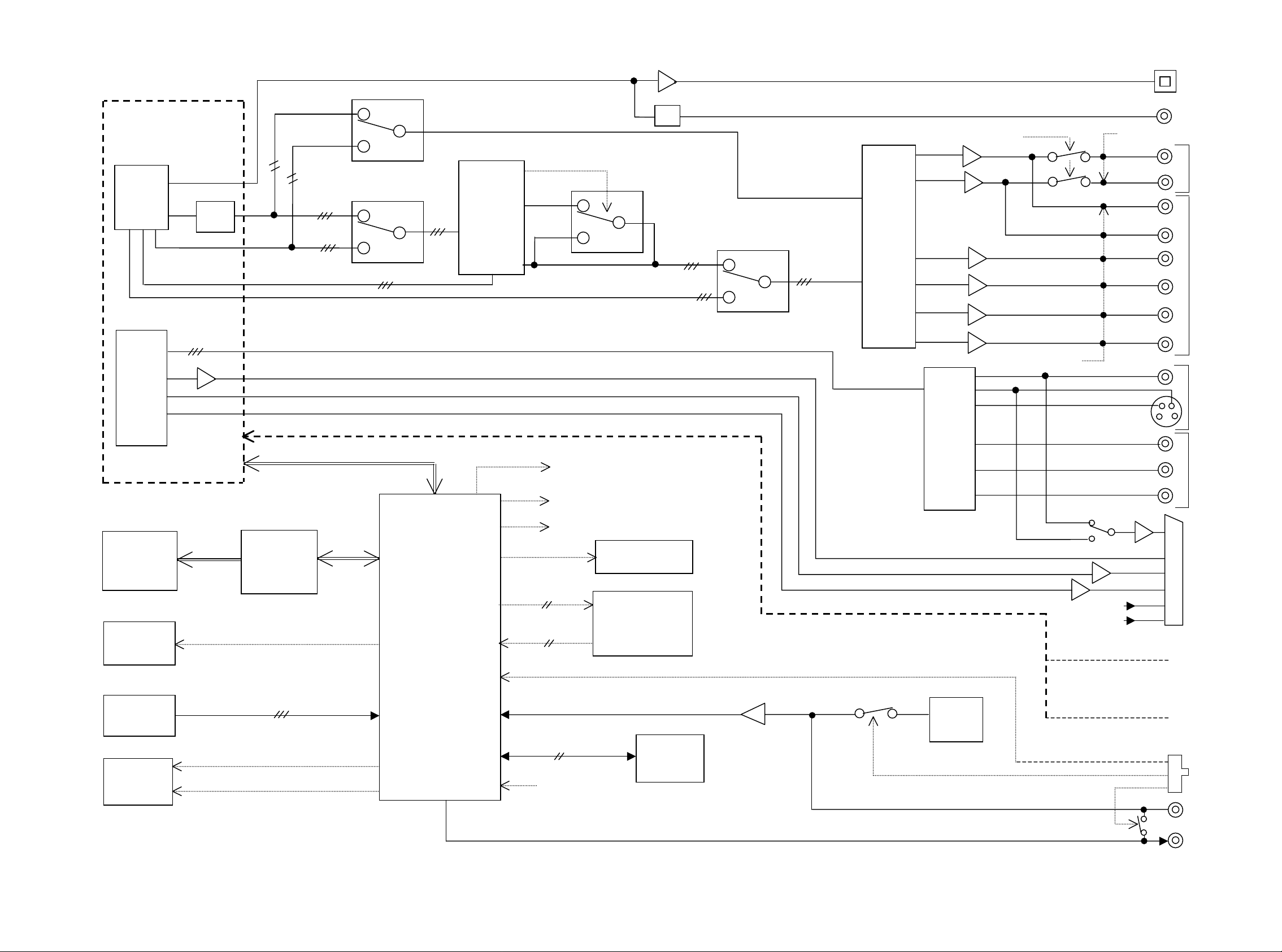
6. BLOCK DIAGRAM
DVD MODULE
AV
DEC
AC3/PCM
DIR
DIR
DIR_LRCK
DIR_BCK
AV_LRCK
AV_BCK
DIR_DA TA
DIR_LRCK
DIR_BCK
L/R(2CH) ,AV1_LRCK
AV1_BCK
Q441
DVD_DTS
Q551
DVD
CD
FL/FR , C/LFE LS/RS
Q501
DTS
DEC
DSP
2CH/6CH
2CH L/R
6CH L/R
Q502
DTS_L/R
DTS_LS/ RS
DTS_C/LFE
Q451
DTS
Q401
6CH
DAC
DVD/THROUGH
OPT
COAX
SYS_MUTE
SYS-L
SYS-R
L
R
LS
RS
J102
J101
J301
J201
Video
ENC
VF01
LCD
DISPLAY
DF02 - DF05
LCD
BL
SF01 - SF08
SF10,SF11
KEY
DF06
LED
Y , V/Cb
C/Cr
QF01
LCD
DRIVER
LCD_BL
KEY_IN_0 - 2
POWER_LED
STB_LED
QF02
FRONT
CPU
DVD/THROUGH
STB_MUTE
SYS_MUTE
POWER_ON
D_MOT OR_FWD
D_MOT OR_REV
DOOR_OPEN_SW
DOOR_CLOSE_SW
VERSION
I2C
SUPPLY
DOOR
MOTOR
BLOCK
L/R(2CH)
LS/RS
C/LFE
SYS_IN
QF05
EP-ROM
QF13,QF14
IR_SW
QV04
V-IF
IR
STB_MUTE
NTSC/PAL
VIDEO_SEL
SYS_SW
C
SW
C
Y
C
Cr
V
V/Y
R/C
B
G
L
R
JV02
JV03
C ONLY
J802
N ONLY
INT
EXT
SYSTEM
IN
SYS_OUT
OUT
7
8

7. WIRING DIAGRAM
DVD Mechanism Module
PC101
TLP910
12
CN201
SLDR MOTOR
(VNP1695)
CN203
43
FGSB
VWG2009
1
2FG3
CN202
V+5S
S_GND
M
SMEB
VWG2048
1
2
M
SPINDLE MOTOR
LIVE
NEUTRAL VKP2205
1INSIDE
8 INSIDE
2S_GND
7 S_GND
3SLDRF
6 SLDRF
4FG
5FG
5SLDR_R
4 SLDR_R
6V+5S
3 V+5S
7SPDL+
2 SPDL+
8SPDL-
1 SPDL-
CN302
LOMB
SPINDLE MOTOR
N1S ONLY
AC OUTLET
PS03
AC OUTLET
PCB
JP11
JP05
JP01
MSWB
1
2
PS02
MAIN
SWITCH PCB
PICK UP ASS’Y(OPU)
CN401
LOAD-
1 LOAD-
2
LOAD+
2 LOAD+
M
1
2
1
2
1
JP04
1
2
MPD-VR(650)
MPD-VR(780)
LOSB
VWG1885
CN303
CN106
FOR DOWNLOAD SOFTWARE
TO FLASH ROM
1/2SW
VREF(2.5V)
GND
VCC
MPD(650)
GND(650)
LD(650)
VSHF
MPD(780)
LD(780)
GND(780)
FOCSRTN
TRKGDRV
TRKGRTN
FOCSDRV
CN301
JP06
1
2
JF06
FOR DOWNLOAD SOFTWARE
TO uP
1
2
3
4
5
6
7
8
9
JF01
GND
CN602
1-12V
2AC1
3AC2
4POWERON
5EV+5V
6GNDD
7SSO
8SSI
9SSCK
SQUEEZE
VSEL_SW
-27V
P-MUTE
CN904
V_SEL
LETTER
GNDD
V/Cb/S
GNDD
C/Cr
NAPSW
SEL_IR
IR
V+5D
V+12D
XRESET
CN905
DTSBCLK
DTSLRCLK
DTSDATA
ADATA1
ADATA2
ADATA3
XCSDF2
XCSDF1
AUDRST
HIBITSEL
LAT_DAC
ADATA0
AODAI(AC3)
DAC_CLK
V_GND
V_GND
V_GND
VSEL2
Y
V+3V
6CHMD
LFEON
DFSI
DTSMD
44/X48
DFSO
DFSCK
XMUTE
BCK
LRCK
GNDD
GNDD
V+5V
V+12D
10XRESET
11LT1
12XRDY
13SEL_IR
14IR
15SW+5V
R/C
G
B
15
13
11
9
7
5
3
1
N1S ONLY
7
6
5
4
3
2
1
CN901
14
12
10
8
6
4
2
29
28
27
26
25
24
23
22
21
20
19
18
17
16
15
14
13
12
11
10
9
8
7
6
5
4
3
2
1
JV01
J601
CN120
1
A
2
B2
3
B1
4
5
6
B4
7
B3
8
C
9
10
RF
11
12
13
14
15
16
17
18
19
20
21
22
23
24
12SW2
11SW1(S_GND)
10SPDL9LOAD8SPDL+
7LOAD+
6SLDR_R
5V+5S
4SLDE_F
3FG
2INSIDE
1S_GND
1
A
2
B2
3
B1
4
1/2SW
5
VREF(2.5V)
6
B4
7
B3
8
C
9
GND
10
RF
11
VCC
12
MPD-VR(650)
13
MPD(650)
14
GND(650)
15
LD(650)
16
VSHF
17
MPD-VR(780)
18
MPD(780)
19
LD(780)
20
GND(780)
21
FOCSRTN
22
TRKGDRV
23
TRKGRTN
24
FOCSDRV
1 SW2
2 SW1(S_GND)
3 SPDL4 LOAD5 SPDL+
6 LOAD+
7 SLDR_R
8 V+5S
9 SLDE_F
10 FG
11 INSIDE
12 S_GND
DVDM
DVD MAIN PCB
(DIGITAL BOARD)
CN1030
CN106
1
TXD
2
RXD
3
DTR
4
CTS
5
V+5D
6
GNDD
7
N.C.
+3.3V
+3.3V
CN110
JP07
M+6V2M+6V
1
26
M+6V25M+6V
GNDM4GNDM
3
24
M-GND23M-GND
12V
5
22
SW+12V
12V
GND
6
7
21
20
GND
SW+12V
SUPB
GND9GND
8
19
GND18GND
SW+5V11SW+5V12SW+5V
10
17
16
SW+5V
SW+5V15SW+5V
+3.3V16+3.3V
GND18GND19GND20GND21GND
13
14
15
17
12
13
SW+3.4V
SW+3.4V
10
GND9GND8GND7GND6GND
SW+3.4V11SW+3.4V
14
PS01
POWER SUPPLY PCB
22
5
EV+5V
E+5V
POWERON
23
24
4
3
STB_CTL
AC2
M-REW
25
2
AC1
26
1
M-FWD
7
6
5
4
3
2
1
29
28
27
26
25
24
23
22
21
20
19
18
17
16
15
14
13
12
11
10
9
8
7
6
5
4
3
2
1
JV05
R/C
V-GND
G
V-GND
B
V-GND
VSEL2
VSEL1
15
SQUEEZE
14
LETTER
13
Y
12
V-GND
11
VIDEO/Cb
10
V-GND
9
C/Cr
8
NTSC/PAL
7
SEL-IR
6
IR
5
+5V
4
+12V
3
XRESET
2
VIDEO-SEL
1
+3.3V
DIRBCK
DIRLRCK
DIRDATA
6CH/2CHLFEON
LF.RF
C.LFE
LS.RS
DTSSD0
DTSMD
DTSXCSB
DTSXCS
XAUDRESET
CD/DVD
SDATA
SCLK
XRESET
XMUTE
DCXCO
AV1BCK
AV1LRCK
2CHDATA
AC3/PCM
D-GND
DACCLK
D-GND
+5V
+12V
1 P-MUTE
2 D-MOTOR-FWD
3 D-MOTOR-REW
4 POWER_ON
5 EV+5V
6 GND
7 S-OUT
8 S-IN
9 S-CLK
10 XRESET
11 LT
12 XREADY
13 D-CLOSE-SW
14 D-OPEN-SW
15 SW+5V
JF03
JF04
J104
1
1
JD01
/TRES
STB+5
TSUX3
TMODE
FROB
PF01
FRONT PCB
P-MUTE2SYS-MUT3STB-MUT4DVD/THR5SYS-IN6IR-SW7GND8SYS-SW9SYS-OUT
5
4
3
2
STB-MUT
SYS-MUT
SYS-IN
DVD/THR
P-MUTE
JCKB
PJ01
JACK PCB
DRIVE1
DRIVE2
-12V
3
4
1
-12V2DRIVE23DRIVE14M-GND
TCK
6
2
TEXD
7
IR-SW
M-GND
1
TTXD
8
GND
J105
TAUX
9
SYS-SW
10
GND
SYS-OUT
JF07
KEY_DOOR
GND
JF05
STB+5
GND
JF06
KEY_STBY
S-LED
P-LED
STB+5
GND
RC2
D-CLOSE
RC1
A-GND
A-GND
+12V
SQUEEZE
V-GND
V-GND
VSEL1
V-GND
V-GND
VSEL2
JV06
J106
DRIVE2
DRIVE1
M-GND
M-GND
D-OPEN
1
2
1
2
3
1
2
3
4
5
6
AR
AL
B
G
R/C
+8V
+5V
V
Y
JF08
1
KEY_DOOR
2
GND
JF12
1
STB+5
2
RC1
3
GND
N1S ONLY
19
18
17
16
15
14
13
12
11
10
9
8
7
6
5
4
3
2
1
1
2
3
4
5
6
PF02
DOOR
PCB
PF05
RC
CENTER
PCB
J801
1
2
3
4
5
6
7
8
9
10
11
12
13
14
15
16
17
18
19
6
5
4
3
2
1
PF04 RC LEFT PCB
JF09
1
KEY_STBY
2
S-LED
3
P-LED
4
STB+5
5
GND
6
RC2
AR
A-GND
AL
A-GND
B
+12V
SQUEEZE
V-GND
G
V-GND
R/C
+8V
VSEL1
+5V
V
V-GND
Y
V-GND
VSEL2
DRIVE2
DRIVE1
D-CLOSE
M-GND
M-GND
D-OPEN
1
STB+5
PF03
LED PCB
PC01
SCART PCB
SCRB
M
DOOR MOTOR
GND2RC23STB+5
GND2RC2
JF11
1
3
JF10
9
10

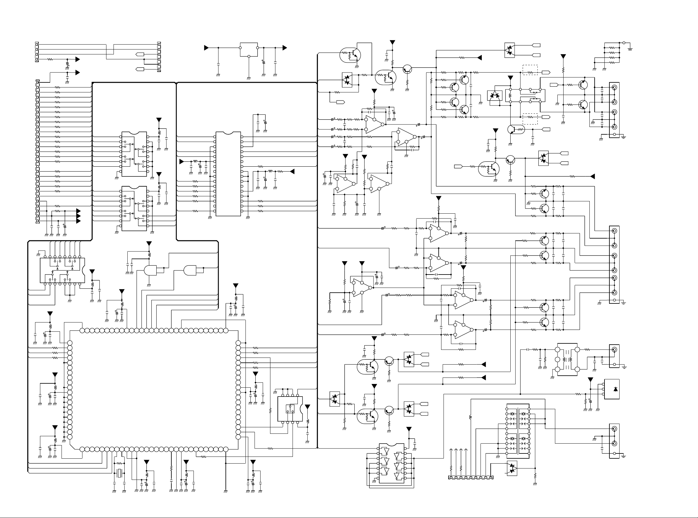
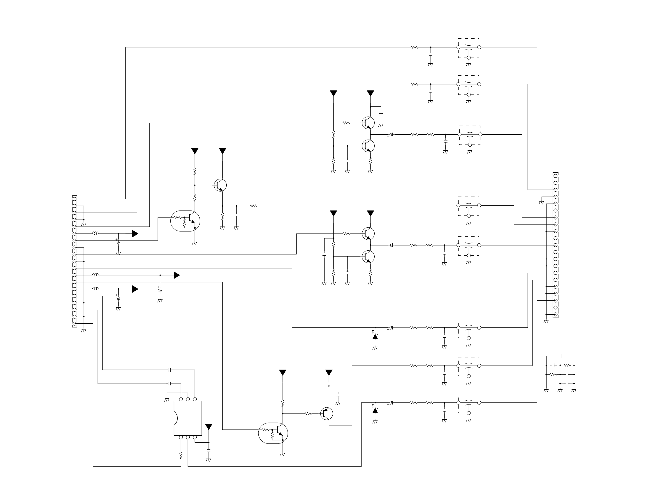
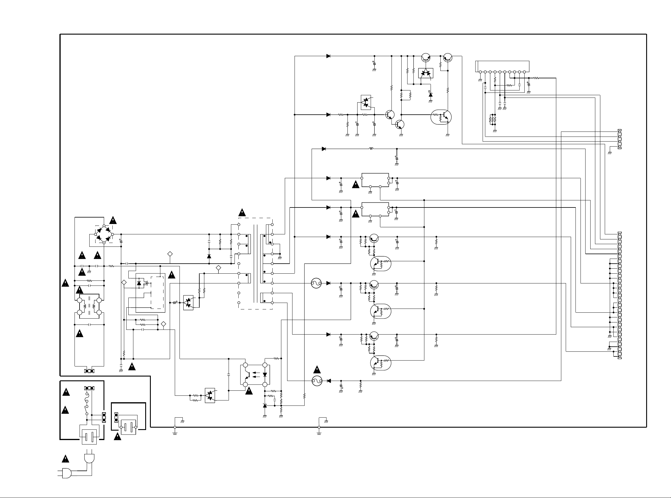
8. SCHEMATIC DIAGRAM AND PARTS LOCATION
PF01
WG404K1060
Download Connector
TMODE
TAUX3
4.9V
STB+5
FROM DVDM CN602
P-MUTE
D-MOTOR-FWD
D-MOTOR-REV
POWER_ON
EV+5V
GND
S-OUT
S-IN
S-CLK
XRESET
XREADY
D-CLOSE-SW
D-OPEN-SW
SW+5V
FROM PJ01 J104 4(K-11)
P-MUTE
SYS-MUT
STB-MUT
DVD/THR
SYS-IN
IR-SW
GND
SYS-SW
SYS-OUT
STB+5
/TRES
TRXD
TTXD
TAUX
LT
LCD+5
RF08
N.C.
N.C.
RF09
JF01
1
GND
4.9V
2
3
4
5
6
TCK
7
8
9
10
GND
GND
RF82
10K
RF83
10K
STB+5
LED+5
4.9V
100
100
RF58
RF57
RF56
DF02
NSCW100
DF04
DF03
NSCW100
NSCW100
QF10
DTC323TU
GND
JF03
1
2
3
4
5
6
7
8
9
10
11
12
13
14
15
GND
JF04
1
-14.1V
2
3
4
5
6
7
8
9
-13.5V
-14.4V
4.8V
CF04 47u/10V
4.9V
GNDGND
FF01
BLM11P600SPT
FF02
BLM11P600SPT
CF09
GND
CF05 0.1
47u/10V
GND
RF10 100
RF11 100
RF12 100
RF13 100
RF14 100
RF15 100
CF10
0.1
4.9V
4.9V
STB+5
LCD+5
LED+5
CF06 N.C.
CF07 N.C.
GND GND GND
CF08 N.C.
GND
LCD+5
QF03
N.C.
RF07
N.C.
N.C.
CF01
GNDGND
LCD+5
STB+5
4.9V
0.1
CF23
GND
100
100
RF55
DF05
NSCW100
RF54
3.1V
100
RF81
N.C.
0V
VF01
HLC7599-016600
1 2 3 4 5 6 7 8 9 10 11 12 13 14 15 16 17 18 19 20 21 22 23 2425 26 27 28 29 30 31 32 33 34 35 36 37 38 39 40 41 42 43 44 4546 47 48 49 50 51 52 53 54 55
SEG[0]
SEG[1]
SEG[2]
SEG[3]
SEG[4]
SEG[5]
SEG[6]
SEG[7]
SEG[8]
SEG[9]
SEG[10]
SEG[11]
SEG[12]
SEG[13]
SEG[14]
SEG[15]
SEG[16]
SEG[17]
SEG[18]
SEG[19]
SEG[20]
SEG[21]
SEG[22]
SEG[23]
SEG[24]
SEG[25]
SEG[26]
SEG[27]
SEG[28]
SEG[29]
SEG[30]
SEG[31]
SEG[32]
SEG[33]
SEG[34]
SEG[35]
SEG[36]
SEG[37]
SEG[38]
SEG[39]
SEG[40]
SEG[41]
SEG[42]
SEG[43]
SEG[44]
SEG[45]
SEG[46]
RF86
1K
STB+5
SEG[16]
CF18
SEG[17]
232425
SEG[46]
SEG[47]
STB+5
4.9V
RF87
1K
0.1
SEG[18]
515253545556575859606162636465666768697071A072
SEG[45]
SEG[19]
SEG[47]
01234
SF06
OPEN/CLOSE
5KQNAE
GND
4.9V
KEY0
KEY1
KEY2
REV
RF40
18k
RF39
56k
JF07
1
KEY_DOOR
2
GND
GND
JF06
1
KEY_STBY
2
S-LED
3
P-LED
4
STB+5
5
GND
RF38
6
RC2
0
GND
KEY_DOOR
GND
KEY_STBY
STB_LED
POWER_LED
STB+5
GND
JF08
1
2
GND
JF09
1
2
3
4
5
6
RC2
GND
RC LEFT
PF04
WG404K1090
SEG[20]
50
SEG[21]
49
SEG[22]
48
SEG[23]
47
SEG[24]
46
SEG[25]
45
SEG[26]
44
SEG[27]
43
SEG[28]
42
SEG[29]
41
SEG[30]
40
SEG[31]
39
SEG[32]
38
SEG[33]
37
SEG[34]
36
SEG[35]
35
SEG[36]
34
SEG[37]
33
SEG[38]
32
SEG[39]
31
SEG[40]
30
SEG[41]
29
SEG[42]
28
SEG[43]
27
SEG[44]
26
STB+5
STB+5
STB+5
4.9V
22k
RF50
4.9V
22k
RF47
4.9V
22k
RF43
RF48
RF49
56k
33k
5.1CHPAUSE
SF01
5KQNAE
SF02
5KQNAE
DOLBY V
SF03
SF07
GND
5KQNAE
GND
5KQNAE
GND
GND
SF04
5KQNAE
GND
RF45
10K
STOP
RF41
10K
SF05
SF08
5KQNAE
GND
5KQNAE
RF44
18k
FWD
TRAY
RF46
5.6k
RF42
5.6k
PLAY
GND
STB+5
4.9V
RF35
N.C.
RF34
N : N.C
C : 10K
RF33
0
N : 0Ω
RF32
C : 12K
GND
STB+5
4.9V
STB+5
RF18
N.C.
4.9V
RF21
RF22
GND
7WP8
VCC
ADRESS02ADRESS13ADRESS24GND
1
10k
RF19
10k
CF13
0.1
GND
100
RF20
100
5
6
SCL
SDA
CF11 N.C.
CF12 N.C.
GND GND
QF05
AT24C04
GND
STB+5
REVFWDPAUSE STOP
DOOR
OPEN/CLOSE
PF02
WG4704K1070
220
RF59
QF12
DTC114TE
3
GND
GND
QF13
RPM6936-V4
STBYTRAYDOORPLAY
DOLBY V5.1CH
SF10
5KQNAE12
GND
DOOR
180
RF60
DF06
SML-020MVT
QF11
DTC114TE
GND
2
1
JF10
RC2
STB+5
JF11
STB+52RC23GND
1
1
2
GND
PF03
WG404K1080
RF61
100
3
0.1
CF24
GND
GND
RF62
CF25
STBY
SF11
5KQNAE
100
10/16V
GND
LED
COM[0]
COM[1]
COM[2]
COM[3]
COM[4]
COM[5]
COM[6]
1M
RF80
LCD_/RD
LCD_/WR
74
75
76
COM[0]
COM[1]
COM[2]
COM[3]
COM[4]
COM[5]
COM[6]
GND
QF01
NJU6450A
77
78
79
80
81
82
83
84
85
86
87
88
89
90
91
92
93
94
95
96
97
98
99
100
D[0]
D[1]
D[2]
D[3]
D[4]
D[5]
D[6]
D[7]
470
GND
RF01
0.4V
1.3V
2.2V
3.1V
4.0V
4.9V
0.1
CF02
RST
1K
RF02
1K
RF03
1K
RF04
1K
RF05
RF88
N.C.
RF06
1k
CF03
47u/10V
GND GND
RF53 47K
1
OUT
CF19
4.9V
80
79
77
76
PA378PA2
2
1
8MHz
XF01
3
GND
RST
LCD_/WR
LCD_/RD
A0
D[0]
D[1]
0V
D[2]
D[3]
D[4]
D[5]
D[6]
D[7]
GND
QF09
DTC323TU
STB+5
DTA114EUA
81
Vss
GND
82
X0
83
X1
84
Vcc
85
P00/AD00
RF65 0
86
P01/AD01
87
P02/AD02
RF66 0
88
P03/AD03
RF67 0
89
P04/AD04
RF68 0
90
P05/AD05
RF69 0
91
P06/AD06
92
P07/AD07
93
P10/AD08
RF70 0
94
P11/AD09
RF71 0
95
P12/AD10
RF72 0
96
P13/AD11
RF73 0
97
P14/AD12
RF74 0
98
RF75 0
99
RF76 0
100
RF77 0
4.9V
QF02
MB90F553A
QF15
-13.5V
-RST
PA4/CKOT
PA1/OUT375PA0/OUT2
P15/AD13
P16/AD14
P17/AD15
P20/A162P21/A173P22/A184P23/A195P24/A206P25/A217P26/A228P27/A239030/ALE10P31/-RD11Vss12P32/-WRL13P33/-WRH14P34/HRQ15P35/-HAK16P36/RDY17P37/CLK18P40/SCK19P41/SOT20P42/SIN
1
4.9V
0.047
CF20
N.C.
GND
GND
74
P97/PPG573P96/PPG472P95/PPG371P94/PPG270P93/PPG169P92/PPG0
GND
STB+5
4.9V
QF16
DTA114EUA
2
68
4.9V
OSC173OSC2
VSS
VDD
/RST
FR
V5
V3
V2
M/S
V4
V1
COM72COM83COM94COM105COM116COM127COM138COM149COM1510SEG6011SEG5912SEG5813SEG5714SEG5615SEG5516SEG5417SEG5318SEG5219SEG5120SEG5021SEG4922SEG48
1
3
4.9V
IN
STB+5
GND
QF08
S-806D
GND
66
P87/IN365P86/IN264P85/IN163P84/IN0
P91/OUT167P90/OUT0
SEG[3]
SEG[2]
SEG[1]
SEG[0]
A0
62
60
58
P81/TIN159P80/TIN0
P77/IRQ757P76/IRQ656P75/IRQ555P74/IRQ454P73/IRQ353P72/IRQ2
P83/TOT161P82/TOT0
P43/SCK122P44/SOT123Vcc24P45/SIN125P46/ADTG26P47/SCK027C28P50/SDA0/SOT029P51/SCL0/SIN030P52/SDA1
21
CF14
GND
SEG[4]
4.9V
SEG[9]
SEG[8]
SEG[7]
SEG[6]
SEG[5]
SEG[10]
SEG[11]
SEG[12]
SEG[13]
SEG[14]
SEG[15]
STB+5
P55/SCL2
P54/SDA2
P53/SCL1
4.9V
RF52
52
51
-HST
10K
MD2
P71/IRQ1
P70/IRQ0
P67/AN7
P66/AN6
P65/AN5
P64/AN4
P63/AN3
P62/AN2
P61/AN1
P60/AN0
AVRL
AVRH
STB+5
4.9V
10K
RF51
GND
10K
RF37
50
MD1
49
MD0
RF36
48
10K
47
46
45
44
43
42
Vss
41
40
39
RF85
38
1K
37
AVss
36
4.9V
35
34
AVcc
33
32
31
GND
GND
0.1
CF15
GND
STB+5
0.1
STB+5
4.9V
STB+5
4.9V
RF23 10K
JF05
1
STB+5
RF31
2
RC1
3
0
STB+5
100
QF06
DTA114EUA
4.8V
RF28
N.C.
RF27
4.7K
DF01
1SS301
47K
RF25
GND
RF29
4.9V
4.9V
0.1
CF17
GND
QF07
2SA1586
4.8V
N.C.
CF28
GND
-2.6V
0
RF26
1
0.3V
GND
8
QF04
4
TC7W14FU(1/3)
0.1
CF16
7
4.9V
SF09
SSSS822101
654
N.C.
RF30
321
GND
RF78
RF17
330
2
0V
QF04
TC7W14FU(2/3)
RF84
N.C.
0
6
4.9V
1211
GND
GND
STB+5
JF12
GND
RC1
1
2
3
GND
QF14
RPM6936
PF05
WG404K1100
RC CENTER
1
GND
RF64
100
RF63
100
3
CF27
CF26
0.1
2
10/16V
GND
GND
FROM PS01 JD01 1(C-15) TO DOOR MOTOR
1
M-GND
2
DRIVE1
3
DRIVE2
-12V -12V
DIRBCK
DIRLRCK
DIRDATA
6CH/2CH-
LFEON
DTSSDO
DTSMD
DTSXCSB
DTSXCS
XAUDRESET
CD/DVD
SDATA
XRESET
XMUTE
DCXCD
AV1BCK
AV1LRCK
2CHDATA
AC3/PCM
D-GND
DACCLK
D-GND
FROM DVDM
CN905
J105
+3.3V
LF,RF
C,LFE
LS,RS
SCLK
+5V
+12V
D-GND
DTSDATA
L/R_FL/FR
DIRDATA
C530
0.1
DTSLRCK
DTSBCK
DTSDATA
FL/FR
LS/RS
C/LFE
J601
D-GND
C533
0.1
D-GND
0.1
C503
D-GND
4
29
28
27
26
25
24
23
22
21
20
19
18
17
16
15
14
13
12
11
10
9
8
7
6
5
4
3
2
1
D-GND
C529
D-GND
R116 0
D-GND
GND
3.4V
100/10V
C532
D-GND
C502
D-GND
V+3A
3.4V
100/10V
3.4V
100/10V
-13.7V
C604
100/16V
D-GND
3.4V
C601
0.1
D-GND
R601 0
R602 0
R603 0
R604 0
R605 0
R606 100
R607 100
R608 100
R609 0
R610 0
R611 0
R612 0
R613 0
R614 0
R615 0
R616 0
R617 0
R618 0
R619 100
R620 100
R621 100
R622 BLM11B601S
R623 0
4.8V
4.8V
11.0V
C602 0.1
C603 0.1
C605 N.C.
D-GND
D-GND
DTSBCK
AV1BCK
DIRLRCK
DTSLRCK
AV1LRCK
LHLH
LHLH
D-GND
F510
BLM11P600SPT
0.1
C528
D-GND
81
R519 0
82
R520 0
83
R521 0
84
85
86
V+3A
87
88
89
90
F511
BLM11P600SPT
91
92
0.1
C531
93
D-GND
94
95
96
97
V+3A
98
99
100
F501
BLM11P600SPT
D-GND
0.1
C501
Q501
YSS912C-F
D-GND
DIRBCK
14131211109
VDD2
SDWCK0
SDBCK0
SDIA0
SDIA1
RAMA1
RAMA0
RAMWEN
RAMDEN
VSS
VDD2
IPORT7
IPORT6
IPORT5
IPORT4
IPORT3
IPORT2
IPORT1
IPORT0
VSS
V+3A
DIRBCK
DIRLRCK
DIRDATA
6CH/2CH-
LFEON
FL/FR
C/LFE
LS/RS
DTSSD0
DTSMD
DTSXCSB
DTSMD
DTSXCS
AV1LRCK
AUDRST
DIRLRCK
CD/DVD-
DACLRCK
SDATA
AV1BCK
SCLK
DIRBCK
DACBCK
XMUTE
DACXCS
AV1BCK
AV1LRCK
L/R_FL/FR
XAVDM
AC3/PCM
L/R_FL/FR
DTS_L/R
DACCLK
DAC_L/R
C/LFE
V+5M
DTS_C/LFE
V+5A
DAC_C/LFE
V+12D
CD/DVD-
12345678
Q551
TC74VHC157FT
V+3A
3.4V
VCC15ST-
F551
16
BLM11P600SPT
0.1
C551
D-GND
D-GND
80
79
VSS
RAMD778RAMD677RAMD576RAMD475RAMD374RAMD273RAMD172RAMD0
VDD12RAMCEN3RAMA164RAMA55SD1806SD1817SD1828XI9XO10VSS11AVDD12SD18313TEST14TEST15DVFB16DTSDATA17AC3DATA18SD08319CPO20AVSS
1
C552
0.1
0.1
C527
X501
12.288MHz
D_CLOSE_SW
D_OPEN_SW
12345678
12345678
D-GND
D-GND
V+5A
4.8V
C526
100/10V
D-GNDD-GND
D-GND
R504
1M
C504
22p
D-GND D-GND
Q441
TC74VHC157FT
LLH
H
GND
Q451
TC74VHC157FT
HL
HL
GND
0.1
C524
D-GND
F509
BLM11P600SPT
0.1
C525
71
70
VDD1
22p
C505
D-GND D-GND
16
VCC
15
ST-
14131211109
HHLL
D-GNDD-GND
16
VCC
15
ST-
14131211109
L
LH
H
D-GND
V+5A
4.8V
8
0.1
C523
3
4
D-GND
69
68SI67SO66
SCK
RAMA2
V+3A
3.4V 3.4V
F502
BLM11P600SPT
C507
0.1
C506
D-GND
D-GND
D-GND
TC7W08FU(2/2)
/CS
100/10V
DRIVE2
6
DRIVE1
5
D-CLOSE
4
M-GND
3
M-GND
2
D-OPEN
1
J106
V+3A
F441
BLM11P600SPT
C442
0.1
C441
D-GND
D-GND
V+3A
F451
BLM11P600SPT
C452
0.1
C451
D-GND
D-GND
DTS_LS/RS
DAC_LS/RS
F508
BLM11P600SPT
5
6
Q503
65
64
/CSB
RAMA3
0.1
C508
13
3.4V
CENTER
0.1
WOOFER
LSUR
RSUR
BLM11P600SPT
V+3A
0.1
3.4V
C401
A-GND
DACBCK
3.4V
DACLRCK
DAC_L/R
0.1
DAC_C/LFE
DAC_LS/RS
DACCLK
LS/RS
7
Q503
TC7W08FU(1/2)
63
62
61
60
59
/IC
VSS
TEST
RAMA4
RAMA558RAMA6
VDD222SDOA223SDOA124SDOA025RAMA1426RAMA1327RAMA1228RAMA1129RAMA1030VSS
21
V+3A
10k
R505
F503
BLM11P600SPT
C509
470p
D-GND
C510 0.1
D-GND
D-GND
C511
100/10V
D-GND
F401
C402
A-GND
R401 0
R402 0
R403 0
R404 0
R405 0
R406
0
57
11.0V
V+12D
0.1
C391
A-GND A-GND A-GND
1
OUT3
2
OUT4
3
VSSA
4
OUT5
5
OUT5
6
VDOA
7
N.C.
0.1
C403
8
1
2
56
R506
0.1
A-GND
DTSXCS
DTSXCSB
AUDRST
55
SURENC
KARAOKE
0
A-GND
SCLK
SDATA
DTSSD0
54
MUTE
N.C.
9
STATIC/L3-
10
BCK
11
LRCK
12
DATA12
13
DATA34
14
DATA56
15
N.C.
16
SYSCLK
53
52
CRC
100/10V
/SDBCK0
C512
Q401
UDA1328T/S1
F507
0.1
C520
D-GND
51
VDD2
VSS
NONPCM
SDWCK1
SDBCK1
SDOB0
SDOB1
SDOB2
RAMA7
TAMA8
TAMA9
VDD2
VSS
DPORT7
DPORT6
DPORT5
DPORT4
DPORT3
DOPRT2
DOPRT1
DPORT0
VDD1
D-GND
A-GND
OUT2
OUT2-
VREF
OUT1-
OUT1
TEST1
DS
DEEM0
DEEM1
MUTE
TEST2
VDDD
VSSD
SDATA
SCLK
XCS
V+3A
3.4V
BLM11P600SPT
C521
D-GND
50
49
48
47
46
45
44
43
42
41
40
39
38
37
36
35
34
33
32
31
Q391
uPC29M10HB
2
32
31
30
29
28
27
26
25
24
23
22
21
20
19
18
17
D-GND
0.1
C522
100/10V
D-GND
R512
R511 0
R509 0
R508 0
F506
C517 0.1
D-GND
V+5A
F504
BLM11P600SPT
0.1
C513
D-GND D-GND
8.9V
31
0.1
C408
A-GNDA-GND
R411
0
BLM11P600SPT
0.1
C406
D-GND
D-GND
R409 0
R408 0
R407 0
0
V+3A
3.4V
BLM11P600SPT
C519
C518
100/10V
D-GNDD-GND
R507
4.8V
0.1
C515
C514
100/10V
D-GND
C394
C407
F402
C405
0.1
0
220/16V
100/10V
100/10V
D-GND
D-GND
R510
0
V+12A
0.1
C395
3.4V
R410
0
0.1
C404
4
VSS
H
YSS6CH6CH17CH08VD1
5
6CH/2CH-
DS
3.4V
XMUTE
4.8V
C303
LEFT-
100/16V
C301
LEFT
100/16V
RIGHT
RIGHT
C302
RIGHT-
100/16V
RIGHT-
LEFT
DS
SCLK
F505
BLM11P600SPT
0.1
C516
100/16V
WOOFER
LFEON
3.3V
XMUTE
AC3/PCM
C314
A-GNDA-GND
R288
C304
100/16V
C317
47K
D231
1SS301
VEE
LEFT-
V+3A
SDATA
DACXCS
CENTER
LSUR
RSUR
AV1LRCK
AV1BCK
DTS_LS/RS
DTS_C/LFE
DTS_L/R
1
2
3
Q502
TC7W53FU
INH
V+5A
COMMON
L
4.8V
D-GND
XAVDM
PJ01
WG404K1010
V:PLAY COLOR BAR (PAL),1kHz
DTC124EUA
0V
D351
1SS301
R363
1k
R303
22k
R301
22k
R302
22k
R304
22k
V+12A
8.9V
0
R315
C313
0.1
6
-
+
5
NJM2068(1/2)
R395
47K
0.1
A-GNDA-GND A-GNDA-GND
V+12A V+12A
8.9V
R221
47K
C221
47/16V
A-GND A-GNDA-GND
Q360
XMUTE
R307
22k
C305
R305
22k
C306
8
Q302
2.0V
R233
10k
R235
A-GND
68p
R333
2.2K
R306
22k
68p
R308
22k
47k
R313
7
2
3
C222
A-GND
DTC124EUA
4.8V
10k
R364
3.9V
R309 47k
C307
R331
2.2K
V+12A
C311
R316
R317
C316
8.9V
-
+
0.1
A-GND
C265
0.1
Q283
C225
0.1
A-GND
Q233
DTC124EUA
1k
3.7V
8.9V
33p
6
-
5
+
R332 2.2K
R334 2.2K
33p
8.9V
NJM2068(2/2)
0
2
47k
3
C315
47/16V
8
1
Q221
NJM2068
4
V+5M
V+5M
A-GND
DTC124EUA
V+12A
0
R311
8
Q301
NJM2114M(1/2)
Q302
-
+4
0.1
A-GND
C251
100/16V
C223
47/16V
A-GND
C202
100/16V
4.8V
2.2K
R286
0.2V
A-GND
4.8V
1K
R236
0.07V
A-GNDA-GND
1234567
D-GND
V+5M
C357
0.1
Q355
A-GND A-GND
C309
0.1
A-GND A-GND
7
R314 47k
1
R265
2.2K
0.1
C224
100/16V
A-GND
C201
100/16V
R267
2.2K
Q284
2SA1576A
0V
R287
A-GND
Q234
2SA1576A
0V
R237
A-GND
Q111
TC74HCU04
4.8V
C312
C252
10k
-13.0V
10k
R365
0.1V
3
2
R266
2.2K
1.2K
2SA1576A
C310
47/16V
Q301
NJM2114M(2/2)
+
-4
A-GND
33p
R251
15k
R252
820
R202
15k
1SS301
-13.0V
D232
1SS301
Q356
R201
D282
V+5A
15k
0V
141312111098
R366
100/16V
R310
47k
C308
4.8V
D-GND
4.7k
33p
R254
2.2k
-13.1V
C319
C320
1
100/16V
R253
10k
C253
220p
A-GND
-14.5V
-14.1V
-14.5V
-14.1V
C111
0.01
FROM PF01
JF04 2(G-1)
R351 100kR352 100k
R362
2.2K
R255
33k
C255
33p
2
-
+
3
NJM2068(1/2)
5
+
-
6
NJM2068(2/2)
C256 0.047
R256
6.8k
A-GND
STB_MUTE
P_MUTE
STB_MUTE
P_MUTE
R353
150
R361
2.2K
R359
2.2K
Q351
2SC4213
Q352
2SC4213
R360
2.2K
R354
150
V+12A
8.9V
R263
8
Q251
4
Q251
R203
R204
Q354
2SC4213
XMUTE
0
1
10k
C203
C204
10K
J104
7
220p
220p
R392
470K
R355
150
R356
150
4.8V
C257
A-GND
10/50V
C260
100/16V
8.9V
R205 33k
C205
33p
2
-
+
3
NJM2068(1/2)
5
+
-
6
NJM2068(2/2)
C206 33p
R206
33k
R289
470K
R290
470K
SYS_MUTE
P_MUTE
-14.1V
-14.5V
-13.5V
R1140R115
1
2
P-MUTE
SYS-MUT3STB-MUT
-13.7V
0.1
C259
R257
R258
V+12A
R213
0
8
Q201
4
Q201
F111
BLM11B601S
STB_MUTE
DVD/THROUGH
4.8V
0
4
DVD/THR
R325
5
R358
0
100k
100k
1
7
-13.7V
-13.7V
SYS-IN
R357
0
Q353
2SC4213
C351
100p
C352
100p
0
A-GND
6
IR-SW
-12V
D353
1SS301
A-GND
A-GND
Q305
DTC124EUA
0.1
C207
C209
10/50V
C210
10/50V
7
8
GND
SYS-SW
2
31
0.01V
Q359
DTC323TU
V+5M
4.8V
0.1
C326
R326
0.1V
A-GND
100k
R207
100k
R208
-12V-12V
D-GND
0V
9
SYS-OUT
14
1SS301
D352
V+12A
8.9V
87
+
-
12
A-GND
1K
Q306
2SA1576A
0.05V
R327
4.7k
A-GND
S131 SSSF141700
1112131415
1617181920
31
1SS301
D110
N1S
R369
0
L351
MR62-12USR
34
N1S
R370
0
-13.0V
A-GND
R281
2.2K
R282
1K
R231
2.2K
R232
2.2K
C112
0.1
0.3V
2
D-GND
-14.5V
-14.1V
56
4.8V
0.1
C359
A-GND
D302
1SS301
R319
150
R323
2.2K
R324
2.2K
R320
150
R259
150
R260
150
R209
150
R210
150
R111
100
47p
C113
D-GND
12345
109876
R117
47k
STB_MUTE
P_MUTE
AL
SYS_MUTE
-13.5V
A-GND
AR
DVD/THROUGH
Q303
2SC4213
Q304
2SC4213
Q281
2SC4213
Q282
2SC4213
Q231
2SC4213
Q232
2SC4213
NC
2
R112
D-GND
1
D-GND
-12V
-13.7V
R393
100K
R367
2.2K
R368
2.2K
C325
N.C.
A-GND
-14.5V
STB_MUTE
-14.1V
P_MUTE
R394
470K
R321
150
C321
NC
C323
100p
100p
C324
C322
NC
R322
150
R261
150
C261NCC263
100p
NC
C262
C264
100p
R262
150
R211
150
C211NCC213
100p
NC
C212
C214
100p
R212
150
L111
TPS247MN-0386AN
Q357
2SC4213
Q358
2SC4213
-13.7V
43
6
R121
220
A-GND
R113
75
4.8V
R122
NC
J302
GND TERMINAL
1
R399 0
R398 0
R397 0
R396 0
A-GND
D-GND
C355
N.C
C356
C353
N.C
C354
N.C
A-GND
-12V
1
3
2
7
9
8
4
6
5
10
A-GND
1
2
3
C115
C114
4700p
0.022
D-GND
V+5A
321
GP1F32T
GND
VCC
INPUT
C121
47/16V
D-GND
D-GNDD-GND
1
3
D-GND
2
0.1
C133
4
J301
YKC21-3215
1
3
N.C
2
4
6
5
7
J201
YKC21-3324
J101
YKC21-3182
J102
D-BUS
J103
YKC21-3046
EARTH
IN_L
IN_R
OUT_L
OUT_R
FRONT
LEFT
FRONT
RIGHT
CENTER
SUB
WOOFER
LEFT
SURROUND
RIGHT
SURROUND
DIGITAL
OUT
GP1F32T
OPT OUT
IN
OUT

V+12V
FROM DVDM CN901
JV01
VSEL1
SQUEEZE
LETTER
V-GND
VIDEO/Cb
V-GND
NTSC/PAL
SEL-IR
XRESET
VIDEO-SEL
15
14
13
12
Y
11
10
9
8
C/Cr
7
6
5
IR
4
+5V
3
+12V
2
1
CV01
V-GND V-GND V-GND
RV04 220
RV05 220
4.9V
10/50V
TO PC01 J801 5(D-1)
JV06
19
AR
AL
+12V
R/C
+8V
+5V
18
17
16
15
B
14
13
12
11
G
10
9
8
7
6
5
V
4
3
Y
2
1
A-GND
A-GND
SQUEEZE
V-GND
V-GND
VSEL1
V-GND
V-GND
VSEL2
FROM DVDM CN904
7
R/C
G
B
JV05
6
5
4
3
2
1
V-GND
V-GND
V-GND
V-GND
VSEL2
11.0V
CV02
10/50V
11.0V
4.9V
A-GNDV-GND
N1S ONLY
PJ01
WG404K1010
D_CLOSE_SW
D_OPEN_SW
V+5V
+12V
AR
AL
+12V
V+5V
2.9V
RV34
V-GND
10k
CV32
V-GND
V+5V
4.9V
V-GND
4.9V
0.1
CV30 100p
RV33
CV31
V+5V
6.8k
100p
SV01
SSSF114800
33k
RV30
54321
V+5V
4.9V
RV31 10k
V-GNDV-GND
SV02
SSSF12-S06N0
1
2
3
V-GND
C1S ONLY
RV06
0
CV09
0.1
V-GND
RV32
8.2k
Y,C,COMPOSITE
Y,Cb,Cr
C1S ONLY
RV07
V-GND
0
N1S ONLY
RV38
4.7
8.4V
QV05
2SA1162
QV02
N.C
RV01
N.C
CV07 0.1
CV08 0.1
11.0V
RV39
N.C
CV12
100/16V
+12V
11.0V
RV42 0
N.C
RV02
QV01
N.C
N.C
CV03
V-GND V-GND
V+12V
11.0V
0.1CV11
CV10
100/16V
V-GNDV-GND
10.2V
RV40 N.C
RV41 0
0.1
V-GND
CV13
V-GNDV-GND
13
CV04 N.C
N.C
RV03
V-GND V-GND
V-GND
GND TERMINAL (N.C.)
V-GND
1
2
3
4
5
6
7
8
9
10
11
12
V-GND
RV37
0
QV03
N.C
2
CV05 N.C
V-GND
N1S ONLY
JV07
QV04
LA7138M
MUTE
TYPE_SEL
V_OUT
V,Cb_IN
YCMIX
SQUEEZE
Cb_OUT
LETTER
C,Cr_IN
C_OUT
GND
REG_OUT
Cr_OUT
VCC
C_DCOUT
Y_IN
Y_OUT2
AMP_SEL
DAC_DCOUT
Y_OUT1
RV24
0
RV25
0
CV15 0.1
V-GND V-GND
24
GND
23
22
21
20
VCC
19
18
GND
17
16
15
14
GND
13
V-GND
LV01
15
11.0V
0.1
CV06
V+12V
CV14
100/16V
RV51
47
1.2V
RV53 6.8K
820
RV55
V-GND
11.0V
V-GND
CV43
0.1
RV12
10k
QV06
V-GND
CV20
HN1C01F(1/2)
CV41
V-GND
QV06
HN1C01F(2/2)
47
RV57
RV54 6.8K
RV52
47
1.2V
820
RV56
0.1
V-GND
CV22
470/10V
CV24
470/10V
CV26
470/10V
0.1
470/10V
V+12V
QV07
11.0V
HN1C01F(1/2)
CV44
0.1
V-GND V-GND
RV13
33
RV16
RV15
33
33
RV18
RV17
33
33
RV21
RV20
33
33
RV0833RV09
CV16
CV42
V-GND
CV18 470/10V
QV07
HN1C01F(2/2)
47
RV58
RV14
33
V-GND
V-GND
N.C.
RV19
V-GND
V-GND
N.C.
RV22
V-GND
V-GND
FV01 NFM40R01C221
33
0.1
RV11
RV10
33
33
N.C.
CV21
N.C.
CV23
N.C
CV25
FV06 NFM41R01C221
N.C
CV27
12
N.C.
CV17
V-GND
12
N.C
CV19
V-GND
FV03 NFM41R01C221
12
3
V-GND
FV04 NFM41R01C221
12
3
V-GND
FV05 NFM41R01C221
12
3
V-GND
12
3
V-GND
7
3
V-GND
FV02 NFM41R01C221
3
4
V-GND
V-GND
V-GND
0
RV23
V-GND
2
V-GND
JV02
8
V-GND
JV02
V-GND
JV03
5
3
2
4
1
JV04
COMPOSITE
VIDEO
OUTPUT
(YELLOW)
6
3
S VIDEO
1
OUTPUT
5
ANALOG
COMPONENT
VIDEO
PUTOUT
Y(GREEN)
Cb(BLUE)
Cr(RED)
C1S ONLY
EARTH
15 16
R950
220
F950 NFM41R01C221
12
PC01
WG404K1020
FROM PJ01 JV06 3(E-1)
J801
1
AR
AL
+12V
R/C
+8V
+5V
2
3
4
A-GND
5
B
G
V
Y
6
7
8
9
10
11
12
13
14
15
16
17
18
19
V-GND
L801 15
L802 15
L803 15
A-GND
A-GND
SQUEEZE
V-GND
V-GND
VSEL1
V-GND
V-GND
VSEL2
11.0V
V-GND
4.8V
V-GND
C801
C805
47/16V
47/10V
VV+12V
V+5V
0V
4.8V
C803
V-GND
C821 0.1
C822 0.1
V-GND
Q812
MM1507XN
Q804
DTC114EUA
2
47/10V
654
11.0V
V+5VA
VV+12V
1
3
V-GND
4.7K
R808
R809
4.7k
V+5V
2
VV+12V
11.0V
1
3
10.4V
V-GND
Q803
2SC4116
56k
R816
V-GND
C812
0.01V
0.1
R812
470
390
A-GND
R951
220
V+5VA V+5VA
C951
390 C950
4.8V
R801
100
R802
3.9K
R803
1.5k
C808
V-GND
V-GND
V+5VA
4.8V 4.8V
R818
3.9K
C813
0.1
V-GND
V-GND
V+5VA
10K
R827
1.2k
R828
4.8V
2
1
V+5VA
4.8V
3
2
V-GND
Q809
2SA1586
1
4.8V
R819
1.5k
R817
100
V-GND
C819
0.1
Q806
2SC4116 1
C814
Q801
2SC4116
2
2
0.1
2
2
0.1
4.8V
V+5VA
V-GND
C-GND
C-GND
1
V-GND
3
1
Q802
2sc4116
3
R804
V-GND
3
1
Q807
2SC4116
3
R820
47
47
12
12
D802
5.6V
D803
5.6V
C807
0.1
C809
100/10V
C815
100/10V
C817
100/10V
C824
470/10V
21
A-GND
R805
R806
39
33
R821
R822
39
33
R82339R824
33
R832
R831
33
39
R834
R835
39
33
V-GND
V-GND
V-GND
V-GND
V-GND
3
A-GND
F951 NFM41R01C221
12
3
A-GND
F801 NFM41R01C221
12
C810
N.C
3
V-GND
F802 NFM41R01C221
12
3
V-GND
F803 NFM41R01C221
12
C816
N.C.
3
V-GND
F804 NFM41R01C221
12
C818
N.C.
3
V-GND
F805 NFM41R01C221
12
C820
N.C.
3
V-GND
F806 NFM41R01C221
12
C825
N.C.
3
V-GND
J802
SCART CONNECTOR
1
R_OUT
2
R_IN
3
L_OUT
4
A-GND
5
10
11
12
13
14
15
16
17
18
19
20
21
V-GND
V-GND
6
L_IN
7
B
8
SQUEEZE
9
V-GND
N.C.
G
N.C.
V-GND
V-GND
R/C
BLANK
V-GND
V-GND
V/Y_OUT
V_IN
V-GND
C828
0.1
C952
0.1
R952
0
C-GNDA-GND V-GND
R836
0
C826
0.1
C827
N.C.
A-GND
N1S only
V:PLAY COLOR BAR (PAL),1kHz
3.3V
123
0
R833
4.8V
V-GND
C823
0.1
Q808
DTC114EUA
3
V-GND
1817
CP03
220p/250v
4
FP01
T1.25AL 250V
SP01
ESB92S94B
MAIN SWITCH
PS02
WG404K1040
34
CP04
220p/250v
GND
RP01 1M 1W
CP02
ECQUN
0.1/250v
LP02
CP01
0.1/250v
1
2
JP06
1
2
JP04
JP03
JP02
21
BROWN
JP01
YKE31-0129
1
23
JP05
2
1
BLUE
1
2
82k 2W
RP02
N1S ONLY
2
1
DP01
S1WB(A)60
CP08
150p 2KV
4
CP10
GND
AC OUTLET
PS03
JP11
WG404K1050
2
AC OUTLET
CP05
120/400V
RP11
0.47 1W
220p/250V
1
D
2
S
5
O.C.P/F.B
3
GND
CP09
470p
1
JP10
2S-770T-210
QP01
STR-G6551
RP09
1.2K
RP10
1.2K
1
4
Vin
CP11
100/50V
OSC
3
JP08
EARTH
DP04
1SS301
GND
RP18
6.8k
RP19
6.8k
RP14
QD01
QP15
2SC4116
6.7V
10kRP44
5.5V
22k
22k
RP42
GND
DTC114EU
4.8V
CP26
GNDGND
0.1/50V
DTC114EU
RP32
4.7k
DTC114EU
GND
RP39
3.3M
LP03 15uH
QP07 SI3033C
5
QP08
SI-3050C
5
4.7k
4.7k
RP28
RP29
RP51
0.03V
QP10
4.7k
RP33
RP34
0.03V
QP12
DTC114EU
4.7k
RP47
RP48
RP53
0.03V
QP19
RP57
11.4V
CP25
GND
DP15
1SS301
2SC4116
CP27
10/16v
12
GND
12
GND
QP09
2SB1185
10.4V
RP52
4.7K
4.7K
GND
QP11
2SB1185
5.4V
1.8K
RP35
1.8K
M-GND
QP18
2SB1185
4.7k
11.8V
RP54
4.7K
4.7K
GND
10K
2200/16v
QP13
0.6V
3
4
3
4
CP22
CP30
47k
RP40
GND
GND
4.9V
GND
11.1V
2200/16V
GND
6.0V
M-GND
12.5V
1000/16V
GND
GNDGND
CP20
CP24
10k
RP41
0.02V
CP16
470/10V
CP18
220/10V
220/10V
220/16V
RP43
QP14
2SC4116
DP13
SFPL52
PS01
WG404K1030
RP37
DP14
SFPL52 1k
10.3V
4.9V
DP08
U1BC44
DP09
RK46
DP10
FP06
T800mA 250V
FP07
T250mA 250V
JP09
EARTH
RK46
DP11
EK19
DP12
RK46
DP20
EK19
DP18
SFPL52
GND
TP01
1
2
3
RP08
RP07
CP06
0.047
0
RP15
N.C.
DP07
1SS301
82K 2W
DP02
ERA22-10
2
CP13
CP07
N.C
82K 2W
N.C
4
5
6
7
8
9
QP03
PC123F2
4
3
QP04
TL431
4.1V
RP24
0
GND
5.2V
18
17
16
15
GND
14
13
12
11
10
RP21
820
1
2
RP23
N.C.
RP25
2.7k
RP30
15k
RP26
1.5k
CP14
0.22
4.1V
RP27
2.2k
GND
9.7V 1.2V
22k
RP38
4.5V 3.3V
CP17
1000/10v
GND
5.7V
CP19
1000/10v
GND
11.1V
CP21
1000/16v
GND
6.1V
CP23
1000/10v
M-GND
12.5V
CP29
1000/16v
GND
-13.8V
CP28
220/25V
GND
RP45
QP17
7.5V
47k
DP16
1SS301
DP17
GND
M-GND
GND
2SA1586
5.8V
MA8056L 5.6V
6.2V
GND
10k
RP31
10k
RP36
10k
RP50
QP16
-13.6V
RP46
10k
QD01
LB1641
GND2DRIVE30.7V4VREF5CONT+6CONT-7VCC8VCC90.7V10DRIVE
1
GND
CD01
0.1
CD02
0.01
RD05
NC
RD06
GND
RD01
GND GND
NC
RD04
RD03
CD04
0.01
4.7 1/2W
CD05
220/16V
GND
RD02
220
2.7k
CD03
0.01
430
PIN NO.
1 0V
2 0.5V
3 0.7V
4 1.7V
5 0V
6 0V
7 12.4V
8 12.4V
9 0.7V
10 0.5V
M-GND
GND
M-GND
TO PJ01
J105 4(A-1)
JD01
1
-12V
2
DRIVE2
3
DRIVE1
4
M_GND
TO DVDM CN110
JP07
1
P-MUTE
2
M-FWD
3
M-REW
4
STB_CTL
5
E+5V
6
GND
7
GND
8
GND
9
GND
10
GND
11
SW+3.4V
12
SW+3.4V
13
SW+3.4V
14
SW+3.4V
15
SW+5V
16
SW+5V
17
SW+5V
18
GND
19
GND
20
SW+12V
21
GND
22
SW+12V
23
M-GND
24
M-GND
25
M+6V
26
M+6V
W001
19 20

PJ01
QF04 QF07 QF05 QF16 QF15 QF02 QF08 QF03 QF10 QF09
PF01
QV01QV02 Q284
QV05QV03 QV04 QV06 Q391 Q282 Q281
QF06
Q283
Q251
Q234
Q232
Q233
Q231
Q201
Q360
Q355
Q356 Q302
Q306
Q305
Q304
Q303
Q352
Q358
Q354
Q357
Q353
Q359
Q301
Q351
Q401
Q111
Q551
Q441
Q451 Q501
Q503 Q502
2221

QP08
QP07 QP10 QP09
PS01
QP12
QP11
QP19
QP16
QP18
QP14 QP04
QP15
QP17 QP13 QP03 QP01 QD01
PC01
N1S ONLY
Q802
Q801
Q803
Q804
Q807
Q806
Q809
Q808 Q812
PF02
QF11 QF12
PF03
PS02
PF04
QF13
PS03 N1S ONLY
QF14
PF05
2423

9. SERVICE MODE
10. WAVEFORM
Power requirements (Refer the circuitdiagram page 19 and 20)
Press<POWER>while pressing
<PLAY>and<PAUSE>
“SERVICE_1” is displayed
Pres s <FORWARD >
STANDBY LED Light on RED
Pres s <FORWARD >
“STB_LED” is displayed
MS code is displayed
MSO 2
Pres s <FORWARD >
Press<FORWARD >
STANDBY LED Light on GREEN
“POWER_L ED” is d i s p l ayed
Produc t v er s ion is d i s p l ayed
EURO 2
Pres s <FORWARD >
DV2100/N1S-----EURO 2
DV2100/C1S ----- ASIA 3
All p art s o f L CD is t u r n ed on
1
2
100V 10usec
10V 10usec
0.1V 10usec
3
4
50mV 10usec
Press<FORWARD >
Pres s <FORWARD >
Each Segment is displaye d on e by one
Pres s <FORWARD >
Chec k o f k ey
When key i s d ep r e ssed ,k ey n ame is d i s pl ay ed
Pr es s <PL AY>and <PAUSE>
Cance li ng th e Serv i ce Mod e
The Service Mode is canceled by turning the power off.
Vers ion o f
“VER
Front
-COM is displayed
” is displayed
25
26

11. REMOVE THE DVD MECHANISM
Taking the disk out for EMERGENCY. (For example: when it is not possible
to turn on the product. The disc can not be taken out from the loader.)
1. Remove the front left leg. (See Fig. 1)
2. The hole is visible under the leg. (See Fig. 2)
3. Insert a screwdriver (minus) into the hole.
4. Move a screwdriver from rear to front, and turn the gear pulley in the hole. (See Fig. 3)
5. then the tray is moved a little. Pull the tray with your hand at this time.
Bottom of DV2100
Removed this leg.
Front panel
Fig. 1
Move the screwdriver this way.
Gear pulley
Fig. 2 Fig. 3
27
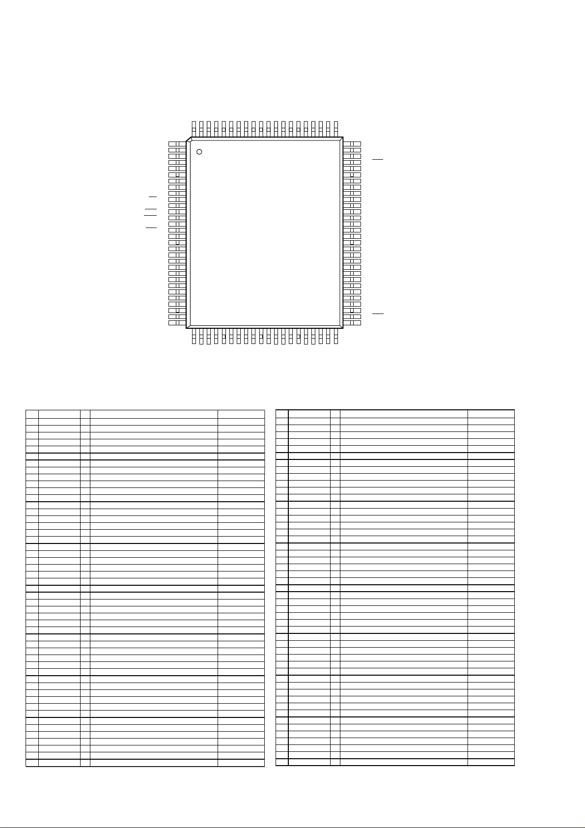
D
12. IC DATA
QF02 : MB9055A
PIN CONFIGURATION
P20/A16
P21/A17
P22/A18
P23/A19
P24/A20
P25/A21
P26/A22
P27/A23
P30/ALE
P31/RD
V
P32/WRL
P33/WRH
P34/HRQ
P35/HAK
P36/RDY
P37/CLK
P40/SCK
P41/SOT
P42/SIN
P43/SCK1
P44/SOT1
V
P45/SIN1
P46/ADTG
P47/SCK0
P50/SDA0/SOT0
P51/SCL0/SIN0
P52/SDA1
P17/AD15
P16/AD14
P15/AD13
P14/AD12
P13/AD11
P12/AD10
P11/AD09
P10/AD08
P07/AD07
P06/AD06
P05/AD05
P04/AD04
P03/AD03
P02/AD02
P01/AD01
P64/AN4
P65/AN5
P00/AD00
P66/AN6
P67/AN7
99989796959493929190898887868584838281
100
1
2
3
4
5
6
7
8
9
10
11
SS
12
13
14
15
16
17
18
19
20
21
22
CC
23
24
25
26
C
27
28
29
30
31323334353637383940414243444546474849
P53/SCL1
P55/SCL2
P54/SDA2
CC
AV
AVRL
AVRH
SS
AV
P60/AN0
P61/AN1
P62/AN2
P63/AN3
SS
V
VCCX1X0V
MD0
P70/IRQ0
P71/IRQ1
SS
50
MD1
80
79
78
77
76
75
74
73
72
71
70
69
68
67
66
65
64
63
62
61
60
59
58
57
56
55
54
53
52
51
PA4/CKOT
PA3
PA2
RST
PA1/OUT3
PA0/OUT2
P97/PPG5
P96/PPG4
P95/PPG3
P94/PPG2
P93/PPG1
P92/PPG0
P91/OUT1
P92/OUT0
P87/IN3
P86/IN2
P85/IN1
P84/IN0
P83/TOT1
P82/TOT0
P81/TIN1
P80/TIN0
P77/IRQ7
P76/IRQ6
P75/IRQ5
P74/IRQ4
P73/IRQ3
P72/IRQ2
HST
MD2
PIN FUNCTION
Pin PORT NAME I/O FUNCTION Pin PORT NAME I/O FUNCTION
1 LCD_DIM O LCD backlight dimmer control
2 LCD_BL O LCD backlight ON/OFF control
3 POWER_LED O Power ON LED control H: ON
4 STB_LED O Standby LED control H: ON
5 SYS_SW I Bus select SW H: System bus
6 SYS_MUTE O System mute L: Mute
7 STB_MUTE O Standby mute L: Mute
8 DVD/THROUGH O Line out select
9 N.C. I
10 N.C. I
11 GND GND
12 N.C. I
13 N.C. I
14 XRESET O Reset signal for Mecha unit L: Reset
15 XREADY O Communication handshake line for Mecha unit L: Reset
16 POWER_ON O Power control H: ON
17 N.C. I
18 TCK I/O Connect to Flash ROM writer
19 SYS_OUTTRXD O Connect to Flash ROM writer
20 SYS_INTTXD I Connect to Flash ROM writer
21 S_CLK O Serial clock output for Mecha unit
22 S_IN O Serial data output for Mecha unit
23 STB+5 -- Power supply
24 SOUT I Serial data input from Mecha unit
25 N.C. I
26 N.C. I
27 C
28 ROM_SDA I/O Serial data input/output for EEPROM (I2C)
29 ROM_SCL O Serial clock output for EEPROM (I2C)
30 N.C. I
31 N.C. I
32 N.C. I
33 N.C. I
34 STB+5 -- Power supply
35 STB+5 -- Power supply
36 GND GND
37 GND GND
38 KEY_IN_0 I Key scan input
39 KEY_IN_1 Key scan input
40 KEY_IN_2 Key scan input
41 VERSION I
42 GND GND
43 MODEL GND
44 N.C. I
45 N.C. I
46 N.C. I
47 LT
48 N.C. O
49 TMODE IICPU mode select Pull up
50 MD1 I CPU mode select Pull up
I
I
Destination setting
I
Communication response signal input from Mecha unit
H: DVD, L: Through
51 TAUX3 I CPU mode select Pull down
52 HST I Standby signal input Pull up
53 D_MOTOR_REV O Door control signal output (OPEN) H: Active
54 D_MOTOR_FW
55 D_OPEN_SW I Door position detect (OPEN) L: Active
56 D_CLOSE_SW I Door position detect (CLOSE) L: Active
57 N.C. I
58 N.C. I
59 N.C. I
60 N.C. I
61 N.C. I
62 N.C. I
63
TTXD
64 N.C. I
65 N.C. I
66 N.C. I
67 N.C. I
68 N.C. I
69 N.C. I
70 N.C. I
71 N.C. I
72 N.C. I
73 N.C. I
74 N.C. I
75 N.C. I
76 N.C. I
77 /TRES I Reset signal input L: Reset
78 N.C. I
79 N.C. I
80 N.C. I
81 GND GND
82 8MHz X’tal 8MHz Oscillator connecting
83 8MHz X’tal 8MHz Oscillator connecting
84 STB+5 -- Power supply
85 TAUX I Connect to Flash ROM writer
86 --- I CPU mode select Pull up
87 RST
LCD
88 _/WR O Read/Write control signal to LCD driver L: Write
LCD
89 _/RD O Chip enable to LCD driver L: Active
LCD
90 O LCD driver mode select
AO
91 N.C.
92 N.C. I
93 D0 I/O Display data for LCD driver
94 D1 I/O Display data for LCD driver
95 D2 I/O Display data for LCD driver
96 D3 I/O Display data for LCD driver
97 D4 I/O Display data for LCD driver
98 D5 I/O Display data for LCD driver
99 D6 I/O Display data for LCD driver
100 D7 I/O Display data for LCD driver
O Door control signal output (CLOSE) H: Active
I Remote signal input
O LCD driver reset signal L: Reset
I
28

Q501:YSS912C
BLOCK DIAGRAM
PIN CONFIGURATION
/CSB
OPORT0 7
SCK
IPORT0
SDOB1
24 * 16
Sub DSP
C, LFE
LS, RS
24 * 24
Main DSP
Decoder
Input Buffer
SDIASEL
SDIA0
SDOB2
SDIA1
SDOB3
Data RAM
Interface
ExternalRAM
7
(30MHz)
Operating clock
STREAM 0
CRC
CRC
MUTE
SURENC
KARAOKE
ERAMUSE
Delay RAM
PLL
NONPCM
AC3DATA
DTSDATA
OVFB
RAMA0
RAMOEN
RAMWEN
RAMCEN
RAMD0
SDIB3
SDIB2
SDIB1
SDIB0
SDOA2
SDOA1
SDOA0
CPO
XO
XI
IPORT1
IPORT2
VSS
IPORT0
99
100
VDD1
RAMCEN
RAMA16
16
RAMA15
SDIB0
7
SDIB1
SDIB2
VSS
AVDD
SDIB3
TEST
TEST
OVFB
DTSDATA
AC3DATA
SDOB3
CPO
AVSS
VDD2
SDOA2
SDOA1
SDOA0
RAMA14
RAMA13
RAMA12
RAMA11
RAMA10
VSS
1
2
3
4
5
6
7
8
XI
XO
9
10
11
12
13
14
15
16
17
18
19
20
21
22
23
24
25
26
27
28
29
30
31
323334
VDD1
OPORT1
OPORT0
IPORT5
VDD2
VSS
IPORT3
IPORT4
IPORT6
93
96
94
95
97
98
35
363738
39
OPORT4
OPORT5
OPORT6
OPORT2
OPORT3
OPORT7
RAMWEN
IPORT7
RAMOEN
RAMA0
89
91
92
40
VSS
90
41
VDD2
88
42
43
RAMA9
RAMA8
87
454647
44
SDOB2
RAMA7
RAMA1
SDIA1
85
86
SDOB1
SDIA0
SDBCK0
84
83
484950
SDOB0
SDBCK1
SDWCK0
82
SDWCK1
VDD2
81
80
79
78
77
76
75
74
73
72
71
70
69
68
67
66
65
64
63
62
61
60
59
58
57
56
55
54
53
52
51
VSS
VSS
RAMD7
RAMD6
RAMD5
RAMD4
RAMD3
RAMD2
RAMD1
RAMD0
VDD1
RAMA2
SCK
SI
SO
/CS
/CSB
RAMA3
TEST
/IC
RAMA4
VSS
RAMA5
RAMA6
/SDBCK0
SURENC
KARAOKE
MUTE
CRC
NONPCM
VDD2
SDWCK1
SDBCK1
SCK
SI
Coefficient /
Program RAM
Control signals
SI
SO
/CS
7
Interface
Microprocessor
Control Registers
Control signals
SDBCK0
/SDBCK0
SDOB0
SDOB Interface
SDOBCKSEL
SDIB Interface
SDIBSEL
L, R
SDOA Interface
SDOACKSEL SDIBCKSEL
AC-3/Pro Logic/DTS
SDIA Interface
SDWCK0
PIN FUNCTION
No. NAME I/O FUNCTION
1 VDD1 - +5V power supply (for I/Os)
2 RAMCEN O External SRAM Interface /CE
3 RAMA16 O External SRAM Interface address 16
4 RAMA15 O External SRAM Interface address 15
5 SDIB0 I+ PCM input 0 to Sub DSP
6 SDIB1 I+ PCM input 1 to Sub DSP
7 SDIB2 I+ PCM input 2 to Sub DSP
8 XI I Crystal oscillator connection or input external clock (12.288 MHz)
9 XO o Crystal oscillator connection
10 VSS - Ground
11 AVDD - +3.3V power supply (for PLL circuit)
12 SDIB3 I+ PCM input 3 to Sub DSP
13 TEST Test terminal (to be open in normal use)
14 TEST Test terminal (to be open in normal use)
15 OVFB O Detection of overflow at Sub DSP
16 DTSDATA O DTS data detection (Refer to "Status Register".)
17 AC3DATA O AC-3 data detection (Refer to "Status Register" .)
18 SDOB3 O PCM output from Sub DSP
19 CPO A Output terminal for PLL, to be connected to ground through the external analog filter circuit.
20 AVSS - Ground (for PLL circuit)
21 VDD2 - + 3.3V power supply (for core logic)
22 SDOA2 o PCM output from Main DSP (C, LFE)
23 SDOA1 O PCM output from Main DSP (LS, RS)
24 SDOA0 O PCM output from Main DSP (L, R)
25 RAMA14 O External SRAM Interface address 14
26 RAMA13 O External SRAM Interface address 13
27 RAMA12 O External SRAM Interface address 12
28 RAMA11 O External SRAM Interface address 11
29 RAMA10 O External SRAM Interface address 10
30 VSS - Ground
31 VDD1 - +5V power supply (for I/Os)
32 OPORT0 O Output port for general purpose. (Refer to " OPORT Register")
33 OPORT1 O Output port for general purpose. (Refer to " OPORT Register")
34 OPORT2 O Output port for general purpose. (Refer to " OPORT Register")
35 OPORT3 O Output port for general purpose. (Refer to " OPORT Register")
36 OPORT4 O Output port for general purpose. (Refer to " OPORT Register")
37 OPORT5 O Output port for general purpose. (Refer to " OPORT Register")
38 OPORT6 O Output port for general purpose. (Refer to " OPORT Register")
39 OPORT7 O Output port for general purpose. (Refer to " OPORT Register")
40 VSS - Ground
41 VDD2 - +3.3V power supply (for core logic)
42 RAMA9 O External SRAM interface address 9
43 RAMA8 O External SRAM interface address 8
44 RAMA7 O External SRAM interface address 7
45 SDOB2 O PCM output from Sub DSP
46 SDOB1 O PCM output from Sub DSP
47 SDOB0 O PCM output from Sub DSP
48 SDBCK1 I+ Bit clock input for SDOA, SDIB, SDOB. (Refer to " SDOA, SDIB, SDOB Register")
49 SDWCK1 I+ Word clock input for SDOA, SDIB, SDOB. (Refer to " SDOA, SDIB, SDOB Register")
50 VSS - Ground
(Refer to "External Circuit for PLL" .)
No. NAME I/O FUNCTION
51 VDD2 - +3.3V power supply (for core logic)
52 NONPCM O Detection of non PCM data. (Refer to " Status Register")
53 CRC O Detection of AC-3 CRC error. (Refer to " Status Register")
54 MUTE O Detection of auto-mute. (Refer to " Status Register")
55 KARAOKE O Detection of AC-3 karaoke data. (Refer to " Status Register")
56 SURENC O Detection of AC-3 2/0 mode Dolby surround encoded input (Refer to " Status Register")
57 /SDBCK0 O Inverted SDBCKO clock output (refer to " Block diagram")
58 RAMA6 O External SRAM Interface address 6
59 RAMA5 O External SRAM Interface address 5
60 VSS - Ground
61 RAMA4 O External SRAM Interface address 4
62 /lC Is Initial clear
63 TEST Test terminal (to be open in normal use)
64 RAMA3 O External SRAM Interface address 3
65 /CSB Is+ Sub DSP Chip select
66 /CS Is Microprocessor interface Chip select
67 SO Ot Microprocessor interface Serial data output
68 SI Is Microprocessor interface/Sub DSP Serial data input
69 SCK Is Microprocessor interface/Sub DSP clock input
70 RAMA2 O External SRAM Interface address 2
71 VDD1 - +5V power supply (for I/Os)
72 RAMD0 I+/O External SRAM Interface data (STREAM 0 output when External SRAM is not in use)
73 RAMD1 I+/O External SRAM Interface data (STREAM 1 output when External SRAM is not in use)
74 RAMD2 I+/O External SRAM Interface data (STREAM 2 output when External SRAM is not in use)
75 RAMD3 I+/O External SRAM Interface data (STREAM 3 output when External SRAM is not in use)
76 RAMD4 I+/O External SRAM Interface data (STREAM 4 output when External SRAM is not in use)
77 RAMD5 I+/O External SRAM Interface data (STREAM 5 output when External SRAM is not in use)
78 RAMD6 I+/O External SRAM Interface data (STREAM 6 output when External SRAM is not in use)
79 RAMD7 I+/O External SRAM Interface data (STREAM 7 output when External SRAM is not in use)
80 VSS - Ground
81 VDD2 - +3.3V power supply (for core logic)
82 SDWCK0 I Word clock input for SDIA, SDOA, SDIB, SDOB (Refer to " SDIA, SDOA, SDIB, SDOB Register")
83 SDBCK0 I Bit clock input for SDIA SDOA SDIB SDOB (Refer to " SDIA, SDOA, SDIB, SDOB Register")
84 SDIA0 I AC-3/DTS bitstream (or PCM) data input for Main DSP (Refer to " SDIA Register")
85 SDIA1 I AC-3/DTS bitstream (or PCM) data input for Main DSP (Refer to " SDIA Register")
86 RAMA1 O External SRAM Interface address 1
87 RAMA0 O External SRAM Interface address 0
88 RAMWEN O External SRAM Interface /WE
89 RAMOEN O External SRAM Interface /OE
90 VSS - Ground
91 VDD2 - +3.3V power supply (for core logic)
92 IPORT7 I+ Input port for general purpose (Refer to " IPORT Register")
93 IPORT6 I+ Input port for general purpose (Refer to " IPORT Register")
94 IPORT5 I+ Input port for general purpose (Refer to " IPORT Register")
95 IPORT4 I+ Input port for general purpose (Refer to " IPORT Register")
96 IPORT3 I+ Input port for general purpose (Refer to " IPORT Register")
97 IPORT2 I+ Input port for general purpose (Refer to " IPORT Register")
98 IPORT1 I+ Input port for general purpose (Refer to " IPORT Register")
99 IPORT0 I+ Input port for general purpose (Refer to " IPORT Register")
100 VSS Ground
Note ) Is : Schmidt trigger input terminal
I+ : Input terminal with a pull-up resistor
O : Digital output terminal
Ot : Tri-state digital output terminal
A : Analog terminal
29

BCK
WS
DATAI12
DATAI34
DATAI56
Q401:UDA1328T
BLOCK DIAGRAM
VDDD VSSD
DIGITAL INTERFACE
CONTROL
INTERFACE
STATIC
MUTE
DEEM1
DEEM0
L3CLOCK
L3DATA
L3MODE
TEST1
SYSCLK
VOUT1P
VOUT1N
VOUT3
VOUT5
VDDA
PIN CONFIGURATION
Pin configuration.
V
SSA
V
DDA
n.c.
BCK
WS
1
2
3
4
5
6
7
8
9
10
11
12
13
14
15
16
UDA1328
VOUT3
VOUT4
VOUT5
VOUT6
TEST3
STATIC
DATAI12
DATAI34
DATAI56
n.c.
SYSCLK
VOLUME / MUTE / DE-EMPHASIS
INTERPOLATION FILTER
6 Channel NOISE SHAPER
DAC DAC
DAC
DAC
VSSA VREF
DAC
DAC
32
VOUT2P
31
VOUT2N
30
V
29
VOUT1N
28
VOUT1P
27
TEST1
26
DS
25
DEEM0
24
DEEM1
23
MUTE
22
TEST2
21
V
20
V
19
L3DATA
18
L3CLOCK
17
L3MODE
REF
DDD
SSD
DS
TEST2
TEST3
VOUT2P
VOUT2N
VOUT4
VOUT6
PIN FUNCTION
SYMBOL PIN
DESCRIPTION
VOUT3 1 channel 3 analog output
VOUT4 2 channel 4 analog output
V
SSA
3 analog ground
VOUT5 4 channel 5 analog output
VOUT6 5 channel 6 analog output
V
DDA
6 analog power supply
n.c. 7 not connected (reserved)
TEST3 8 test output 3
STATIC 9 static mode / L3 mode switch
BCK 10 bit clock
WS 11 word select
DATAI12 12 data input channel 1 and 2
DATAI34 13 data input channel 3 and 4
DATAI56 14 data input channel 5 and 6
n.c. 15 not connected (reserved)
SYSCLK 16 system clock: 256f
512f
,768f
s
s
, 384fs,
s
L3MODE 17 L3 mode selection
L3CLOCK 18 L3 clock input
L3DATA 19 L3 data input
V
V
SSD
DDD
20 digital ground
21 digital power supply
TEST2 22 test output 2
MUTE 23 static Mute control
DEEM1 24 DEEM control 1 (static mode)
DEEM0 25 L3 address select (L3 mode) /
DEEM control 0 (static mode)
DS 26 digital silence detect
TEST1 27 test input 1
VOUT1P 28 channel 1 analog output P
VOUT1N 29 channel 1 analog output N
V
REF
30 DAC reference voltage
VOUT2N 31 channel 2 analog output N
VOUT2P 32 channel 2 analog output P
30

RST
D
0~D7
A
E (RD)
R/W (RD)
QF01:NJU6450A
BLOCK DIAGRAM
Reset
0
MPU Interface
Instruction
Status
BF
Bus
Holder
Decoder
Page Address
Multiplexer
Register
Com. Address
Register
Counter
Com. Address
Staet Line Register
I / O Buffer
Page Address Decoder
Display
2560 bit
Data RAM
Culumn Decoder
0b1b2b3b4b5b6b7
b
Line Decoder
Line Counter
Displey
Timing
Generator
V
DD
V1V2V3V4V
Display Data Latch
5
. V
4
. V
1
, V
DD
V
Common
Timing
Generator
5
. V
3
. V
2
, V
DD
V
5
V
SS
Driver
Segment
Driver
Common
SEG
0
~SEG
COM0~COM
PIN FUNCTION
60
15
PIN CONFIGURATION
R/W (WR)
E (RD)
OSC2OSC1A0SEG0SEG1SEG2SEG3SEG4SEG5SEG6SEG7SEG8SEG9SEG10SEG11SEG12SEG13SEG14SEG15SEG16SEG17SEG18SEG
V
SS
D
0
D
1
D
2
D
3
D
4
D
5
D
6
D
7
V
DD
RST
FR
5
V
V
3
V
2
M/S
4
V
V
1
COM
COM
COM
COM
COM
COM
COM
76
0
1
2
3
4
5
6
100
NJU6450A
2
2
FR
M/S
19
5175
50
26
251
SEG
SEG
SEG
SEG
SEG
SEG
SEG
SEG
SEG
SEG
SEG
SEG
SEG
SEG
SEG
SEG
SEG
SEG
SEG
SEG
SEG
SEG
SEG
SEG
SEG
OSC
20
21
22
23
24
25
26
27
28
29
30
31
32
33
34
35
36
37
38
39
40
41
42
43
44
OSC
45
COM7COM8COM9COM10COM11COM12COM13COM14COM15SEG60SEG59SEG58SEG57SEG56SEG55SEG54SEG53SEG52SEG51SEG50SEG49SEG48SEG47SEG46SEG
31
32

13. EXPLODED VIEW AND PARTS LIST
5157
( 021C)
( 009C)
( 013C)
( 017C)
SY MB OL STYLE
5110
5127
5128
5150
5157
5182
MARK
(A)
(U)
(K) STEEL / NICKEL
(E)
2X6( U)
x2
( 010C)
( 014C)
STEEL/ CHROMATE
S TEEL/ BLACK
BRASS/ NICKEL
( 012C)
MATERIAL/ FI NISH
5150
3X8( A)
x1
( 016C)
+B. H. M. SCREW
+
B. H. TAP TI TE S CRE W ( W/ )
+B. H. TAP TITE SCREW( B TYPE )
+F. H. TAP TITE SCREW( B TYPE )
+P. H. TAP TITE SCREW( S TYPE )
+P. H. M. SCRE W ( MINUTE)
101B
041B
( 007C)
x2
( 002C)
5182
1. 7X2( U)
( 015C)
PARTS N AM E
x2
044B
PF0 3
500B
5128
3X8( A)
x2
G EAR ASSY.
001C
045B
036B
022Bx2
016B
035B
5128
3X8( A)
x1
090B
032B
080B
088B
5128
3X8( A)
x4
061G
070B
5127
3X8( K)
074B
030B
x2
068B
3x55
WY 0 1
038B
025B
100B
009Dx2
001M
120G
PF04
085B
073B
VF01
5128
3X8( A)
x1
043B
037B
PF0 2
5110
3X6( A)
5150
3X8( A)
x1
001D
5128
3X8( A)
x1
071B
078B
ASSY.
( 072B) ( 079B)
5127
3X8( K)
x2
PF01
5127
3X8( K)
060G
5128
3X8( M)
x1
001C
5128
3X8( A)
x8
x2
5150
3X8( A)
x1
5128
3x8( A)
x3
5128
3X8( A)
PS0 2
020G
005G
5128
3X8( A)
x2
063G
x1
965G
5128
3X8( A)
x5
112G
PJ 0 1
PC01
901G( N) ONLY
JP01
PS0 3
5127
3X8( K)
x1
5110
3X6( A)
x4
PF05
110G
5128
3X10( U)
x1
W001
032G
031Gx3
030G
034Gx2
970G
5128
3X8( A)
5110
3X6( A)
x2
L001
035Gx2
005G
PC01
x1
L002
5128
3X8( A)
5127
3X8( K)
x2
970G
L003
W001
5127
3X8( K)
5127
3X8( K)
5128
3X8( A)
x1
5127
3X8( K)
x12
9 0 1 G( C) ONLY
5127
3X8( K)
x3
L004
TP01
PS0 1
001G
006Gx2
5128
3X8( A)
x4
x12
x2
5128
3X8( A)
x2
041B
001Z
33 34

POS.
NO
VERS.
COLOR
PART NO.
(PCS)
DESCRIPTION
PART NO.
(MJI)
016B 9965 000 08334 FRONT PANEL 404K248010
022B 4822 526 20213 MAGNET ASSY 271K305500
030B 9965 000 08335 BUTTON OPERATION 404K270020
032B 9965 000 08336 TRY ESCUTCHEON 404K063010
035B 9965 000 08205 STANDBY BUTTON 327J270010
036B 9965 000 08206 STANDBY BUTTON LENS 327J355010
037B 9965 000 08337 OPEN/CLOSE BUTTON 404K270030
038B 9965 000 08208 OPEN/CLOSE BUTTON LENS 327J355020
041B 9965 000 08209 SCREW FOR DOOR 327J010110
070B 9965 000 08210 WINDOW 399K158010
074B 9965 000 08338 LCD COVER 399K053010
078B 9965 000 08339 LD INTRODUCER ASSY 399K151500
080B 9965 000 08211 IR LENS FOR FRONT PANEL 327J355030
088B 9965 000 08212 BADGE 327J251110
090B 9965 000 08340 POWER BUTTON 404K270010
100B 9965 000 08215 SIDE BUSHING R 327J 259010
101B 9965 000 08216 SIDE BUSHING L 327J259020
500B 9965 000 08333 ESCUTCHEONDOOR
404K063500
PANEL ASSY
001C 4822 522 33389 GEAR ASSY 446T058500
007C 4822 404 21283 LEVER 446T354010
008C 9965 000 00694 D.C MOTOR ASSY *MM000630R
009C 4822 361 11027 D.C,MOTOR MM00200010
012C 4822 528 40363 PULLEY 446T262020
013C 4822 358 31264 BELT 446T264010
014C 4822 522 33388 GEAR 446T058010
015C 4822 492 33411 SPRING 446T115010
016C 4822 271 30768 MINI LEAF SW SM01011530
017C 4822 462 71954 STOPPER WASHER 204K114210
005G 9965 000 08217 LEG FRONT 271K057270
006G 9965 000 08218 LEG REAR 271K057280
060G 9965 000 08341 POWER BUTTON LINK 404K121010
061G 9965 000 08342 SHAFT POWER BUTTON 404K112010
110G 9965 000 01079 IR LENS MAIN CHASSIS
282J355020
BOTTOM
W001 C MAINS CORD 3A 250V ZC02009020
W001 N 4822 321 11211 MAINS CORD 250V 2.5A ZC02003150
PC01 C DVD PCB MODULE ASSY
ZK404K0220
DB-VPB220
DVD PCB MODULE ASSY
ZK404K0210PC01 N 9965 000 10316
DB-VPB221
PACKING
001T C USER GUIDE DV2100 404K851350
001T N 9965 000 08343 USER GUIDE DV2100 EURO 404K851310
001Z 9965 000 08373 REMOTE CONTROLLER
ZK404K0010
RC2100DV
NOT STANDARD SPARE
PARTS
001S PACKING CASE 404K801010
002S CUSHION L SIDE 399K809010
003S CUSHION R SIDE 399K809020
013S CUSHION FOR SET TOP SIDE 327J809110
001M DVD MECHANISM
404K304500
(DB-VLD101)
NOTE : "nsp" PART IS LISTED FOR REFERENCE ONLY, MARANTZ WILL NOT SUPPLY THESE PARTS.
35

14. ELECTRICAL PARTS LIST
ASSIGNMENT OF COMMON PARTS CODES.
RESISTORS
R 1) GD05 x x x 140, Carbon film fixed resistor, 5% 1/4W
R 2) GD05 x x x 160, Carbon film fixed resistor, 5% 1/6W
CAPACITORS
C : CERAMIC CAP.
Examples
:
:
1 Resistance value
Examples
1 Resistance value
0.1 ..... 001 10 ......100 1k ......102 100k ...... 104
0.5 ..... 005 18 ......180 2.7k ......272 680k ...... 684
1 ..... 010 100 ......101 10k ......103 1M ......105
6.8 ..... 068 3 9 0 ......391 22k ......223 4.7M ...... 475
Note : Please distinguish 1/4W from 1/6W by the shape of parts
used actually.
3) DD1 x x x x 370, Ceramic capacitor
Disc type
Temp.coeff. P350~N1000, 50V
3 Capacity value
2 Tolerance
2 Tolerance (Capacity deviation)
0.25 pF .......0
0.5 pF ....... 1
5 % .......5
Tolerance of COMMON PARTS handled here are as follows :
0.5 pF - 5 pF ....... 0.25 pF
6 pF - 10 p F ..... 0.5 pF
12 pF - 560 pF ... 5 %
3 Capacity value
0.5 pF .... 005 3 pF ..... 030 100 pF..... 101
1 pF .... 01 0 10 p F ..... 100 220 pF.....221
1.5 pF .... 015 47 pF ..... 470 560 pF.....561
NOTE ON SAFETY FOR FUSIBLE RESISTOR :
The suppliers and their type numbers of fusible resistors are as
follows ;
1 . KOA Corporation
Part No.(MJI) Type No.(KOA) Description
NH05 x x x 140 RF25S x x x x
NH05 x x x 120 RF50S x x x x 5% (1/2W)
NH85 x x x 110 RF73B2A x x x x 5% (1/10W)
NH95 x x x 140 RF73B2E x x x x 5% (1/4W)
Resistance value Resistance value(0.1
2. Matsushita Electronic Components Co., Ltd
Part No.(MJI) Type No.(MEC) Description
NF05 x x x 140 ERD-2FCJ x x x ( 5% 1/4W)
RF05 x x x 140
NF02 x x x 140 ERD-2FCG x x x ( 2% 1/4W)
RF02 x x x 140
Examples
Resistance value
0.1 ..... 001 10 ..... 100 1k ..... 102 100k ..... 104
0.5 ..... 005 18 ..... 180 2.7k ..... 272 680k ..... 684
1 ..... 010 100 ..... 101 10k ..... 103 1M ..... 105
6.8 ..... 068 390 ..... 391 22k ..... 223 4.7M ..... 475
5% (1/4W)
J
J
J
J
- 10k )
Resistance value
C : CERAMIC CAP.
Examples
4 Capacity value
C : 5) ELECTROLY CAP.( ), 6)FILM CAP ( )
Examples
5 Capacity value
6 Working voltage
Examples
7 Capacity value
4) DK16 x x x 300, High dielectric constant ceramic
4 Capacity value
100 pF .....101 1000 pF .... 102 10000 pF .... 103
470 pF .....471 2200 pF .... 222
5) EA x x x x x x 10, Electrolytic capacitor
5 Capacity value
0.1 F .... 104 4.7 F .... 475 10 0 F .....10 7
0.33 F .... 334 10 F .... 106 330 F ..... 337
1 F .... 105 22 F .... 226 1100 F .....118
2200 F .... 228
6.3 V ......0 0 6 25 V ..... 025
10 V ...... 010 35 V ..... 035
16 V ...... 016 50 V ..... 050
6) DF15 x x x 350 Plastic film capacitor
DF15 x x x 310 One-way type, Mylar 5% 50V
DF16 x x x 310 Plastic film capacitor
7 Capacity value
F (1000 pF)...... 10 2 0.1 F...... 1 0 4
0.001
0.0018
F........................ 18 2 0.56 F......5 6 4
F........................ 10 3 1 F......105
0.01
F........................ 15 3
0.015
capacitor
Disc type
Temp.chara. 2B4, 50V
One-way lead type,Tolerance 20%
6 Working voltage
One-way type, Mylar 10% 50V
ABBREVIA
ANT . : ANTENNA BATT. : BATTERY
CAP. : CAPACITOR CER. : CERAMIC
CONN. : CONNECTING DIG. : DIGITAL
HP : HEADPHONE MIC. : MICROPHONE
-PRO : MICROPROCESSOR REC. : RECORDING
RES. : RESISTOR SPK : SPEAKER
SW : SWITCH TRANSF. : TRANSFORMER
TRIM. : TRIMMING TRS. : TRANSISTOR
VAR. : VARIABLE X’ TAL : CRYSTAL
TION AND MARKS
NOTE ON SAFETY:
Symbol Fire or electrical shock hazard. Only original
parts should be used to replaced any part marked with
symbol Any other component substitution ( other than
original type), may increase risk of fire or electrical shock
hazard.
NOTE
1) The above CODES(R ,R ,C ,C
and C ) are omitted on the schematic diagram in
some case.
2) On the occasion, be confirmed the common parts on the
parts list.
3) Refer to “Common Parts List” for the other common
parts(Rl05, DD4, DK4).
36
990521 A.O

POS.
NO
VERS.
COLOR
PART NO.
(PCS)
DESCRIPTION
PART NO.
(MJI)
POS.
NO
VERS.
COLOR
PART NO.
(PCS)
DESCRIPTION
PART NO.
(MJI)
PC01-SCART CIRCUIT BOARD
PC01-CAPACITORS
C801 N 4822 124 41539 ELECT 47
C803 N 4822 124 22275 ELECT 47
C805 N 4822 124 22275 ELECT 47
C807 N 4822 126 11687 CER. 0.1
C808 N 4822 126 11687 CER. 0.1
F +80 -20% 25V F DK98104200
F +80 -20% 25V F DK98104200
C809 N 4822 124 90353 ELECT 100
C812 N 4822 126 11687 CER. 0.1
C813 N 4822 126 11687 CER. 0.1
C814 N 4822 126 11687 CER. 0.1
F +80 -20% 25V F DK98104200
F +80 -20% 25V F DK98104200
F +80 -20% 25V F DK98104200
C815 N 4822 124 90353 ELECT 100
C817 N 4822 124 90353 ELECT 100
C819 N 4822 126 11687 CER. 0.1
C821 N 4822 126 11687 CER. 0.1
C822 N 4822 126 11687 CER. 0.1
C823 N 4822 126 11687 CER. 0.1
F +80 -20% 25V F DK98104200
F +80 -20% 25V F DK98104200
F +80 -20% 25V F DK98104200
F +80 -20% 25V F DK98104200
C824 N 4822 124 90371 ELECT 470
C826 N 4822 126 11687 CER. 0.1
C828 N 4822 126 11687 CER. 0.1
F +80 -20% 25V F DK98104200
F +80 -20% 25V F DK98104200
C950 N 4822 126 13395 CER. 390pF
C951 N 4822 126 13395 CER. 390pF
C952 N 4822 126 11687 CER. 0.1
F +80 -20% 25V F DK98104200
PC01-RESISTORS CHIP
R801 N 4822 051 30101 100
R802 N 4822 051 30392 3.9k
R803 N 4822 051 30152 1.5k
R804 N 4822 051 30479 47
R805 N 4822 051 30399 39
R806 N 4822 051 30339 33
R808 N 4822 051 30472 4.7k
R809 N 4822 051 30472 4.7k
R812 N 4822 051 30471 470
R816 N 4822 051 30563 56k
R817 N 4822 051 30101 100
R818 N 4822 051 30392 3.9k
R819 N 4822 051 30152 1.5k
R820 N 4822 051 30479 47
R821 N 4822 051 30399 39
R822 N 4822 051 30339 33
R823 N 4822 051 30399 39
R824 N 4822 051 30339 33
R827 N 4822 116 83207 1.2k
R828 N 4822 051 30103 10k
R831 N 4822 051 30399 39
R832 N 4822 051 30339 33
R833 N 4822 116 82487 0
R834 N 4822 051 30399 39
R835 N 4822 051 30339 33
R836 N 4822 116 82487 0
R950 N 4822 051 30221 220
R951 N 4822 051 30221 220
R952 N 4822 116 82487 0
F M 16V OA47601620
F M 10V OA47601020
F M 10V OA47601020
F M 10V OA10701020
F M 10V OA10701020
F M 10V OA10701020
F M 10V OA47701020
10 % B 50V DK96391300
10 % B 50V DK96391300
5% 1/16W NN05101610
5% 1/16W NN05392610
5% 1/16W NN05152610
5% 1/16W NN05470610
5% 1/16W NN05390610
5% 1/16W NN05330610
5% 1/16W NN05472610
5% 1/16W NN05472610
5% 1/16W NN05471610
5% 1/16W NN05563610
5% 1/16W NN05101610
5% 1/16W NN05392610
5% 1/16W NN05152610
5% 1/16W NN05470610
5% 1/16W NN05390610
5% 1/16W NN05330610
5% 1/16W NN05390610
5% 1/16W NN05330610
5% 1/16W NN05122610
5% 1/16W NN05103610
5% 1/16W NN05390610
5% 1/16W NN05330610
5% 1/16W NN05000610
5% 1/16W NN05390610
5% 1/16W NN05330610
5% 1/16W NN05000610
5% 1/16W NN05221610
5% 1/16W NN05221610
5% 1/16W NN05000610
Q804 N 4822 130 61906 SEMICON.COMP DTC114EU BA20035210
Q806 N 4822 130 60669 CHIP TRS. 2SC4081(Q R)
HX300012A0
2SC4116(Y GR)
Q807 N 4822 130 60669 CHIP TRS. 2SC4081(Q R)
HX300012A0
2SC4116(Y GR)
Q808 N 4822 130 61906 SEMICON.COMP DTC114EU BA20035210
Q809 N 4822 130 10698 CHIP TRS. 2SA1586 (Y GR)
HX100012A0
2SA1576A (Q R)
Q812 N 9965 000 08367 IC MM1507XNRE HC10085550
PC01-MISCELLANEOUS
F801
N 9965 000 04998 EMI FILTER NFM41R01C221 FM31221020
F806
F950 N 9965 000 04998 EMI FILTER NFM41R01C221 FM31221020
F951 N 9965 000 04998 EMI FILTER NFM41R01C221 FM31221020
J801 N 9965 000 08365 JACK 19FMN-BMTTN-TFT YJ07014250
J802 N 9965 000 08366 TERMINAL YKF41-5040 YT02210070
L801 N 4822 157 60445 CHOKE COIL 15
L802 N 4822 157 60445 CHOKE COIL 15
L803 N 4822 157 60445 CHOKE COIL 15
H J% LC11533900
H J% LC11533900
H J% LC11533900
PF01-FRONT CIRCUIT BOARD
PF01-CAPACITORS
CF02 4822 126 11687 CER. 0.1
CF03 4822 124 23056 ELECT 47
CF04 4822 124 23056 ELECT 47
CF05 4822 126 11687 CER. 0.1
CF09 4822 124 23056 ELECT 47
CF10 4822 126 11687 CER. 0.1
F +80 -20% 25V F DK98104200
F 10V EJ47601010
F 10V EJ47601010
F +80 -20% 25V F DK98104200
F 10V EJ47601010
F +80 -20% 25V F DK98104200
CF13
4822 126 11687 CER. 0.1 F +80 -20% 25V F DK98104200
CF18
CF19 9965 000 01912 CER. 0.047
CF23 4822 126 11687 CER. 0.1
F +80 -20% 50V F DK98473300
F +80 -20% 25V F DK98104200
PF01-RESISTORS CHIP
RF01 4822 051 30471 470
5% 1/16W NN05471610
RF02
4822 051 30102 1k 5% 1/16W NN05102610
RF06
RF10
4822 051 30101 100 5% 1/16W NN05101610
RF15
RF17 4822 051 30331 330
RF19 4822 051 30103 10k
RF20 4822 051 30101 100
RF21 4822 051 30103 10k
RF22 4822 051 30101 100
RF23 4822 051 30103 10k
RF25 4822 051 30473 47k
RF26 4822 116 82487 0
RF27 4822 051 30472 4.7k
RF29 4822 051 30101 100
5% 1/16W NN05331610
5% 1/16W NN05103610
5% 1/16W NN05101610
5% 1/16W NN05103610
5% 1/16W NN05101610
5% 1/16W NN05103610
5% 1/16W NN05473610
5% 1/16W NN05000610
5% 1/16W NN05472610
5% 1/16W NN05101610
PC01-SEMICONDUCTORS
D802 N 9965 000 07632 CHIP DIODE ZENER
HZ30007020
MA8056L 5.6V
D803 N 9965 000 07632 CHIP DIODE ZENER
HZ30007020
MA8056L 5.6V
Q801 N 4822 130 60669 CHIP TRS. 2SC4081(Q R)
HX300012A0
2SC4116(Y GR)
Q802 N 4822 130 60669 CHIP TRS. 2SC4081(Q R)
HX300012A0
2SC4116(Y GR)
Q803 N 4822 130 60669 CHIP TRS. 2SC4081(Q R)
HX300012A0
2SC4116(Y GR)
NOTE : "nsp" PART IS LISTED FOR REFERENCE ONLY, MARANTZ WILL NOT SUPPLY THESE PARTS.
RF31 4822 116 82487 0
RF32 4822 116 82487 0
RF33 C 12k
RF33 N 4822 116 82487 0
RF35 C 4822 051 30103 10k
RF36 4822 051 30103 10k
RF37 4822 051 30103 10k
RF38 4822 116 82487 0
RF39 4822 051 30563 56k
RF40 4822 116 83819 18k
RF41 4822 051 30103 10k
RF42 4822 116 83215 5.6k
37
5% 1/16W NN05000610
5% 1/16W NN05000610
5% 1/16W NN05123610
5% 1/16W NN05000610
5% 1/16W NN05103610
5% 1/16W NN05103610
5% 1/16W NN05103610
5% 1/16W NN05000610
5% 1/16W NN05563610
5% 1/16W NN05183610
5% 1/16W NN05103610
5% 1/16W NN05562610

POS.
NO
VERS.
COLOR
PART NO.
(PCS)
DESCRIPTION
PART NO.
(MJI)
POS.
NO
VERS.
COLOR
PART NO.
(PCS)
DESCRIPTION
PART NO.
(MJI)
RF43 4822 051 30223 22k 5% 1/16W NN05223610
RF44 4822 116 83819 18k
RF45 4822 051 30103 10k
RF46 4822 116 83215 5.6k
RF47 4822 051 30223 22k
RF48 4822 051 30563 56k
RF49 4822 051 30333 33k
RF50 4822 051 30223 22k
RF51 4822 051 30103 10k
RF52 4822 051 30103 10k
RF53 4822 051 30473 47k
5% 1/16W NN05183610
5% 1/16W NN05103610
5% 1/16W NN05562610
5% 1/16W NN05223610
5% 1/16W NN05563610
5% 1/16W NN05333610
5% 1/16W NN05223610
5% 1/16W NN05103610
5% 1/16W NN05103610
5% 1/16W NN05473610
RF54
4822 051 30101 100 5% 1/16W NN05101610
RF58
RF65
4822 116 82487 0 5% 1/16W NN05000610
RF78
RF80 4822 051 30105 1M
RF82 4822 051 30103 10k
RF83 4822 051 30103 10k
RF85 4822 051 30102 1k
RF86 4822 051 30102 1k
RF87 4822 051 30102 1k
PF01-SEMICONDUCTORS
5% 1/16W NN05105610
5% 1/16W NN05103610
5% 1/16W NN05103610
5% 1/16W NN05102610
5% 1/16W NN05102610
5% 1/16W NN05102610
DF01 4822 130 83715 CHIP DIODE 1SS301 DAN202U HZ21005000
DF02
9965 000 08222 L.E.D. NSCW100 HI10002980
DF05
QF01 9965 000 08223 IC NJU6450A HC10215090
QF02 9965 000 08358 IC PROGRAMMED
*HU100470R
MICROPROCESSOR
QF04 5322 209 13487 IC TC7W14FU HC10442050
QF05 9965 000 08235 IC AT24C04N-10SI-2.5 HC10033990
QF06 4822 130 61903 SEMICON.COMP DTA114EUA BA10026210
QF07 4822 130 10698 CHIP TRS. 2SA1586(Y GR)
HX100012A0
2SA1576A(Q R)
QF08 4822 209 15921 IC S-806D-Z RESET IC HC10077530
QF09 9965 000 08224 SEMICON.COMP DTC323TU BA20080210
QF10 9965 000 08224 SEMICON.COMP DTC323TU BA20080210
QF15 4822 130 61903 SEMICON.COMP DTA114EUA BA10026210
QF16 4822 130 61903 SEMICON.COMP DTA114EUA BA10026210
PF01-MISCELLANEOUS
FF01 4822 157 11499 BLM11P600SPT FN31010060
FF02 4822 157 11499 BLM11P600SPT FN31010060
JF01 9965 000 08356 JACK 10FMN-STK YJ07026140
JF03 9965 000 08357 JACK 15FMN-BTK YJ07026120
SF01
4822 276 14009 PUSH SWITCH SKQNAE SP01013310
SF08
SF09 9965 000 08359 SLIDE SWITCH SSSS822101 SS02021660
VF01 9965 000 08225 DISPLAY UNIT
HQ21202800
HLC7599-016600
XF01 9965 000 08360 CERAMIC VIB. CST0800MG6
8MHz
5%
PF02-DOOR CIRCUIT BOARD
FQ08004080
SF10 4822 276 14009 PUSH SWITCH SKQNAE SP01013310
PF03-LED CIRCUIT BOARD
PF03-RESISTORS
RF59 4822 051 30221 220
RF60 4822 051 30181 180
5% 1/16W NN05221610
5% 1/16W NN05181610
PF03-SEMICONDUCTORS
DF06 4822 130 70023 L.E.D. SML-020MVT HI10096210
QF11 9965 000 01659 SEMICON.COMP DTC114TE BA20066210
QF12 9965 000 01659 SEMICON.COMP DTC114TE BA20066210
PF03-MISCELLANEOUS
SF11 4822 276 14009 PUSH SWITCH SKQNAE SP01013310
PF04-RC LEFT
CIRCUIT BOARD
PF04-CAPACITORS
CF24 4822 126 11687 CER 0.1
CF25 4822 124 21894 ELECT 10
F +80 -20% 25V DK98104200
F 16V EJ10601610
PF04-RESISTORS CHIP
RF61 4822 051 30101 100
RF62 4822 051 30101 100
5% 1/16W NN05101610
% 1/16W NN05101610
PF04-SEMICONDUCTOR
QF13 4822 130 11494 PHOTO UNIT RPM6936-V4 HW10004210
PF05-RC CENTER
CIRCUIT BOARD
PF05-CAPACITORS
CF26 4822 126 11687 CER 0.1
CF27 4822 124 21894 ELECT 10
F +80 -20% 25V DK98104200
F 16V EJ10601610
PF05-RESISTORS CHIP
RF63 4822 051 30101 100
RF64 4822 051 30101 100
5% 1/16W NN05101610
% 1/16W NN05101610
PF05-SEMICONDUCTOR
QF14 4822 130 11515 PHOTO UNIT RPM6936 HW10005210
PJ01-JCK CIRCUIT BOARD
PJ01-CAPACITORS
CV01 4822 124 22571 ELECT 10
CV02 4822 124 22571 ELECT 10
F M 50V OA10605020
F M 50V OA10605020
CV06
4822 126 11687 CER. 0.1 F +80 -20% 25V F DK98104200
CV09
CV10 4822 124 90354 ELECT 100
CV11 4822 126 11687 CER. 0.1
CV12 4822 124 90354 ELECT 100
CV13 4822 126 11687 CER. 0.1
CV14 4822 124 90354 ELECT 100
CV15 4822 126 11687 CER. 0.1
CV16 4822 124 90371 ELECT 470
CV18 4822 124 90371 ELECT 470
CV20 4822 126 11687 CER. 0.1
CV22 C 4822 124 90371 ELECT 470
CV24 C 4822 124 90371 ELECT 470
CV26 C 4822 124 90371 ELECT 470
CV30 4822 126 11759 CER. 100pF
CV31 4822 126 11759 CER. 100pF
CV32 4822 126 11687 CER. 0.1
F M 16V OA10701620
F +80 -20% 25V F DK98104200
F M 16V OA10701620
F +80 -20% 25V F DK98104200
F M 16V OA10701620
F +80 -20% 25V F DK98104200
F M 10V OA47701020
F M 10V OA47701020
F +80 -20% 25V F DK98104200
F M 10V OA47701020
F M 10V OA47701020
F M 10V OA47701020
5 % 50V DD95101300
5 % 50V DD95101300
F +80 -20% 25V F DK98104200
CV41
4822 126 11687 CER. 0.1 F +80 -20% 25V F DK98104200
CV44
C111 4822 126 11703 CER. 0.01
C112 4822 126 11687 CER. 0.1
C113 4822 122 33777 CER. 47pF
C114 4822 126 11685 CER. 4700pF
C115 4822 126 11704 CER. 0.022
C121 4822 124 41539 ELECT 47
C133 9965 000 08352 CER. 0.1
C201 4822 124 23052 ELECT 100
F +80 -20% 50V F DK98103300
F +80 -20% 25V F DK98104200
5% 50V DD95470300
10% B 50V DK96472300
F +80 -20% 50V F DK98223300
F M 16V OA47601620
F +80 -20% 50V F DK98104300
F 16V EJ10701610
NOTE : "nsp" PART IS LISTED FOR REFERENCE ONLY, MARANTZ WILL NOT SUPPLY THESE PARTS.
38

POS.
NO
VERS.
COLOR
PART NO.
(PCS)
DESCRIPTION
PART NO.
(MJI)
POS.
NO
VERS.
COLOR
PART NO.
(PCS)
DESCRIPTION
PART NO.
(MJI)
C202 4822 124 23052 ELECT 100 F 16V EJ10701610
C203 4822 126 13883 CER. 220pF 5% 50V DD95221300
C204 4822 126 13883 CER. 220pF 5% 50V DD95221300
C205 4822 126 11671 CER. 33pF 5% 50V DD95330300
C206 4822 126 11671 CER. 33pF 5% 50V DD95330300
C207 4822 126 11687 CER. 0.1 F +80 -20% 25V F DK98104200
C209 4822 124 22571 ELECT 10
F M 50V OA10605020
C210 4822 124 22571 ELECT 10 F M 50V OA10605020
C213 4822 126 11759 CER. 100pF
5% 50V DD95101300
C214 4822 126 11759 CER. 100pF 5% 50V DD95101300
C221 4822 124 41539 ELECT 47 F M 16V OA47601620
C222 4822 126 11687 CER. 0.1 F +80 -20% 25V F DK98104200
C223 4822 124 41539 ELECT 47 F M 16V OA47601620
C224 4822 126 11687 CER. 0.1 F +80 -20% 25V F DK98104200
C225 9965 000 08352 CER. 0.1 F +80 -20% 50V F DK98104300
C251 4822 124 23052 ELECT 100
F 16V EJ10701610
C252 4822 124 23052 ELECT 100 F 16V EJ10701610
C253 4822 126 13883 CER. 220pF 5% 50V DD95221300
C255 4822 126 11671 CER. 33pF 5% 50V DD95330300
C256 9965 000 01912 CER. 0.047 F +80 -20% 50V F DK98473300
C257 4822 126 11687 CER. 0.1
F +80 -20% 25V F DK98104200
C259 4822 124 22571 ELECT 10 F M 50V OA10605020
C260 4822 124 90354 ELECT 100 F M 16V OA10701620
C263 4822 126 11759 CER. 100pF 5% 50V DD95101300
C264 4822 126 11759 CER. 100pF 5% 50V DD95101300
C265 9965 000 08352 CER. 0.1 F +80 -20% 50V F DK98104300
C301
4822 124 90354 ELECT 100 F M 16V OA10701620
C304
C305 4822 122 33785 CER. 680 F J 50V DD95680300
C306 4822 122 33785 CER. 680 F J 50V DD95680300
C307 4822 126 11671 CER. 33pF 5% 50V DD95330300
C308 4822 126 11671 CER. 33pF 5% 50V DD95330300
C309 4822 126 11687 CER. 0.1 F +80 -20% 25V F DK98104200
C310 4822 124 23056 ELECT 47
F 16V EJ47601610
C311 4822 126 11671 CER. 33pF 5% 50V DD95330300
C312 4822 126 11671 CER. 33pF 5% 50V DD95330300
C313 4822 126 11687 CER. 0.1 F +80 -20% 25V F DK98104200
C314 4822 124 23052 ELECT 100 F 16V EJ10701610
C315 4822 126 11687 CER. 0.1 F +80 -20% 25V F DK98104200
C316 4822 124 23056 ELECT 47 F 16V EJ47601610
C317 4822 126 11687 CER. 0.1 F +80 -20% 25V F DK98104200
C319 4822 124 90354 ELECT 100 F M 16V OA10701620
C320 4822 124 90354 ELECT 100 F M 16V OA10701620
C323 4822 126 11759 CER. 100pF
5% 50V DD95101300
C324 4822 126 11759 CER. 100pF 5% 50V DD95101300
C326 9965 000 08352 CER. 0.1 F +80 -20% 50V F DK98104300
C351 4822 126 11759 CER. 100pF 5% 50V DD95101300
C352 4822 126 11759 CER. 100pF
C357 9965 000 08352 CER. 0.1
C359 9965 000 08352 CER. 0.1
5% 50V DD95101300
F +80 -20% 50V F DK98104300
F +80 -20% 50V F DK98104300
C391 4822 126 11687 CER. 0.1 F +80 -20% 25V F DK98104200
C394 4822 124 90364 ELECT 220 F M 16V OA22701620
C395 4822 126 11687 CER. 0.1 F +80 -20% 25V F DK98104200
C401 4822 126 11687 CER. 0.1
F +80 -20% 25V F DK98104200
C402 4822 124 90353 ELECT 100 F M 10V OA10701020
C403 4822 126 11687 CER. 0.1 F +80 -20% 25V F DK98104200
C404 4822 126 11687 CER. 0.1 F +80 -20% 25V F DK98104200
C405 4822 124 90353 ELECT 100 F M 10V OA10701020
C406 4822 126 11687 CER. 0.1 F +80 -20% 25V F DK98104200
C407 4822 124 90353 ELECT 100 F M 10V OA10701020
C408 4822 126 11687 CER. 0.1
F +80 -20% 25V F DK98104200
C441 4822 126 11687 CER. 0.1 F +80 -20% 25V F DK98104200
C442 4822 126 11687 CER. 0.1 F +80 -20% 25V F DK98104200
C451 4822 126 11687 CER. 0.1 F +80 -20% 25V F DK98104200
C452 4822 126 11687 CER. 0.1 F +80 -20% 25V F DK98104200
C501 4822 126 11687 CER. 0.1
F +80 -20% 25V F DK98104200
C502 4822 124 90353 ELECT 100 F M 10V OA10701020
C503 4822 126 11687 CER. 0.1 F +80 -20% 25V F DK98104200
C504 4822 122 33761 CER. 22pF 5% 50V DD95220300
C505 4822 122 33761 CER. 22pF 5% 50V DD95220300
C506 4822 126 11687 CER. 0.1 F +80 -20% 25V F DK98104200
C507 4822 124 90353 ELECT 100
F M 10V OA10701020
C508 4822 126 11687 CER. 0.1 F +80 -20% 25V F DK98104200
C509 4822 121 42327 FILM 470pF J M 50V DF15471350
C510 4822 126 11687 CER. 0.1
F +80 -20% 25V F DK98104200
C511 4822 124 90353 ELECT 100 F M 10V OA10701020
C512 4822 126 11687 CER. 0.1 F +80 -20% 25V F DK98104200
C513 4822 126 11687 CER. 0.1 F +80 -20% 25V F DK98104200
C514 4822 124 90353 ELECT 100 F M 10V OA10701020
C515 4822 126 11687 CER. 0.1 F +80 -20% 25V F DK98104200
C516 4822 126 11687 CER. 0.1
F +80 -20% 25V F DK98104200
C517 4822 126 11687 CER. 0.1 F +80 -20% 25V F DK98104200
C518 4822 124 90353 ELECT 100 F M 10V OA10701020
C519 4822 126 11687 CER. 0.1 F +80 -20% 25V F DK98104200
C520 4822 126 11687 CER. 0.1 F +80 -20% 25V F DK98104200
C521 4822 124 90353 ELECT 100 F M 10V OA10701020
C522
4822 126 11687 CER. 0.1 F +80 -20% 25V F DK98104200
C525
C526 4822 124 90353 ELECT 100 F M 10V OA10701020
C527 4822 126 11687 CER. 0.1 F +80 -20% 25V F DK98104200
C528 4822 126 11687 CER. 0.1 F +80 -20% 25V F DK98104200
C529 4822 124 90353 ELECT 100 F M 10V OA10701020
C530 4822 126 11687 CER. 0.1 F +80 -20% 25V F DK98104200
C531 4822 126 11687 CER. 0.1 F +80 -20% 25V F DK98104200
C532 4822 124 90353 ELECT 100 F M 10V OA10701020
C533 4822 126 11687 CER. 0.1 F +80 -20% 25V F DK98104200
C551 4822 126 11687 CER. 0.1 F +80 -20% 25V F DK98104200
C552 4822 126 11687 CER. 0.1 F +80 -20% 25V F DK98104200
C601 4822 126 11687 CER. 0.1 F +80 -20% 25V F DK98104200
C602 4822 126 11687 CER. 0.1
F +80 -20% 25V F DK98104200
C603 4822 126 11687 CER. 0.1 F +80 -20% 25V F DK98104200
C604 4822 124 90354 ELECT 100 F M 16V OA10701620
PJ01-RESISTORS
RV04 4822 051 30221 CHIP 220
5% 1/16W NN05221610
RV05 4822 051 30221 CHIP 220 5% 1/16W NN05221610
RV06 C 4822 116 82487 CHIP 0 5% 1/16W NN05000610
RV07 N 4822 116 82487 CHIP 0 5% 1/16W NN05000610
RV08
4822 051 30339 CHIP 33 5% 1/16W NN05330610
RV11
RV12 4822 051 30103 CHIP 10k 5% 1/16W NN05103610
RV13 4822 051 30339 CHIP 33 5% 1/16W NN05330610
RV14 4822 051 30339 CHIP 33 5% 1/16W NN05330610
RV15
C 4822 051 30339 CHIP 33 5% 1/16W NN05330610
RV18
RV20 C 4822 051 30339 CHIP 33
5% 1/16W NN05330610
RV21 C 4822 051 30339 CHIP 33 5% 1/16W NN05330610
RV23 C 4822 116 82487 CHIP 0 5% 1/16W NN05000610
RV24 N 4822 116 82487 CHIP 0 5% 1/16W NN05000610
RV25 N 4822 116 82487 CHIP 0 5% 1/16W NN05000610
RV30 4822 051 30333 CHIP 33k 5% 1/16W NN05333610
RV31 4822 051 30103 CHIP 10k 5% 1/16W NN05103610
RV32 4822 051 30822 CHIP 8.2k 5% 1/16W NN05822610
RV33 4822 051 30682 CHIP 6.8k 5% 1/16W NN05682610
RV34 4822 051 30103 CHIP 10k 5% 1/16W NN05103610
RV37 4822 116 82487 CHIP 0 5% 1/16W NN05000610
RV38 4822 051 30478 CHIP 4.7
5% 1/16W NN05047610
RV41 4822 116 82487 CHIP 0 5% 1/16W NN05000610
RV42 4822 116 82487 CHIP 0 5% 1/16W NN05000610
RV51 4822 051 30479 CHIP 47 5% 1/16W NN05470610
RV52 4822 051 30479 CHIP 47 5% 1/16W NN05470610
NOTE : "nsp" PART IS LISTED FOR REFERENCE ONLY, MARANTZ WILL NOT SUPPLY THESE PARTS.
39

POS.
NO
VERS.
COLOR
PART NO.
(PCS)
DESCRIPTION
PART NO.
(MJI)
POS.
NO
VERS.
COLOR
PART NO.
(PCS)
DESCRIPTION
PART NO.
(MJI)
RV53 4822 051 30682 CHIP 6.8k 5% 1/16W NN05682610
RV54 4822 051 30682 CHIP 6.8k
RV55 4822 117 12968 CHIP 820
RV56 4822 117 12968 CHIP 820
RV57 4822 051 30479 CHIP 47
RV58 4822 051 30479 CHIP 47
R111 4822 051 30101 CHIP 100
R113 4822 051 30759 CHIP 75
R114 4822 116 82487 CHIP 0
R115 4822 116 82487 CHIP 0
R116 4822 116 82487 CHIP 0
R117 4822 051 30473 CHIP 47k
R121 4822 051 30221 CHIP 220
R201 4822 051 30153 CHIP 15k
R202 4822 051 30153 CHIP 15k
R203 4822 051 30103 CHIP 10k
R204 4822 051 30103 CHIP 10k
R205 4822 051 30333 CHIP 33k
R206 4822 051 30333 CHIP 33k
R207 4822 051 30104 CHIP 100k
R208 4822 051 30104 CHIP 100k
5% 1/16W NN05682610
5% 1/16W NN05821610
5% 1/16W NN05821610
5% 1/16W NN05470610
5% 1/16W NN05470610
5% 1/16W NN05101610
5% 1/16W NN05750610
5% 1/16W NN05000610
5% 1/16W NN05000610
5% 1/16W NN05000610
5% 1/16W NN05473610
5% 1/16W NN05221610
5% 1/16W NN05153610
5% 1/16W NN05153610
5% 1/16W NN05103610
5% 1/16W NN05103610
5% 1/16W NN05333610
5% 1/16W NN05333610
5% 1/16W NN05104610
5% 1/16W NN05104610
R209
4822 051 30151 CHIP 150 5% 1/16W NN05151610
R212
R213 4822 116 82487 CHIP 0
R221 4822 051 30473 CHIP 47k
R231 4822 051 30222 CHIP 2.2k
R232 4822 051 30222 CHIP 2.2k
R233 4822 051 30103 CHIP 10k
R235 4822 051 30103 CHIP 10k
R236 4822 051 30102 CHIP 1k
R237 4822 051 30103 CHIP 10k
R251 4822 051 30153 CHIP 15k
R252 4822 117 12968 CHIP 820
R253 4822 051 30103 CHIP 10k
R254 4822 051 30222 CHIP 2.2k
R255 4822 051 30333 CHIP 33k
R256 4822 051 30682 CHIP 6.8k
R257 4822 051 30104 CHIP 100k
R258 4822 051 30104 CHIP 100k
5% 1/16W NN05000610
5% 1/16W NN05473610
5% 1/16W NN05222610
5% 1/16W NN05222610
5% 1/16W NN05103610
5% 1/16W NN05103610
5% 1/16W NN05102610
5% 1/16W NN05103610
5% 1/16W NN05153610
5% 1/16W NN05821610
5% 1/16W NN05103610
5% 1/16W NN05222610
5% 1/16W NN05333610
5% 1/16W NN05682610
5% 1/16W NN05104610
5% 1/16W NN05104610
R259
4822 051 30151 CHIP 150 5% 1/16W NN05151610
R262
R263 4822 116 82487 CHIP 0
R265 4822 051 30222 CHIP 2.2k
R266 4822 051 30222 CHIP 2.2k
R267 4822 051 30222 CHIP 2.2k
R281 4822 051 30222 CHIP 2.2k
R282 4822 051 30102 CHIP 1k
R286 4822 051 30222 CHIP 2.2k
R287 4822 051 30103 CHIP 10k
R288 4822 051 30473 CHIP 47k
R289 4822 051 30474 CHIP 470k
R290 4822 051 30474 CHIP 470k
5% 1/16W NN05000610
5% 1/16W NN05222610
5% 1/16W NN05222610
5% 1/16W NN05222610
5% 1/16W NN05222610
5% 1/16W NN05102610
5% 1/16W NN05222610
5% 1/16W NN05103610
5% 1/16W NN05473610
5% 1/16W NN05474610
5% 1/16W NN05474610
R301
4822 051 30223 CHIP 22k 5% 1/16W NN05223610
R308
R309 4822 051 30473 CHIP 47k
R310 4822 051 30473 CHIP 47k
R311 4822 116 82487 CHIP 0
R313 4822 051 30473 CHIP 47k
R314 4822 051 30473 CHIP 47k
R315 4822 116 82487 CHIP 0
R316 4822 116 82487 CHIP 0
R317 4822 051 30473 CHIP 47k
5% 1/16W NN05473610
5% 1/16W NN05473610
5% 1/16W NN05000610
5% 1/16W NN05473610
5% 1/16W NN05473610
5% 1/16W NN05000610
5% 1/16W NN05000610
5% 1/16W NN05473610
R319
4822 051 30151 CHIP 150 5% 1/16W NN05151610
R322
R323 4822 051 30222 CHIP 2.2k
R324 4822 051 30222 CHIP 2.2k
R325 4822 116 82487 CHIP 0
R326 4822 051 30102 CHIP 1k
R327 4822 051 30472 CHIP 4.7k
5% 1/16W NN05222610
5% 1/16W NN05222610
5% 1/16W NN05000610
5% 1/16W NN05102610
5% 1/16W NN05472610
R331
4822 051 30222 CHIP 2.2k 5% 1/16W NN05222610
R334
R351 4822 051 30104 CHIP 100k
R352 4822 051 30104 CHIP 100k
5% 1/16W NN05104610
5% 1/16W NN05104610
R353
4822 051 30151 CHIP 150 5% 1/16W NN05151610
R356
R357 4822 116 82487 CHIP 0
R358 4822 116 82487 CHIP 0
5% 1/16W NN05000610
5% 1/16W NN05000610
R359
4822 051 30222 CHIP 2.2k 5% 1/16W NN05222610
R362
R363 4822 051 30102 CHIP 1k
R364 4822 051 30102 CHIP 1k
R365 4822 116 83207 CHIP 1.2k
R366 4822 051 30472 CHIP 4.7k
R367 4822 051 30222 CHIP 2.2k
R368 4822 051 30222 CHIP 2.2k
R369 N 4822 116 82487 CHIP 0
R370 N 4822 116 82487 CHIP 0
R392 4822 051 30474 CHIP 470k
R393 4822 051 30104 CHIP 100k
R394 4822 051 30474 CHIP 470k
R395 4822 051 30473 CHIP 47k
5% 1/16W NN05102610
5% 1/16W NN05102610
5% 1/16W NN05122610
5% 1/16W NN05472610
5% 1/16W NN05222610
5% 1/16W NN05222610
5% 1/16W NN05000610
5% 1/16W NN05000610
5% 1/16W NN05474610
5% 1/16W NN05104610
5% 1/16W NN05474610
5% 1/16W NN05473610
R396
4822 116 82487 CHIP 0 5% 1/16W NN05000610
R399
R401
4822 116 82487 CHIP 0 5% 1/16W NN05000610
R411
R504 4822 051 30105 CHIP 1M
R505 4822 051 30103 CHIP 10k
5% 1/16W NN05105610
5% 1/16W NN05103610
R506
4822 116 82487 CHIP 0 5% 1/16W NN05000610
R512
R519 4822 116 82487 CHIP 0
R520 4822 116 82487 CHIP 0
R521 4822 116 82487 CHIP 0
5% 1/16W NN05000610
5% 1/16W NN05000610
5% 1/16W NN05000610
R601
4822 116 82487 CHIP 0 5% 1/16W NN05000610
R605
R606 4822 051 30101 CHIP 100
R607 4822 051 30101 CHIP 100
R608 4822 051 30101 CHIP 100
5% 1/16W NN05101610
5% 1/16W NN05101610
5% 1/16W NN05101610
R609
4822 116 82487 CHIP 0 5% 1/16W NN05000610
R618
R619 4822 051 30101 CHIP 100
R620 4822 051 30101 CHIP 100
R621 4822 051 30101 CHIP 100
5% 1/16W NN05101610
5% 1/16W NN05101610
5% 1/16W NN05101610
R622 4822 157 11808 FERRITE CORE BLM11B601S FC90020110
R623 4822 116 82487 CHIP 0
5% 1/16W NN05000610
PJ01-SEMICONDUCTORS
D110 4822 130 83715 CHIP DIODE 1SS301 DAN202U HZ21005000
D231 4822 130 83715 CHIP DIODE 1SS301 DAN202U HZ21005000
D232 4822 130 83715 CHIP DIODE 1SS301 DAN202U HZ21005000
D282 4822 130 83715 CHIP DIODE 1SS301 DAN202U HZ21005000
D302 4822 130 83715 CHIP DIODE 1SS301 DAN202U HZ21005000
D351 4822 130 83715 CHIP DIODE 1SS301 DAN202U HZ21005000
NOTE : "nsp" PART IS LISTED FOR REFERENCE ONLY, MARANTZ WILL NOT SUPPLY THESE PARTS.
40

POS.
NO
VERS.
COLOR
PART NO.
(PCS)
DESCRIPTION
PART NO.
(MJI)
POS.
NO
VERS.
COLOR
PART NO.
(PCS)
DESCRIPTION
PART NO.
(MJI)
D352 4822 130 83715 CHIP DIODE 1SS301 DAN202U HZ21005000
D353 4822 130 83715 CHIP DIODE 1SS301 DAN202U HZ21005000
QV04 9965 000 08371 IC LA7138M HC10406030
QV05 4822 130 61311 CHIP TRS. 2SA1162 0 Y HX111622A0
QV06 4822 111 92186 SEMICON.COMP HN1C01F G BA20015050
QV07 4822 111 92186 SEMICON.COMP HN1C01F G BA20015050
Q111 4822 209 31568 IC CMOS 74HCU04 HC700400Z0
Q201 4822 209 17155 IC NJM2068 HC10102090
Q221 4822 209 17155 IC NJM2068 HC10102090
Q231 4822 130 63601 CHIP TRS 2SC4213 HX342132A0
Q232 4822 130 63601 CHIP TRS. 2SC4213 HX342132A0
Q233 4822 130 61553 SEMICON.COMP DTC124EUA BA21303000
Q234 4822 130 10698 CHIP TRS. 2SA1576A HX100012A0
Q251 4822 209 17155 IC NJM2068 HC10102090
Q281 4822 130 63601 CHIP TRS. 2SC4213 HX342132A0
Q282 4822 130 63601 CHIP TRS. 2SC4213 HX342132A0
Q283 4822 130 61553 SEMICON.COMP DTC124EUA BA21303000
Q284 4822 130 10698 CHIP TRS. 2SA1576A HX100012A0
Q301 4822 209 91175 IC NJM2114M HC10175090
Q302 4822 209 17155 IC NJM2068 HC10102090
Q303 4822 130 63601 CHIP TRS. 2SC4213 HX342132A0
Q304 4822 130 63601 CHIP TRS. 2SC4213 HX342132A0
Q305 4822 130 61553 SEMICON.COMP DTC124EUA BA21303000
Q306 4822 130 10698 CHIP TRS. 2SA1576A HX100012A0
Q351
4822 130 63601 CHIP TRS. 2SC4213 HX342132A0
Q354
Q355 4822 130 61553 SEMICON.COMP DTC124EUA BA21303000
Q356 4822 130 10698 CHIP TRS. 2SA1576A HX100012A0
Q357 4822 130 63601 CHIP TRS. 2SC4213 HX342132A0
Q358 4822 130 63601 CHIP TRS. 2SC4213 HX342132A0
Q359 9965 000 08224 SEMICON.COMP DTC323TU BA20080210
Q360 4822 130 61553 SEMICON.COMP DTC124EUA BA21303000
Q391 9965 000 08355 IC UPC29M10HB +10V 0.5A HC36510060
Q401 9965 000 00449 IC UDA1328T/S1 HC10178490
Q441 9965 000 04633 IC TC74VHC157FT HC005805K0
Q451 9965 000 04633 IC TC74VHC157FT HC005805K0
Q501 9965 000 01321 IC YSS912C-F HC10014640
Q502 9965 000 02109 IC TC7W53FU HC007105K0
Q503 4822 209 90911 IC TC7W08FU HC10415050
Q551 9965 000 04633 IC TC74VHC157FT HC005805K0
PJ01-MISCELLANEOUS
FV01 9965 000 04998 EMI FILTER NFM41R01C221 FM31221020
FV02 9965 000 04998 EMI FILTER NFM41R01C221 FM31221020
FV03 9965 000 04998 EMI FILTER NFM41R01C221 FM31221020
FV04 C 9965 000 04998 EMI FILTER NFM41R01C221 FM31221020
FV05 C 9965 000 04998 EMI FILTER NFM41R01C221 FM31221020
FV06 C 9965 000 04998 EMI FILTER NFM41R01C221 FM31221020
F111 4822 157 11808 FERRITE CORE BLM11B601S FC90020110
F401 4822 157 11499 BLM11P600SPT FN31010060
F402 4822 157 11499 BLM11P600SPT FN31010060
F441 4822 157 11499 BLM11P600SPT FN31010060
F451 4822 157 11499 BLM11P600SPT FN31010060
F501
4822 157 11499 BLM11P600SPT FN31010060
F511
F551 4822 157 11499 BLM11P600SPT FN31010060
JV01 9965 000 08368 JACK 15P FMN-BMTTN-TP YJ07014210
JV02 9965 000 08369 TERMINAL YKC22-0535 BY04020020
JV03 C TERMINAL RCA JACK 3P YT02030630
JV05 N 9965 000 08370 JACK 7P FMN-BMTTN -TD YJ07014130
JV06 N 9965 000 08365 JACK 19FMN-BMTTN-TFT YJ07014250
J101 4822 265 10328 TERMINAL RCA JACK 1P YT02010780
J102 4822 267 31369 OPT. CONNECTOR GP1F32T
YJ15000090
OUTPUT
J103 4822 267 41009 TERMINAL RCA JACK 2P ORG YT02020890
J105 9965 000 08353 JACK 04FMN-BMTTN-TFT YJ07014100
J201 4822 265 10681 TERMINAL RCA JACK 6P YT02060540
J301 4822 290 81639 TERMINAL RCA JACK 4P YT02041040
J601 9965 000 08354 JACK 29FMN-BMTTN-TFT YJ07014350
LV01 4822 157 60445 CHOKE COIL 15 H J% LC11533900
L111 4822 142 60422 PULSE TRANSF. TP41042030
L351 9965 000 01343 RELAY MR62-12USR LY20120510
SV01 9965 000 08372 SLIDE SWITCH SSSF114800 SS01030410
SV02 C SLIDE SWITCH SSSF12-S06N0 SS01021010
S131 9965 000 08230 SLIDE SWITCH SSSF141700 SS04030350
X501 4822 242 10851 CRYSTAL 12.288MHz JX12013260
PS01-POWER SUPPLY
CIRCUIT BOARD
PS01-CAPACITORS
CD01 4822 126 11687 CER. 0.1
CD02 4822 126 11703 CER. 0.01
CD03 4822 126 11703 CER. 0.01
CD04 4822 126 11703 CER. 0.01
CD05 4822 124 90364 ELECT 220
F +80 -20% 25V F DK98104200
F +80 -20% 50V F DK98103300
F +80 -20% 50V F DK98103300
F +80 -20% 50V F DK98103300
F M 16V OA22701620
CP01 9965 000 04979 FILM 0.1 F AC 250V DF17104630
CP02 9965 000 04979 FILM 0.1 F AC 250V DF17104630
CP03 9965 000 07801 CER. 220pF 250V DK17221520
CP04 9965 000 07801 CER. 220pF 250V DK17221520
CP05 9965 000 04981 ELECT 120
CP06 4822 126 13091 FILM 0.047
F 400V EA12740070
F 250V DF16473640
CP08 9965 000 04982 CER. 150pF 2KV DK16151910
CP09 4822 121 42327 FILM 470pF J M 50V DF15471350
CP10 9965 000 07801 CER. 220pF 250V DK17221520
CP11 4822 124 90355 ELECT 100
CP16 4822 124 90371 ELECT 470
CP17 9965 000 04984 ELECT 1000
CP18 9965 000 01318 ELECT 220
CP19 9965 000 04984 ELECT 1000
CP20 9965 000 01318 ELECT 220
CP21 4822 124 22722 ELECT 1000
CP22 4822 124 40723 ELECT 2200
CP23 9965 000 04984 ELECT 1000
CP24 4822 124 90364 ELECT 220
CP25 4822 124 40723 ELECT 2200
CP26 4822 124 90351 ELECT 0.1
CP27 4822 124 90352 ELECT 10
CP28 4822 124 90365 ELECT 220
CP29 4822 124 22722 ELECT 1000
CP30 4822 124 22722 ELECT 1000
F M 50V OA10705020
F M 10V OA47701020
F M 10V OA10801020
F M 10V OA22701020
F M 10V OA10801020
F M 10V OA22701020
F M 16V OA10801620
F M 16V OA22801620
F M 10V OA10801020
F M 16V OA22701620
F M 16V OA22801620
F M 50V OA10405020
F M 16V OA10601620
F M 25V OA22702520
F M 16V OA10801620
F M 16V OA10801620
PS01-CAPACITORS(COMMON)
C
PLASTIC FILM CAPACITOR
5% 50V : CP14
PS01-RESISTORS
RD01 4822 051 30221 CHIP 220
RD02 4822 051 30272 CHIP 2.7k
5% 1/16W NN05221610
5% 1/16W NN05272610
RD03 4822 050 24708 4.7 5% 1/2W GG05047120
RD04 9965 000 08362 CHIP 430
5% 1/16W NN05431610
RP01 9965 000 00502 1M 5% 1W RC05105010
RP02 4822 053 11823 METAL 82k
RP07 4822 053 11823 METAL 82k
RP08 4822 053 11823 METAL 82k
5% 2W NK05823020
5% 2W NK05823020
5% 2W NK05823020
NOTE : "nsp" PART IS LISTED FOR REFERENCE ONLY, MARANTZ WILL NOT SUPPLY THESE PARTS.
41

POS.
NO
VERS.
COLOR
PART NO.
(PCS)
DESCRIPTION
PART NO.
(MJI)
POS.
NO
VERS.
COLOR
PART NO.
(PCS)
DESCRIPTION
PART NO.
(MJI)
RP09 4822 116 83207 CHIP 1.2k 5% 1/16W NN05122610
RP10 4822 116 83207 CHIP 1.2k
RP11 9965 000 00402 METAL 0.47
RP14 4822 116 82487 CHIP 0
RP18 4822 051 30682 CHIP 6.8k
RP19 4822 051 30682 CHIP 6.8k
RP21 4822 117 12968 CHIP 820
RP24 4822 116 82487 CHIP 0
RP25 4822 051 30272 CHIP 2.7k
RP26 4822 051 30152 CHIP 1.5k
RP27 4822 051 30222 CHIP 2.2k
RP28 4822 051 30472 CHIP 4.7k
RP29 4822 051 30472 CHIP 4.7k
RP30 4822 051 30153 CHIP 15k
RP31 4822 051 30103 CHIP 10k
RP32 4822 051 30472 CHIP 4.7k
RP33 4822 051 30472 CHIP 4.7k
RP34 4822 116 83211 CHIP 1.8k
RP35 4822 116 83211 CHIP 1.8k
RP36 4822 051 30103 CHIP 10k
RP37 4822 051 30102 CHIP 1k
RP38 4822 051 30223 CHIP 22k
RP39 9965 000 03193 CHIP 3.3M
RP40 4822 051 30473 CHIP 47k
RP41 4822 051 30223 CHIP 22k
RP42 4822 051 30223 CHIP 22k
RP43 4822 051 30103 CHIP 10k
RP44 4822 051 30103 CHIP 10k
RP45 4822 051 30473 CHIP 47k
RP46 4822 051 30103 CHIP 10k
RP47 4822 051 30472 CHIP 4.7k
RP48 4822 051 30472 CHIP 4.7k
RP50 4822 051 30103 CHIP 10k
5% 1/16W NN05122610
5% 2W NL05472020
5% 1/16W NN05000610
5% 1/16W NN05682610
5% 1/16W NN05682610
5% 1/16W NN05821610
5% 1/16W NN05000610
5% 1/16W NN05272610
5% 1/16W NN05152610
5% 1/16W NN05222610
5% 1/16W NN05472610
5% 1/16W NN05472610
5% 1/16W NN05153610
5% 1/16W NN05103610
5% 1/16W NN05472610
5% 1/16W NN05472610
5% 1/16W NN05182610
5% 1/16W NN05182610
5% 1/16W NN05103610
5% 1/16W NN05102610
5% 1/16W NN05223610
5% 1/16W NN05335610
5% 1/16W NN05473610
5% 1/16W NN05223610
5% 1/16W NN05223610
5% 1/16W NN05103610
5% 1/16W NN05103610
5% 1/16W NN05473610
5% 1/16W NN05103610
5% 1/16W NN05472610
5% 1/16W NN05472610
5% 1/16W NN05103610
RP51
4822 051 30472 CHIP 4.7k 5% 1/16W NN05472610
RP54
RP57 4822 051 30103 CHIP 10k
PS01-SEMICONDUCTORS
5% 1/16W NN05103610
DP01 4822 130 32748 DIODE S1WB(A)60 30A 600V HD20031290
DP02 4822 130 81244 DIODE ERA22-10 HD20008130
DP04 4822 130 83715 CHIP DIODE 1SS301 DAN202U HZ21005000
DP07 4822 130 83715 CHIP DIODE 1SS301 DAN202U HZ21005000
DP08 9965 000 04986 CHIP DIODE U1BC44(1A) HZ20032050
DP09 4822 130 11074 DIODE RK46(SBD)60V 3.5A HD20050080
DP10 4822 130 11074 DIODE RK46(SBD)60V 3.5A HD20050080
DP11 9965 000 07634 DIODE EK19 90V 1.5A HD20053080
DP12 4822 130 11074 DIODE RK46(SBD)60V 3.5A HD20050080
DP13 4822 130 82019 CHIP DIODE
HZ20002080
SFPL-52 200V/0.9A
DP14 4822 130 82019 CHIP DIODE
HZ20002080
SFPL-52 200V/0.9A
DP15 4822 130 83715 CHIP DIODE 1SS301 DAN202U HZ21005000
DP16 4822 130 83715 CHIP DIODE 1SS301 DAN202U HZ21005000
DP17 9965 000 07632 CHIP DIODE ZENER
HZ30007020
MA8056L 5.6V
DP18 4822 130 82019 CHIP DIODE
HZ20002080
SFPL-52 200V/0.9A
DP20 9965 000 07634 DIODE EK19 90V 1.5A HD20053080
QP08 9965 000 04991 IC SI-3050C +5.0V 1.5A WITHSWHC10006080
QP09 4822 130 62548 TRS. 2SB1185(E F) HT211852B0
QP10 4822 130 61906 SEMICON.COMP DTC114EU BA20035210
QP11 4822 130 62548 TRS. 2SB1185(E F) HT211852B0
QP12 4822 130 61906 SEMICON.COMP DTC114EU BA20035210
QP13 4822 130 60669 CHIP TRS. 2SC4116 2SC4081 HX300012A0
QP14 4822 130 60669 CHIP TRS. 2SC4116 2SC4081 HX300012A0
QP15 4822 130 60669 CHIP TRS. 2SC4116 2SC4081 HX300012A0
QP16 4822 130 10698 CHIP TRS. 2SA1586(Y GR)
HX100012A0
2SA1576A(Q R)
QP17 4822 130 61906 SEMICON.COMP DTC114EU BA20035210
QP18 4822 130 62548 TRS. 2SB1185(E F) HT211852B0
QP19 4822 130 61906 SEMICON.COMP DTC114EU BA20035210
PS01-MISCELLANEOUS
FP06 9965 000 05918 FUSE 0.8A 250V VDE FS20080200
FP07 4822 071 52501 FUSE T250MA/250V
FS20025200
TR5 NO 19372
JD01 9965 000 08353 JACK 04FMN-BMTTN-TFT YJ07014100
JP07 9965 000 08361 JACK 26FMN-BTK YJ07026130
LP02 4822 157 70398 CHOKE COIL
LF-4D-223 22
LP03 4822 157 60445 CHOKE COIL 15
H 0.4A
H J% LC11533900
LC22260130
TP01 9965 000 08363 POWER TRANSF. SW AC230V TS12918030
PS02-MAIN SWITCH
CIRCUIT BOARD
FP01 4822 070 31252 FUSE 1.25 A 250V BS LISTED FS10125850
JP01 9965 000 08227 JACK MAINS INLET 2.5A 250V YJ04002490
SP01 9965 000 05921 PUSH SWITCH
SP01012480
ESB92S94B TV-5
PS03-AC OUTLET
CIRCUIT BOARD
JP10 N 9965 000 08228 JACK MAINS OUTLET
YJ04002500
S2-770T-210
QD01 4822 209 30193 IC LB1641 HC10279030
QP01 9965 000 05142 IC STR-G6551 SW.
HC10008080
REGULATOR
QP03 4822 130 10431 PHOTO UNIT COUPLER
HW10032320
PC-123F2
QP04 9965 000 06384 IC TL431CZ HC33036590
QP07 9965 000 00399 IC SI-3033C +3.3V 1.5A WITHSWHC36903080
NOTE : "nsp" PART IS LISTED FOR REFERENCE ONLY, MARANTZ WILL NOT SUPPLY THESE PARTS.
42

Service
DB-VLD101
DB-VLD102
Manual
DVD Loader for MARANTZ
DVD Player : DV2100
DV-12S1
The DVD loader is different with each product.
Refer to the following table.
Model
DV2100
DV-12S1
TABLE OF CONTENTS
SECTION PAGE
2. DB-VLD 101/102 (DVD Loader for MARANTZ)
2.1 EXTERIOR............................................................................................................................................2-1
2.2 LOARDING MECHANISM ASS'Y.......................................................................................................... 2-2
2.3 TRAVERSE MECHANISM ASS'Y ....................................................................................................... 2-3
Please use this service manual with referring to the user guide (D.F.U) without fail.
Vers.
DB-VLD101
DB-VLD102
R
DB-VLD101/102
First Issue:2001.07

2.1 EXTERIOR
7
8
1
4
5
6
2
3
EXTERIOR PARTS LIST
Mark
NSP 7 --- B PZ26P080FZK Screw --NSP 8 --- VWT1162 Lo ading Mechani sm Assy ---
NOTE : "NSP" PART IS LISTED FOR REFERENCE ONLY, MARANTZ WILL NOT SUPPLY THESE PARTS.
No.
1 101 (DV2100) 9965 000 10282 VNL1 731 Tray (BL ACK ) 404K16311 0
1 102 (DV-12S1) --- VNK4 333 Tray (G RAY) 411K163 010
2 9965 000 10283 VNL1739 Tr ay Stopper 404K114110
3 9965 000 10284 VBH1 277 Tray St opper Spring 404K115110
4 9965 000 10285 VNE2068 Clamper Plate 404K005110
5 9965 000 10286 VNE2069 Br idge 404K104110
6 9965 000 07948 VNL1738 Clamper 402K0 05210
Ver.
( DB-VPBxxx )
DISASSEMBLY OF TRAVERSE
MECHANISM ASS'Y
POWER SUPPLY
Open
ASSY side
Short SW
Pickup
Flexible
Cable
Short
Part No.
( for PCS )
Description
Traverse Mechanism
Assy-S
Unhook
( for MJI )
Unhook
Part No.
2-1
Float Base
(Top View)
Unhook ( 2)

2.2 LOADING MECHANISM ASS'Y
Top View Bottom View
20
Refer to
"2.6 TRAVERSE MECHANISM ASS'Y".
3
4
5
1
19
21
11
17
13
7
8
16
15
14
12
22
6
2
18
10
9
LOADING MECHANISM ASS'Y PARTS LIST
Mark
NSP 2 --- DBA1006 Screw ---
NSP 6 --- VNL1854 Loading Base 404K105110
NSP 9 -- - VWG1885 LOSB As sy ---
NSP 12 --- PXM1027 DC Mo tor/0.3W --NSP 13 --- PNW1634 Motor Pulley 296W262010
NSP 14 --- VWG1886 LOMB Assy --NSP 15 --- VKP2218 Conn ector A ssy (LOMB CN401--LOSB CN303) --NSP 16 --- VBA1055 Screw --NSP 17 --- Z39-019 Screw ---
No.
1 996 5 000 07935 VXX2653 Travers e M echanism Assy-S *ZK000310R
3 996 5 000 10287 VNL173 6 Drive Cam 404K0 54110
4 9965 000 10288 VNL1735 Drive Gear 404K058110
5 996 5 000 07938 VNL1820 Lock Plate 402K104 210
7 996 5 000 1029 0 VEB 12 60 Bel t 404K264110
8 --- VNL1733 Gear Pull ey 404K262110
10 9965 000 10292 VNL1734 Loading Gear 404K058210
11 9965 000 07942 VXX2505 Loading Motor Assy *ZZ001600R
18 9965 000 10294 VDA1698 Flexible Cable (08P) (LOSB CN302--SMEB CN202) *YU000890R
19 9965 000 10295 VNL1815 Float Base 404K104210
20 9965 000 07945 VEB 1286 Floating Rubber 402K056210
21 9965 000 10296 VDA1 701 (VDA1748) Flex ible Cable (24P)
22 --- VE B1312 Cushio n 404K0 56110
Part No.
( for PCS )
(Pickup Assy- -DVDM CN4)
Description
Part No.
( for MJI )
*YU000900R
NOTE : "NSP" PART IS LISTED FOR REFERENCE ONLY, MARANTZ WILL NOT SUPPLY THESE PARTS.
2-2

2.3 TRAVERSE MECHANISM ASS'Y
Top View
17
37
7
29
18
3
26
11
25
27
36
35
30
16
9
21
37
31
17
24
34
19
8
6
20
12
9
37
4
21
33
22
33
23
10
28
15
10
5
2
10
13
37
10
14
7
18
32
7
1
TRAVERSE MECHANISM ASS'Y PARTS LIST
Mark No.
NSP 1 — VWG2048, SMEB Assy —
NSP 2 — VWG2009, FGSB Assy —
NSP 3 — VXM1079, Motor —
NSP 4 — VXM1084, Motor —
NSP 5 — VWY1055, Pickup Assy —
NSP 6 — DEC2040, Table Sheet —
NSP 7 — VBA1058, Screw —
NSP 8 —
NSP 12 — VEC1959, Reflected Sheet —
NSP 13 — VLL1504, Guide Bar —
NSP 14 — VLL1505, Sub-guide Bar —
NSP 16 — VNE2070, Magnet Holder —
NSP 17 — VNE2154, Motor Base —
NSP 18 — VNE2155, Cover —
NSP 19 — VNL1746, Centering Ring —
NOTE : "NSP" PART IS LISTED FOR REFERENCE ONLY, MARANTZ WILL NOT SUPPLY THESE PARTS.
Part No.
(for PCS) (for MJI)
9
9965 000 07950
10
9965 000 07951
11
9965 000 07952
15
9965 000 07953
Description
VBH1278, Centering Spring
VBH1317, Hook Spring 296W115050
VBH1303, Skew Spring 296W115060
VBH1308, Gear Spring 296W115070
VNC1017, Hold Spring 296W115080
Part No.
—
Mark No.
NSP 20 — VNL1747, Disc Table —
NSP 22 — VNL1802, FFC Holder —
NSP 23 —
NSP 24 — VNL1807, FG Holder —
NSP 29 — VNL1814, Gear D —
NSP 30 — VYM1024, Magnet —
NSP 31 — JFZ17P025FZK, Screw —
NSP 32 — JGZ17P028FMC, Screw —
NSP 33 — VBA1051, Screw —
NSP 34 —
NSP 37 — PBA1069, Screw —
Part No.
(for PCS) (for MJI)
21
9965 000 07954
25
9965 000 07955
26
9965 000 07956
27
9965 000 07957
28
9965 000 07958
35
9965 000 07959 VXX2649, Spindle Motor Assy
36
9965 000 07960 VXX2650, Carriage Motor Assy
Description
VNL1770, Hook 296W258010
VNL1806, Mechanism Base
VNL1808, Gear A 296W058090
VNL1809, Gear B 296W058100
VNL1810, Gear C 296W058110
VNL1811, Slider 296W125010
VXX2507, Magnet Holder Assy
To
DVDM Assy
CN3
*ZK000290R
*ZK000300R
Part No.
—
—
2-3

Service
DB-VPB220
DB-VPB221
Manual
DVD PCB Module for MARANTZ
DVD Player : DV2100
The DVD PCB module is different with each version.
Refer to the following table.
Model
DV2100 DB-VPB220 DB-VPB221
SECTION PAGE
3. DB-VPB220 / 221 (DVD PCB Module for MARANTZ)
3.1 BLOCK DIAGRAM AND SCHEMATIC DIAGRAM ..................................................................................3-1
3.2 PCB CONNECTION DIAGRAM ............................................................................................................ 3-12
3.3 PCB PARTS LIST.................................................................................................................................. 3-25
Please use this service manual with referring to the user guide (D.F.U) without fail.
Vers.
/C1S /N1S
TABLE OF CONTENTS
R
DB-VPB220/221
First Issue:2001.07

3.1 BLOCK DIAGRAM AND SCHEMATIC DIAGRAM
3.1.1 BLOCK DIAGRAM
SPDL
MOTOR
M
CARRIAGE
MOTOR
C
SMEB
ASSY
7
8
5
3
CN202
(8P)
OEIC
FCS
TRKG
PICKUP
ASSY
B
CN302
(8P)
2
1
4
6
LOADING MOTOR
A
(24P)
LOSB
ASSY
12
CN303
CN401
21
M
LOMB
ASSY
10
7,6,
3,2
21
24
22
23
(12P)
CN301
8
10
6
4
7
9
F_RTN
F_DRV
T_DRV
T_RTN
SPDL+
SPDL-
SLDR_R
SLDR_F
LOAD+
LOAD-
(24P)
CN120
10
7,6,
3,2
21
24
22
23
(12P)
CN1030
5
3
7
9
6
4
E
B1-B4
13 12 10 9
31
32
14
15
SPDL & FTS
34
35
M56788FP
37
LODDRV
(15P)
CN602
1
12
13
14
15
DVDM ASSY
RFRF
3 54
RF IC
6-9
IC101
LA9701M
3
20
17
DRIVER
IC352
SEL IR
IR
SW+5V
28
46
56
57
42
35
FDO
TDO
SLDO
SPDO
RFO
DSPRF
BH
PH
FE
TE
32 33 30 31 39
47
48
45
SERVO DSP
LC78652W
46
IC201
14
16M
(Y0-Y7)
33M
16M
107
4
170
DVD
ENCODER
BY CHIP
IC701
PE5108A
Q105
SYSTEM
CONTROL CPU
SH1 BASE ASIC
IC601
PD3410A
23
20
17
38-45
1
4
7
IC806
MC44724A
VIDEO ENCODER
(6ch)
SD0-SD7
57-60
63-66
SREQ
56
CDDATA
111
4M DRAM
IC702
MN414800CSJ-07
WORK SRAM
TC55V1001AFT8
DB-VPB221 ONLY
VIDEO
FILTER
Q802
OUTR
OUTG
OUTB
OUTV
OUTY
OUTC
Q801
Q800
Q807
Q809
Q811
F840
VIDEO
FILTER
F852
149,150,
152-155,
158,159
162
48
IC604
Q805
Q804
Q803
Q808
Q810
Q812
27M
36/16M
55 64
MPEG2
DECODER
AV-1
IC801
M65773AFP
16M SDRAM
MB811171622A
IC802
-100FN
FLASH
MEMORY
IC603
VYW1750
(R,C)
(G)
(B)
(V)
(Y)
(C)
95-98,
100-103
74
73
68-71
YCBR0-7
(Y0-Y7)
DOUT0
DOUT1
AD0-2,
ADD
M + 6V
+12V
+12V
+5V
+3.3V
EV+5V
– 27V
SEL IR
(26P)
CN110
(7P)
CN904
R/C
G
B
(15P)
CN901
V
Y
C
IR
1,2
5
7
10
|
12
13
|
16
22
26
7
5
3
10
12
8
6
5
: RF Signal Route
: Audio Signal Route (L ch)
: ROM DATA SIGNAL ROUTE
(V)
: V Signal Route
(Y)
: Y Signal Route
(C)
: C Signal Route
(R)
: R Signal Route
(G)
: G Signal Route
(B)
: B Signal Route
DOUT0
DOUT1
16M
5
IC22
TC7WH74FU
1
27M
33M
36/16M
6
5
CLOCK GENERATOR
CY2081SL-655
1
IC21
3-1
4 16
IC807
TC74VHCT541ADT
3 5
CONVERTER
1155 23
DIR
IC903
LC89051V
(29P)
CN905
AODAI
DTSDATA
ADATA1
ADATA2
ADATA3
ADATA0
6
26
23
22
21
7

3.1.2 LOMB, LOSB, SMEB, FGSB ASSYS and OVERALL WIRING DIAGRAM
E 1/4- E 4/4
E
DVDM ASSY
DB-VPB220 (VWS1465)
DB-VPB221 (VWS1466)
: RF SIGNAL ROUTE
(F)
: FOCUS SERVO LOOP LINE
(T)
: TRACKING SERVO LOOP LINE
(S)
: SLIDER SERVO LOOP LINE
(F) (F)
(T)
(T)
(T)
(T)
(F)
B
CN301
VKN1272
A
LOMB ASSY
(VWG1886)
(T)
(T)
(T)
(T)
(F)
(F)
(T)
(T)
(F)
PICKUP
ASSY
(VWY1055)
(F)
(T)
(T)
(F)
LOSB ASSY (VWG1885)
S301
VSK1011
(S)
(S)
LOADING MOTOR
ASSY
(VXX2505)
VKN1268
(S)
CN303
B2B-PH-K-S
CN401
B2B-PH-K-S
CN302
CN202
VKN1212
SPINDLE
MOTOR
(VXX2649)
ASSY
FGSB ASSY
D
(VWG2009)
GP2S60
S201
DSG1016
(S)(S)
(S)
CARRIAGE MOTOR
PC101
R101
330
CN201
52044-0345
ASSY
(VXX2650)
(SLIDER)
C
SMEB ASSY
(VWG2048)
3-2

3.1.3 DVDM ASSY (1/4)
CN201
K
1
E
2/4
E
2/4
(F)
E
2/4
1/2
(DVD) (DVD)
2
4
E
2/4
RF IC
(DVD)
E
3/4
(CD)
(CD)
(F)
(F)
PICKUP ASSY
CN301
B
(S)
(S)
(T)
(T)
(F)
(F)
(F)
(F)
(T)
(F)
(T)
(T)
(F)
E
2/4
E
2/4
(S)
(S)
SPINDLE & FTS
DRIVER
(T) (T)
E
2/4
E
2/4
E
2/4
(T)
(F)
(T)
(S)
(S)
(F)
E
2/4
E
2/4
(F)
(T)
(S)
3-3

E 1/4
DVDM ASSY (VWS1465, VWS1466)
2/2
: The power supply is shown with the marked box.
: RF SIGNAL ROUTE
: ROM DATA SIGNAL ROUTE
(F)
: FOCUS SERVO LOOP LINE
(T)
: TRACKING SERVO LOOP LINE
(S)
: SLIDER SERVO LOOP LINE
(DVD)
(T)
(F)
(CD)
(DVD)
(T)
(F)
(CD)
(S)
(F)
(T)
(S)
(F)
(T)
E
2/4
E
3/4
6
5
DSP IC
DB-VPB221
DB-VPB220
Land for Checker
Not usedR110kR2Not usedR310k
33k 22k 10k Not used
R4
E
2/4
E
2/4
E
2/4
E
2/4
E
2/4
E
2/4,3/4,4/4
7
E
2/4
2/2
E
2/4
1/2
9 10 11
E
2/4
8
E
2/4
3-4

3.1.4 DVDM ASSY (2/4)
E 2/4
DVDM ASSY
(VWS1465, VWS1466)
PGM 16M FLASH MEMORY
VYW1750
WORK SRAM
E
1/4,4/4
3 5
CONVERTER
E
E
1/4
IC611
MC74VHCT541ADT
E
4/4
IC612
MC74VHCT541ADT
5 3
CONVERTER
1/4
E
3/4
E
4/4
X801
DSS1110
20MHz
SH1
BASE ASIC
E
4/4
E
4/4
E
4/4
E
1/4
E
1/4
E
E
1/4
1/4
E
1/4
E
3/4
E
4/4
E
1/4
1/4
E
E
1/4
E
3/4
E
1/4
E
1/4
3-5

4M DRAM
E
1/4
MN414800CSJ-07
E
4/4
E
3/4
E
3/4
BY CHIP
DVD ENCODER
: RF SIGNAL ROUTE
: ROM DATA SIGNAL ROUTE
: AUDIO SIGNAL ROUTE
E
3/4
E
4/4
E
1/4
E
E
E
1/4
1/4
1/4
3
(DVD)
3/4
E
E
3/4
E
1/4
E
4/4
E
3/4
E
1/4
CN101
G
E
1/4
(DVD)
E
3/4
E
1/4
E
1/4
3-6

3.1.5 DVDM ASSY (3/4)
16M SDRAM
E 3/4
DVDM ASSY
(VWS1465, VWS1466)
E
2/4
MPEG2 DECODER
E
2/4
AV1
3-7
3 5
CONVERTER
E
2/4
E
2/4

: ROM DATA SIGNAL ROUTE
: AUDIO SIGNAL ROUTE
E
2/4
E
E
2/4
CLOCK GENERATOR
BLOCK
E
2/4
E
4/4
4/4
E
2/4
E
1/4
E
2/4
E
4/4
E
4/4
3-8

3.1.6 DVDM ASSY (4/4)
E 4/4
DVDM ASSY
(VWS1465, VWS1466)
E
2/4
E
2/4
E
3/4
(B)
(G)
(R)
DB-VPB221 : 20kF
DB-VPB220 : 82kF
DB-VPB221 ONLY
20
19
18
(B)
(B)
(B)
(G)
(R)
(G)
(G)
(B)
220F
(C)
(Y) (Y)
(V)
13 16
12 15
14 17
(V)
(C)
(Y)
(V)
(C)
(Y)
(V)
(C)
(R)
(Y)
(V)
(C)
(R)
E
2/4
VIDEO
ENCODER
E
3/4
3-9
DB-VPB221 : 180F
DB-VPB220 : 220F

E
1/4, 2/4
: ROM DATA SIGNAL ROUTE
: AUDIO SIGNAL ROUTE
(V)
: V SIGNAL ROUTE
(Y)
E
3/4
E
2/4
E
3/4
E
2/4
3 5
CONVERTER
IC905
MC74VHCT541ADT
E
2/4
: Y SIGNAL ROUTE
(C)
: C SIGNAL ROUTE
(R)
: R SIGNAL ROUTE
(G)
: G SIGNAL ROUTE
(B)
: B SIGNAL ROUTE
F 1/2
CN666
(R)
(G)
(B)
(Y)
(V)
(C)
DB-VPB221 ONLY
DB-VPB221 : R949 (0 )
DB-VPB220 : L9490 (VTL1105)
E
2/4
E
1/4, 2/4
(R)
(G)
(B)
E
3/4
(Y)
(V)
(C)
F 2/2
CN999
(R)
(G)
(B)
DB-VPB221 ONLY
J
CN102
3-10

WAVEFORMS
Note : The encircled numbers denote measuring point in the schematic diagram.
Measurement condition : No. 1 to 4 and 6 to 11 : Disc MA1, Title 1-chp 1
DVDM ASSY
Foot of R169 (RF)
1
V: 100mV/div. H: 0.2 sec/div.
No. 5 : CD, ABEX-784 Track 1
No. 12 to 14 : MJK1, Title 1-chp 4 or T2-1
No. 15 to 17 : MJK1, Title 1-chp 5 or T2-19
No. 18 to 20 : T2-19, Color-bar (WYXJ and WVXJ Types only)
GND
Q281 - Collector (FG)
7
V: 1V/div. H: 5msec/div.
GND
IC806 - pin 1
12
(Composite Video output)
V: 0.2V/div. H: 10 sec/div.
IC806 - pin 23
18
(R output when select RGB)
V: 0.5V/div. H: 10 sec/div.
CN201 - pin 5, 6 (RFO)
2
V: 500mV/div. H: 0.1 sec/div.
IC701 - pin 170 (MY CHIP input)
3
V: 1V/div. H: 0.2 sec/div.
CN201 - pin 9, 10 (Tracking Error)
4
(AI-Inner Tracking Off)
V: 500mV/div. H: 2msec/div.
GND
GND
Foot of R261 (FPWM)
8
V: 1V/div. H: 5msec/div.
Foot of R262 (VPWM)
9
V: 1V/div. H: 5msec/div.
Foot of R263 (PPWM)
10
V: 1V/div. H: 5msec/div.
GND
GND
GND
IC806 - pin 4 (Y output)
13
V: 0.2V/div. H: 10 sec/div.
IC806 - pin 7 (C output )
14
V: 0.2V/div. H: 10 sec/div.
B
IC806 - pin 1 (C
15
selecting color difference output)
V: 0.2V/div. H: 10 sec/div.
output when
IC806 - pin 20
19
(G output when select RGB)
V: 0.5V/div. H: 10 sec/div.
IC806 - pin 17
20
(B output when select RGB)
V: 0.5V/div. H: 10 sec/div.
IC201 - pin 39 (EFM before slice)
5
V: 1V/div. H: 1 sec/div.
IC201 - pin 1 (EFM)
6
V: 1V/div. H: 0.2 sec/div.
GND
GND
Foot of R264 (RPWM)
11
V: 1V/div. H: 5msec/div.
GND
IC806 - pin 4 (Y output when
16
selecting color difference output)
V: 0.2V/div. H: 10 sec/div.
IC806 - pin 7 (CR output when
17
selecting color difference output)
V: 0.2V/div. H: 10 sec/div.
3-11

3.2 PCB CONNECTION DIAGRAM
NOTE FOR PCB DIAGRAMS :
1. Part numbers in PCB diagrams match those in the schematic
diagrams.
2. A comparison between the main parts of PCB and schematic
diagrams is shown below.
Symbol In PCB
Diagrams
BCE
BCE
D
Symbol In Schematic
Diagrams
BCEBCE
BCE
BCE
DGS
DGGSS
Part Name
Transistor
Transistor
with resistor
Field effect
transistor
Resistor array
3-terminal
regulator
3.2.1 LOMB, LOSB, SMEB and FGSB ASSYS
3. The parts mounted on this PCB include all necessary parts for
several destinations.
For further information for respective destinations, be sure to
check with the schematic diagram.
4. View point of PCB diagrams.
Connector
P.C.Board
Capacitor
Chip Part
SIDE A
SIDE B
LOSB ASSY
B
(VNP1628-A)
CARRIAGE
MOTOR
M
(VNP1695-A)
SMEB ASSY
C
CN1030
E
M
SPINDLE
MOTOR
PC101
R101
LOMB ASSY
A
(VNP1628-A)
FGSB ASSY
D
LOADING
MOTOR
(VNP1661-B)
SIDE A
3-12

3.2.2 DVDM ASSY
PICKUP
ASSY
E
DVDM ASSY
F
J601
F
JV01
J
JV05
IC23
IC26
IC24
IC25
Q809 Q807 Q811
IC21
IC801
IC22
VC21
IC903
IC261
IC302
IC807
Q801
Q802
Q810 Q808
Q804 Q805Q803
IC806
IC303
IC702
B
CN301
L
JP07
H
JF03
(VNP1787-B)
IC610
Q111
Q107
Q112
IC101 IC601
Q102
IC761
Q281
IC352 IC603
IC606
Q601
Q602
SIDE A
3-13

F
CN101
E
DVDM ASSY
• This PCB is a four-layered board.
IC905
IC906
IC803
IC27
IC805
IC802
IC73
(VNP1706-B)
Q542
IC608
Q106
IC299
Q543
IC611
IC751
IC792
IC604
IC607
IC201IC701
IC231
Q179
Q105 Q108
IC904 IC609
Q113
Q114
IC612
Q101
Q103
IC791
Q251
SIDE B
3-14

3.2.3 IC
• The information shown in the list is basic information and may not correspond exactly to that shown in the schematic diagrams.
List of IC
•
CY2081SL-655, PD3410A, VYW1693, M65773AFP, LC89051V, YSS912C
CY2081SL-655 (DVDM ASSY : IC21)
•
Clock Generate IC
Block Diagram
•
3
XTALIN
XTALOUT
4
Reference
Oscillator
PLL1
PLL2
PLL3
CE/PD/FS/SUSPEND
EPROM
Configurable
Multiplexer
and
Divide Logic
8
1
5
6
CLKA
CLKB
CLKC
Pin Function
•
.oNemaNniPonitcnuFniP
1AKCL utptuokcolcelbartugifnoC
2DNGdnuorG
3NILATX
4TUOLATXckabdeeflatsyrcecnerefeR
5BKLCutptuokcolcelbarugifnoC
6CKLCutptuokcolcelbarugifnoC
7DDVlyppusegatloV
8
/SF/DP/EO
DNEPSUS
tupnikcolcecnerefer
lanretxefotupnilatsyrcecnerefeR
HGIH-evitcarehtie;niplortnoctuptuO
,nwodrewopWOL-evitca,elbanetuptuo
WOL-evitcaro,tcelesycneuqerfAKLC
tupnidnepsus
3-15

PD3410A (DVDM ASSY : IC601)
•• System Control IC
Pin Function
.oNkraMemaNniPO/IonitcnuF
1LSACX/3SCX3SCXO tuptuolangistcelespihc)PIHCYM(A5994DP
/TSRDUAX
/1FDSCX
PSADSCX
/2FDSCX
/ETUMAX
/ETUMMX
/0PSDASCX
/1PSDASCX
/TR_SVAX
/2PSDASCX
DDO/SOPD
_
O
_
_
_
O
_
_
O
O
O
_
OreffuBrotcelesCADtnorF
O)tiucrichctiwS(WS
OioduaehtfotuptuolangisetumegatstsaL
Ir)eviecerecafretnioidualatigiD(0071RID
Outptuolangisgnihctiwsssapyb/NOoiduaD3
_
OP)SDoiduA(26365PSD
OP)SDoiduA(26365PSD
OP)SDoiduA(26365PSD
reffuBpmaoiduA
metsysoediV
rotanosercimarecatcennoC
)PSAD(229SSY
)hcMrofCAD(FA7485MS
)hcMrofCAD(FA7485MS
2DNGDNGDNG
3CK CKUPCH
4CCVD3+VD3+V
5KLCIPO/I.C.N
6ATADIPO/I.C.N
7DNGDNGDNG
8HTROPPSSCXO )hctaltuptuohtiwretsigertfihS(TF595TCHV47CH
91HTROPHVM33O )rotarenegkcolC(173-LSA1702YC
012HTROPHVM63O )rotarenegkcolC(F5812UB
113HTROPLES_ lanimrettriksehtfotuptuolangisgnihctiwsS/etisopmoC
21CCVD3+VD3+V
314HTROPOATCSO
415HTROPHVM72O tiucriclortnocnoitallicsozHM72
516HTROPPSSCXO )hctaltuptuohtiwretsigertfihS(TF595TCHV47CH
617HTROP
71DNGDNGDNG
81LATXELATXEI
91LATXLATXO
02CCVD3+VD3+V
120GTROPFDSCXO tuptuolangistcelespihcCAD
221GTROP
322GTROP
423GTROPLESBIHOMA63200DP
524GTROP
62DNGDNGDNG
725GTROP
826GTROP
927GTROP
030FTROP84X44O tuptuolangisgnihctiwsSF84/44CAD
131FTROP
232FTROP
33CCVD3+VD3+V
433FTROP
534FTROP
635FTROP
_
_
00
2
VO
N
D
/FFOPV
OHCE
0
/1TSRFD
NO_CIMX
/NOEFL
0TSRFD
/DMHC6
FFOAMX
/DMSTD
/TSRMX
PSADX
MTUMX
/RRE_ID
OIGIDX
/NOD3
44X84
1CNYS
CSID
)redocedSTDni-tliubPSDoidua,cigolorP/3-CAybloD(229SSY
)redocedSTDni-tliubPSDoidua,cigolorP/3-CAybloD(219SSY
)lellarap/laireS(TF595CHV47CT)rossecorpoiduaD3(3581DA )hcMrofCAD(FA7485MS
)redocedSTDni-tliubPSDoidua,cigolorP/3-CAybloD(219SSY
3-16

.oNkraMemaNniPO/IonitcnuF
736FTROP
837FTROP
93DNGDNGDNG
04SSVADNGDNG
14CCVAD3+VD3+V
24P_ATUOVRDOLO tuptuoevirdgnidaoL
34FERVD3+VD3+V
44P_BTUOIETO tuptuolangistesffognikcarT
54SSVADNGDNG
64SSVADNGDNG
740ETROPLES_VO tuptuolangisgnihctiwsetisopmoc/tnenopmoC
841ETROPMGDCI )CIcihparG(A610CDP
942ETROP???MEO
053ETROPT1SFOF/ItuptuotnemtsujdatesffosucoF
154ETROPT2SFOF/ItuptuotnemtsujdatesffosucoF
255ETROPNHIFD/IutptuolangistnuhstcefeD
356ETROPCDX/DVtuptuolangisgnihctiwsDC/DVD
457ETROPON_1DtuptuolangisNOedoidresalmn056
550DTROPON_2DtuptuolangisNOedoidresalmn087
65CCVD3+VD3+V
751DTROPET/DPDO tuptuolangisgnihctiwssmaeb3/maeb1
852DTROPFFOGAO CIFRfotuptuolangisgnihctiwsFFO/NOCGA
953DTROPX2DCXO kcabyalpdeepselbuodehtgnihctiwsroftuptuolangiS
064DTROPGCIEOO tuptuolangisgnihctiwsniagCIEO
16DNGDNGDNG
265DTROPNOMXO rotomeldnipsehtfotuptuognihctiwsFFO/NOtuptuolortnoC
366DTROPACBXO
467DTROP
560JTROPUTMVRDtuptuoetumrevirD
661JTROPDLX/RDO )WSgolanA(F35W7CT
762JTROPSTRPSD)PSDovreS(W25687CL
863JTROP
96CCVD3+VD3+V
074JTROPNTE_MtupniedomtseT
175JTROPEPXEXO )reffubetats-3(SF/F475TCHV47CT
276JTROPSW_LEStupniWSetisopmoc/tnenopmoC
377JTROPYSQDI
472ACOIT/0BPSYUBCtupniysubdnammoC
572BCOIT/1BPSYUBAtupniysubecneuqes-otuA
673ACOIT/2BP
77CCVD3+VD3+V
873BCOIT/3BP1TLO rellortnocLFehtottuptuolangisesnopsernoitacinummoC
974ACOIT/4BPYSBSI tupni.cnyskcolbedocbuS
08TSETMXID3+V
18DMUPCXID3+V
28SERXETSERtupniteseR
XO
DO
LO
LO
XO
XO
TI
VI
XI
XI
_
_
XI
/TSREQVX
RNAX
/EVSCX
EQVSCX
TSR???X
OM_CM
/2TNIX
2QRIVAX
OutptuolangisgnihctiwsFFO/NORNgolanA
OerdocneoedivehtfotuptuolangiselbanenoitacinummoclaireS
_
_
_
_
_
_
I
O
O
_
_
/WS_NEPO
I
/KCAJNM
IinpkcehcnoitcennockcajiniM
_
I1)-VA(2tupnitpurretnI
_
ort
cennocmsinahceM
3-17

.oNkraMemaNniPO/IonitcnuF
38DNGNDGDNG
480NAOPDOLI tupninoitisopgnidaoL
581NAOPDLSI tupninoitisopredilS
682NASROODI rotcennoc.ahceM
783NASW_PANI tupniWSLAP/OTUA/CSTN
884NA
985NA
096NA
197NASW_PI525I
29fervA3D+VD3+V
39CCVA3D+VD3+V
49SSVANDGDNG
594BCOIT/5BP
/LFH/KLBID
F
S
S
W
TNCD
I
I
)reviecerecafretnioidualatigiD(0071RID
)PSDovreS(W25687CL
69KLCT/4AXCOIT/6BP2CItupnirorre2C
79KLCT/4BXCOIT/7BPDRXI rellortnocLFehtmorftupnitseuqeroitacinummoC
890DxR/8BPSSI )rellortnocLF(tupniatadlaireS
990DxT/9BPSSO )CAD,rellortnocLF(tuptuoatadlaireS
001CCV3D+VD3+V
1011DxR/01BPXRI C232-SRehtfotupniataD
2011DxT/11BPXTO C232-SRehtfotuptuoataD
3010KCS/4QRIX/21BPCSSO/IC)AD,rellortnocLF(tuptuokcolclaireS
4011KCS/5QRIX/31BP1LQRIXI )PIHCYM(1tupnitpurretnI
501DNGNDGDNG
6016QRIX/41BP1LQRIXI )PIHCYM(2tupnitpurretnI
7017QRIX/51BP
/0TNIX
0QRIVAX
I1)-VA(0tupnitpurretnI
8010ACOIT/4SCX/0APSCXO tuptuolangistcelespihcPSDovreS
901SARX/5SCX/1APC..NO noitcennocnoN
0110BCOIT/6SCX/2APSCXO tuptuolangistcelespihc1-VA
111TIAWXIAWXI tupnilangistiaW
211LRWXRWXO LtuptuoeslupetirW
311DNGNDGDNG
411HRWXRWXO HtuptuoeslupetirW
511DRXRXO tuptuoeslupdaeR
611KCABX/7APEDRUCXI tupnilangisnoitcetedtnerruc-revO
711QERBX/8APTCI tupnitimreprefsnartC232-SR
811
/TUOQRIX/HAX/9AP
GRTDAX
RTDO tuptuotimreprefsnartC232-SR
9111ACOIT/LPD/01AP
/1QRIVAX
1TNIX
I1)-VA(1tupnitpurretnI
0211BCOIT/HPD/11APLHTI tupnilangisdlohgnikcarT
121CCV3+VD3+V
221
/0KCAD/0QRIX/21AP
AKLCT
0KCADO )PIHCYM(tuptuoesnopserAMD
321
/1QRIX/31AP
BKLCT/0QERDX
0QERDXI )PIHCYM(tupnitseuqerAMD
421KCADX/2QRIX/41APKCADXO )1-VA(tuptuoesnopserAMD
521QERDX/3QRIX/51APQERDXI )1-VA(tupnitseuqerAMD
6210DADO/I0subataD
I
I
I
_
_
_
_
_
_
_
_
O
Y
D
D
K
0
1
T
L
H
D
T
S
11
11
0
D
4
6
3-18

.oNkraMemaNniPO/IonitcnuF
721DNGNDGDNG
8211DADO/I1subataD
9212DADO/I2subataD
0313DADO/I3subataD
1314DADO/I4subataD
2315DADO/I5subataD
3316DADO/I6subataD
431CCV3+VD3+V
5317DADO/I7subataD
6318DADO/I8subataD
7319DADO/I9subataD
83101DA1DO/I01subataD
931DNGNGDNG
04111DA1DO/I11subataD
14121DA1DO/I21subataD
24131DA1DO/I31subataD
34141DA1DO/I41subataD
441CCV3+VD3+V
54151DA1DO/I51subataD
641)SBHX(0AAO0subsserddA
7411AAO1subsserddA
8412AAO2subsserddA
941DNGNDGDNG
0513AAO3subsserddA
1514AAO4subsserddA
2515AAO5subsserddA
3516AAO6subsserddA
4517AAO7subsserddA
5518AAO8subsserddA
6519AAO9subsserddA
75101A1AO 01subsserddA
85111A1AO 11subsserddA
95121A1AO 21subsserddA
06131A1AO 31subsserddA
16141A1AO 41subsserddA
26151A1AO 51subsserddA
36161A1AO 61subsserddA
46171A1AO 71subsserddA
561CCV3+VD3+V
66181A1AO 81subsserddA
76191A1AO 91subsserddA
86102A2AO 02subsserddA
96112A2AO.C.N
071IMNXMNXID3+V
171DNGNGDNG
27101SCX1SCXO )reffubetats-3(SF/F475TCHV
37102SCX2SCXO MORhsalfehtfotuptuolangistcelespihC
47122SCX2SCXO)MORIUG(
57132SCX2SCXO MARSehtfotuptuolangistcelespihC
6712SCX.C.N
1
2
3
4
5
6
D
7
8
9
0
D
1
2
3
4
D
5
0
1
2
3
4
5
6
7
8
9
0
1
2
3
4
5
6
7
8
9
0
1
I
D
0
0
2
3
_
_
_
_
_
_
_
O
3-19

VYW1750 (DVDM ASSY : IC603)
•
16M bit Flash Memory IC
Block Diagram
•
15
RY/BY
37
V
CC
V
SS
WE
BYTE
RESET
CE
OE
27
11
47
12
26
28
RY/BY
Buffer
State
Control
Command
Register
Erase Voltage
Generator
Program Voltage
Generator
Chip Enable
Output Enable
Logic
Input/Output
STB
DQ0 - DQ
29-36,38-45
Buffers
Data Latch
15
Pin Function
•
A0 - A
19
A
9,16-25
45
-1
Low VCC Detector
Time for
Program/Erase
STB
Address
Latch
Y-Decoder
X-Decoder
Y-Gating
Cell Matrix
.oNemaNniPO/IonitcnuFniPoNemaNniPO/IonitcnuFniP
151A
241A2
331A2SSVdnuorG
421A2
511A20QD
601A38QD
79A31QD
88A39QD
991A32QD
01.C.NnoitcennocnoN301QD
11
EW
21
31.C.NnoitcennocnoN3CCVylppusrewoP
41.C.NnoitcennocnoN34QD
51
6181A
7171A431QD
817A46QD
916A441QD
025A47QD
124A41-A/51QDO/IutpnisserddA/stuptuo/stupniataD
223A4SSVdnuorG
322A4
421A461AI tupnisserddA
TESER
YB/YR
IstupnisserddA
_
IelbaneetirW33QD
I
_
_
OtuptuoysuB/ydaeR321QD
IstupnisserddA
noitcetorpnu
rotcesyraropmeT/niptesererawdraH
520AI tupnisserddA
6
7
8
9
0
1
2
3
4
5
6311QD
7
8
9
045QD
1
2
3
4
5
6
7
8
EC
EO
ETYB
IelbanepihC
_
IelbanetuptuO
O/Istuptuo/stupniataD
_
O/Istuptuo/stupniataD
_
Ideomtib-61rotib-8stceleS
3-20

M65773AFP (DVDM ASSY : IC801)
•
MPEG2 Decoder IC
Block Diagram
•
16M bit SDRAM
SDRAM
Controller
Write BUS
H BUS
Video Decoder
Read BUS
Sub-picture
Decoder
Display
Processor
Special Playback
Processor
Video Output
Interface
Audio Output
Interface
1
2251DHO/rtoptuptuodnatupniataD
CI tupnilangistcelespihC
3
2S
I
4
5
6
7
Pin Function
•
.oNemaNniP
Bit Streem
Host CPU
I/O
Descrambler
Bit Streem
Input Interface
ROM RAM
Internal
CPU
Host
Interface
onitcnuFnPi oNemaNniPO/IonitcnuFniP
1DNGIdnuorG2DDV5I ylppusrewopV5
20DH
31DH
H
42D2ERI tupnilangiselbanEdaeR
O/IrtoptuptuodnatupniataD
53DH2EWI tupnilangiselbanEetirW
64DH2EHBI tupnilangiselbanEhgiHetyB
7DDV5I ylppusrewopV52YDRO
sub
8DDVI ylppusrewoP2RTNIO
95DH
016DH30AH
H
117D31AH
O/IrtoptuptuodnatupniataD
218DH32AH
319DH33AH
41DNGIdnuorG34AH
5101DH
6111DH3DDV5I ylppusrewopV5
I
7121DH35AH
O/rtoptuptuodnatupniataD
8131DH36AH
9141DH37AH
02DDVI ylppusrewoP48AH
8
92DNGIdnuorG
0
1
2
ItroptupnisserddA
3
4
53DDVI ylppusrewoP
6
7
8
9
ItroptupnisserddA
0
16M DRAM
Video Output
PCM Audio Output
IEC958 Output
ehtdetacidnisihcihwlangisegdelwonkcA
tsohehtaivgnitirwrognidaeratadfohsinif
ehtottsniagalangistseuqertpurretnI
PF37756MmorfUPClanretxe
3-21

.oNemaNniP
Pin Function
oNemaNniP
149AHI troptupnisserdd
A
8DDVI ylppusrewoP
24DNGIdnuorG8CNYSVO tuptuolangis.cnyslcaitreV
34KCMDCI dnuorgottcennoC8CNYSHO tuptuolangis.cnyslatnoziroH
44KCRLDCI PSDDCmorftupnikcolckcolcR/
L
8TRTSCIP
54KCBDCI PSDDCmorftupnikcolctibMCP8TRTSBM
64ATADDCI tupniecafretnioidualatigiD8ATADBM
74DDVI ylppusrewoP8DNGIdnuorG
84NIDDCI PSDDCmorftupniatadoiduaMCP9DWPO
.cnyslanretxeroftuptuorotarapmocesahP
noitarepo
942TNI
O
ehtottsniagalangistseuqertpurretnI
PF37756MmorfUPClanretxe
19CNYSCI tupnilangisCNYSetisopmoC
053TNI9YEKDSOO tuptuogalfyekDSO
15QERDO refsnartpamtibDSOroflangistseuqerAMD9KLCXPO )kcolcgninnur-eerfzHM72(kcolclexiP
25KCADI
pamtibDSOroflangisegdelwonkcaAMD
refsnart
49DDVI ylppusrewoP
35DNGIdnuorG97DP
OatadlexiplatigiD
45OKLCO tuptuokcolczHM7296DP
55NIKLCI tupnikcolcmetsyS95DP
651DDVAI ylppusrewopgolanA94DP
751DNGA
IdnuorggolanA
99DNGIdnuorG
853DNGA013DP
OatadlexiplatigiD
953DDVAI ylppusrewopgolanA012DP
06PACCI dnuorgottcennoC011DP
162DNGAI dnuorggolanA010DP
262DDVAI ylppusrewopgolanA01DDVI ylppusrewoP
36OKLCAnepO01DNGIdnuorG
46IKLCAI tupnikcolcoiduA01TESERI tupnitesererawdraH
561EDOMHI edomgnitarepoecafretnitsohfonipgnittSe 010TSET
IlylamrondnuorgottcennoC66DNGIdnuorG011TSET
76DDVI ylppusrewoP012TSET
86DOA
OtaadoiduafotuptuoMCP
011DDVI ylppusrewoP
962OA110DMN
O/IAMRD
htiw
enilrefsnartataD
071OA1151DMN
170OA111DMN
27DNGIdnuorG1141DMN
371TUOD
OutptuoecafretnioidualatigiD
511DNGIdnuorG
470TUOD112DMN
O/IAMRDhtiwenilrefsnartataD
57ADSnepO1131DMN
67LCSnepO113DMN
77DDVI ylppusrewoP1121DMN
87DNGIdnuorG21DDVI ylppusrewoP
97KLCCADO tuptuokcolcgnitarepognilpmas-revO214DMN
O/IAMRDhtiwenilrefsnartataD
08KLCODO tuptuokcolctibMCP2
11
1DMN
18KLCRLO
lennahcehtgnitanimircsidroftuptuokcolC
atadoiduaMCPfo)R/L(
3215DMN
280EDOMHI edomgnitarepoecafretnitsohfonipgnitteS2101DMN
I/O
Pin Function
I/O
4
3
4
5
6
7
8
9
0
2
3
5
6
7
8
0
1
2
3
4
5
6
7
8
9
1
2
3
4
6
7
8
9
0
1
2
3-22

.oNemaNniP
521DNGIdnuorG615AMO MARDShtiwenilsserddA
6216DMN
7219DMN611AM
8217DMN716AM
9218DMN710AM
031DDVI ylppusrewoP717AM
1310SACNO
231EWNO MARDfoenillortnocEW7101AM
3311SACNO
431SARNO
531DNGIdnuorG719AM
6319AMN
7318AMN71SCDO MARDSfotcelespihC
831DDVI ylppusrewoP81SARO
9310AMN
0417AMN81DDVI ylppusrewoP
1411AMN81KLCMO MARDSfokcolcnoitarepO
2416AMN81DNGIdnuorG
341DNGIdnuorG81EWDO MARDSfoenillortnocEW
4412AMN
5415AMN81LMQDO
6413AMN81DDVI ylppusrewoP
7414AMN817DM
841DDVI ylppusrewoP918DM
9417DB
0516DB919DM
151DNGIdnuorG91DNGIdnuorG
2515DB
3514DB9101DM
4513DB914DM
5512DB9111DM
651DDVI ylppusrewoP91DDVI ylppusrewoP
751DNGIdnuorG913DM
8511DB
9510DB022DM
061KLCBI tropDBfo)kcolc(langisebortS0231DM
161NEDBI
261QERDBO
361DDVI ylppusrewoP0241DM
4613AM
5614AM0251DM
6612AM02DDVI ylppusrewoP
I/O
O/IAMRDhtiwenilrefsnartataD
OAMRDhtiwenilsserddA
OAMRDhtiwenilsserddA
OAMRDhtiwenilsserddA
ItroptupnimaertstiB
ItroptupnimaertstiB
ItroptupnimaertstiB
OAMRDShtiwenilsserddA
Pin Function I/O
7
861DNGIdnuorG
9
0
1
2
foenillortnoc)ebortSsserddAnmuloC(SAC
MARD
MARD
foenillortnoc)ebortSsserddAwoR(SAR
MARD
tropDBmorfdelpmas
ehtottsniagalangisnoissimreptuptuO
tropDBot
371DDVI ylppusrewoP
4
foenillortnoc)ebortSsserddAnmuloC(SAC
5718AM
67111AM
7
871DNGIdnuorG
9
0
181SACO
2
3
4
5
681UMQDO
7
8
9
0
1916DM
2
3
4915DM
5
6
7
8
9
00221DM
1
2
sihcihwataddilavniroevitceffeehtsetacidnI
302DNGIdnuorG
gnitcennochcihw)redocedlennahc(ecived
4021DM
5
6020DM
7
8
OAMRDShtiwenilsserddA
OAMRDShtiwenilsserddA
MARDS
MARDSfo
O/IAMRDShtiwenilrefsnartataD
O/IAMRDShtiwenilrefsnartataD
O/IAMRDShtiwenilrefsnartataD
O/IAMRDShtiwenilrefsnartataD
Pin FunctionoNemaNniP
foenillortnoc)ebortSsserddAwoR(SAR
enillortnoc)ebortSsserddAnmuloC(SAC
MARDSfoenillortnocMQD
.tuptuoetybreppufoksamrofesU
MARDSfoenillortnocMQD
.tuptuoetybrewolfoksamrofesU
3-23

LC89051V (DVDM ASSY : IC903)
•
Digital Audio IC
Block Diagram
•
5
R
6
VIN
7
VCO
12
TEST1
13
TEST2
XMODE
Pin Function
•
10
AVOCK
11
PLL Timing
TEST
19
CKOUT
CKSEL
9
21 22 20
BCK
LRCK
Mute Output Mute Output
23
24
FS128
DATAOUT
ERROR
.oNemaNniPO/IonitcnuFniP
11NIDI )tupnieludomlacitporolaixaocrof(reifilpmani-tliubhtiwtupniataD
22NIDI )tupnieludomlacitporof(tupniataD
3TUOD/EO tuptuogalfytidilavdna,esahp-ibtupni,sisahpmE
4DDVylppusrewoP
5R I tupnilortnocniagOCV
6NIVI tupnignittesgninnur-eerfOCV
7OCVO gnittesretlifssap-wolLLP
8DNGdnuorG
9LESKCI )sf215rosf483(tupninoitceleskcolcmetsyS
01EDOMXItupniteseR
11KCOVAI tupnikcolcecnadiovakcolrorreLLP
211TSETI )noitarepolamronnidnuorgotdetcennocebtsuM(tupnitseT
312TSETI )noitarepolamronnidnuorgotdetcennocebtsuM(tupnitseT
41LC/KLCSI tupnikcolcecafretniretupmocorciM
51EC/TALXI tupnielbanepihc/hctalecafretniretupmocorciM
61ID/TDWSI tupniatadetirwecafretniretupmocorciM
71OD/TDRSO tuptuoataddaerecafretniretupmocorciM
81DL/YSODO tuptuonoitazinorhcnysDIdnaQedocbusecafretniretupmocorciM
91TUOKCO )sf215ro,sf483,gninnureerf(tuptuokcolcOCV
02821SFO tuptuokcolcsf821
12KCBO tuptuokcolctiB
22KCRLO )wol=lennahcthgir,hgih=lennahctfel(tuptuokcolcR/L
32TUOATADO tuptuoatadoiduA
42RORREO tuptuoetumrorrekcolLLP
_
_
E/DOUT
DIN21DIN1
3 2
Input Block
Data Demodulation
Block
C bit Detection
C bit Detection
SWDT/DI
XLAT/CE14SCLK/CL
16
15
Microcontroller
Interface
17 18
DOSY/LD
SRDT/DO
3-24

3.3 PCB PARTS LIST
NOTES:•Parts marked by "NSP" are generally unavailable because they are not in our Master Spare Parts List.
A
The mark found on some component parts indicates the importance of the safety factor of the part.
•
Therefore, when replacing, be sure to use parts of identical designation.
When ordering resistors, first convert resistance values into code form as shown in the following examples.
•
Ex.1 When there are 2 effective digits (any digit apart from 0), such as 560 ohm and 47k ohm (tolerance is shown by J=5%,
and K=10%).
560 56
47k 47
0.5 R50 .....................................................................................RN2H
1
Ex.2 When there are 3 effective digits (such as in high precision metal film resistors).
5.62k 562
1
x
x
10
10
3
561......................................................... RD1/4PU
473......................................................... RD1/4PU
1R0 .....................................................................................RS1P
1
x
10
5621 ...................................................... RN1/4PC
561
473
R50
1R0
562
K
J
J
F
1
LOMB ASSY
Mark
NSP CN401 --- B2B-PH-K-S
NOTE : "NSP" PART IS LISTED FOR REFERENCE ONLY, MARANTZ WILL NOT SUPPLY THESE PARTS.
B
Mark
NSP CN303 --- B2 B-PH-K-S KR CO NNE CT O R --NSP CN302 --- VKN1268 8P FFC CONNECTOR --NSP CN301 --- VKN1272 12P FFCCONNECTOR ---
NOTE : "NSP" PART IS LISTED FOR REFERENCE ONLY, MARANTZ WILL NOT SUPPLY THESE PARTS.
C
Ver.
( DB-VPBxxx )
LOSB ASSY
Ver.
( DB-VPBxxx )
SMEB ASSY
No.
No.
S301 9965 0 00 07961 VS K1011 *SM00 0340R
Part No.
( for PCS )
Part No.
( for PCS )
Description
OTHERS
KR
C
ONNECTOR ---
Description
SWITCH
OTHERS
Part No.
( for MJI )
Part No.
( for MJI )
Mark
NSP CN201 --- 52044-0345 3P FFC CONNECTOR --NSP CN202 --- VKN1212 8P FFC CONNECTOR --NSP --- VNP1722 PC BOARD SMEB ---
NOTE : "NSP" PART IS LISTED FOR REFERENCE ONLY, MARANTZ WILL NOT SUPPLY THESE PARTS.
D
Mark
NSP R101 --- RS1/10S331J ---
NOTE : "NSP" PART IS LISTED FOR REFERENCE ONLY, MARANTZ WILL NOT SUPPLY THESE PARTS.
Ver.
( DB-VPBxxx )
FGSB ASSY
Ver.
( DB-VPBxxx )
No.
S201 9965 000 07962 DSG1016 *SP001020R
No.
PC101 9965 000 07963 GP2S60 *HW100500R
Part No.
( for PCS )
Part No.
( for PCS )
3-25
Description
SWITCH
OTHERS
Description
SEMICONDUCTOR
RESISTOR
Part No.
( for MJI )
Part No.
( for MJI )

E
DVDM ASSY
Mark
( DB-VPBxxx )
221 IC90 6 9965 000 10304 MM150 6XN *HC106820R
Ver.
No.
IC21 9965 000 1029 9 CY2081SL-655 *HC105840R
IC101 9965 000 07966 LA9701M *HC105850R
IC201 9965 000 07967 LC78652W *HC105860R
IC903 9965 000 10300 LC89051V *HC106800R
IC352 9965 000 07968 M56788FP *HC105870R
IC801 9965 000 10301 M65773AFP *HC105880R
IC802 9965 000 07969 MB811171622A- 100FN *HC106040R
IC806 9965 000 07971 MC44724A *HC106810R
IC612 9965 000 10302 MC74VHC541DT *HC700230 R
IC611,IC807,I C905 9965 000 1030 3 TC74VHCT541 AFT *HC700240R
IC702 9965 000 07972 MN414800CSJ-07 *HC105900R
IC261,IC302 4822 209 30455 NJM2100M HC10085090
IC601 9965 000 07973 PD3410A *HU100400R
IC701 996 5 000 07974 PE5108A *HC106370R
IC604 9965 000 10305 TC55V1001AFT8 *HC106830R
IC24-IC27,IC303 4822 2 09 17359 TC7SHU04F *HC105940R
IC610 996 5 000 02109 TC7W53FU HC007105K0
IC22 9965 000 1030 6 TC7WH74FU *HC105950R
IC603 996 5 000 10307 VYW1750 *HC106840R
Part No.
( for PCS )
SEMICONDUCTOR
Description
Part No.
( for MJI )
Q106,Q109 4822 130 10698 2SA1576A HX100012A0
221 Q800-Q805 4822 130 10698 2SA1576A HX100012A0
Q807-Q812 4822 130 10698 2SA1576A HX100012A0
Q105,Q114,Q251 4822 130 60669 2SC4081 HX300012A0
Q602 9965 000 10308 DTA114EUA *BA000900R
Q107,Q111,Q601 9965 000 07976 DTC114EUA *BA000910R
Q102 4822 130 63838 HN1A01F BA10011050
Q103,Q281,Q542, Q543 9965 000 0797 7 HN1B04FU *B A000920 R
Q101 4822 130 63843 HN1C01F *BA000930R
Q112,Q113 9965 000 07978 HN 1C01FU *B A000940 R
Q108 9965 000 10309 HN1K03FU *BA000950R
Q503 9965 000 07980 RN1911 *BA000960R
D302 9965 000 1031 0 KV1470 *HZ400010R
D601 9322 154 46685 RB501V-40 *HZ200100R
D501,D502 9965 000 06882 RB521S- 30 *HZ200110R
F5050,F5090 9965 000 10311 DTF1067 CHIP BEAD *FC900220R
F4010,F4020,F4030,F4040
F4050
F4060,F8330,F9010,F9590 9965 000 10312 DTF1070 CHIP BEAD *FC900230R
NSP L151 --- LCYA100J2520 --NSP L304 --- LCYA1R5J2520 --NSP L101,L330 --- LCYA8R2J2520 --NSP 221 F840 --- VTF1155 VIDEO FILTER --NSP F852 --- VTF1155 VIDEO FILTER ---
L1400 9965 000 10313 VTL1088 CHIP B E AD *FC900250R
220 L9490 9965 000 10314 VTL11 05 CHIP BEA D *FC900260 R
L9500,L9510 9965 000 10 31 4 VTL1105 CHI P BEA D *FC900260 R
9965 000 10312 DTF1070 CHIP BEAD *FC900230R
COILS AND FILT ERS
CAPACITORS
NSP C612 --- CCSRCH100D50 --NSP C123,C145,C21,C282
C617
NSP C26 --- CCSRCH120J50 --NSP C104-C108,C126,C333 --- CCSRCH150J50 --NSP C206,C210,C211 --- CCSRCH151J50 --NSP C322 --- CCSRCH180J50 --NSP C116,C151,C314 --- CCSRCH220J50 --NSP
NOTE : "NSP" PART IS LISTED FOR REFERENCE ONLY, MARANTZ WILL NOT SUPPLY THESE PARTS.
C152 --- CCSRCH221J50 ---
--- CCSRCH101J50 ---
3-26

Mark
NSP C632 --- CCSRCH330J50 --NSP C209 --- CCSRCH331J50 --NSP C128,C134,C297,C335 --- CCSRCH470J50 --NSP C122,C208 --- CCSRCH471J50 --NSP C127,C334 --- CCSRCH5R0C50 --NSP C124,C146 --- CCSRCH680J50 --NSP C117,C240,C352,C360 --- CCSRCH681J25 --NSP 221 C934 --- CEV100M16 --NSP C129,C142,C22,C405
NSP C701,C763,C801,C802
NSP C857,C882 --- CEV101M10 --NSP C113,C139,C358,C368
NSP C111,C147,C149,C205
NSP C401,C403,C407 --- CEV470M6R3 --NSP C502 --- CKSQYB103K50 --NSP C140,C223,C224,C252
NSP C312 --- CKSQYB105K10 --NSP C229 --- CKSQYB224K16 --NSP C217 --- CKSQYF105Z16 --NSP C216,C313 --- CKSRYB102K50 --NSP C133,C136,C203,C220
NSP C239,C320,C321,C619
NSP C722,C904 --- CKSRYB103K50 --NSP C101,C102,C114,C118
NSP C121,C130,C138,C204 --- CKSRYB104K16 --NSP C212,C213,C227,C228
NSP C24,C263,C315-C317
NSP 221 C633 --- CKSRYB104K16 --NSP C856,C858-C864,C872 --- CKSRYB104K16 --NSP C875,C876,C879-C881
NSP 221 C890-C895,C933,C935 --- CKSRYB104K16 --NSP C281,C354 --- CKSRYB222K50 --NSP C153,C266 --- CKSRYB223K25 --NSP C214,C251,C261,C351 --- CKSRYB472K50 --NSP C357 --- CKS RYB473K16 --NSP C330 --- CKS RYB682K50 --NSP C109,C110,C120,C131
NSP C150,C202,C215,C221
NSP C226,C230,C235,C265
NSP C31,C33,C35,C359,C367 --- CKSRYF104Z16 --NSP C369-C372,C402,C404
NSP C408,C410,C412,C501 --- CKSRYF104Z16 --NSP C602-C611,C613-C616 --- CK SRYF104Z16 --NSP C621-C623,C625-C627 --- CK SRYF104Z16 --NSP C630,C631,C702
NSP C716-C721,C723-C725 --- CK SRYF104Z16 ---
Ver.
( DB-VPBxxx )
No.
C601
C804
C411
C207
C264
C225
C703
C119
C231
C332
C883
C148
C222
C29
C406
C704-C714
Part No.
( for PCS )
--- CEV101M10 ---
--- CEV101M10 ---
--- CEV220M16 ---
--- CEV470M6R3 ---
--- CKSQYB105K10 ---
--- CKSRYB103K50 ---
--- CKSRYB103K50 ---
--- CKSRYB104K16 ---
--- CKSRYB104K16 ---
--- CKSRYB104K16 ---
--- CKSRYB104K16 ---
--- CKSRYF104Z16 ---
--- CKSRYF104Z16 ---
--- CKSRYF104Z16 ---
--- CKSRYF104Z16 ---
--- CKSRYF104Z16 ---
Description
Part No.
( for MJI )
NOTE : "NSP" PART IS LISTED FOR REFERENCE ONLY, MARANTZ WILL NOT SUPPLY THESE PARTS.
3-27

Mark
Ver.
( DB-VPBxxx )
No.
Part No.
( for PCS )
Description
Part No.
( for MJI )
NSP C761,C762,C822,C827
C829
NSP C832,C833,C836,C903
C921
NSP C143,C319,C806-C819 --- CKSRYF105Z10 --NSP C328,C821,C824,C825
C828
NSP C830,C837 --- VCG1030 2.2
NSP C23,C299 --- VCG1032 0.47
NSP VC21 --- VCM1013 30pF ---
NSP 220 R1 --- RS1/16S333J --NSP 221 R2 --- RS1/16S103J --NSP 220 R2 --- RS1/16S223J --NSP 220 R3 --- RS1/16S103J --NSP 221 R4 --- RS1/16S103J --NSP R123 --- ACN7047 (39
NSP R715,R716 --- ACN7077 (47
NSP R531,R543,R545,R613 --- DCN1094 (10k
NSP R648,R6 49,R7 06,R707
R748
NSP R751 --- DCN1094 (10k
NSP R121,R532,R732,R736 --- DCN1104 (22
NSP R776,R7 77,R8 18-R820
R825
NSP R848,R849 --- DCN1104 (22
NSP R1020,R 162,R 2010,R2 020
R2030
NSP R2040,R 3050 ,R352 0,R50 6
R510
NSP R520,R6 01,R7 01,R801
R8510
NSP R8520,R 8530 ,R922 0
R9230,R92 40
NSP R925-R948 ,R952 -R95 8 --- RS1/10S0R0J --NSP 221 R949,R961-R963,R965 --- RS1/10S0R0J --NSP R960,R9 64 --- RS1/10S0R 0J --NSP 221 R878,R881,R884 --- RS1/16S0R0J --NSP 221 R879,R882,R885 --- RS1/16S101J --NSP 221 R868,R871,R874,R877
R880,R883
NSP R864,R8 65 --- RS1/16S10 01F --NSP R861,R8 62 --- RS1/16S12 01F --NSP R361,R3 64 --- RS1/16S12 03F --NSP R363,R3 65 --- RS1/16S15 03F --NSP 220 R839 --- RS1/16S2000F --NSP 221 R839 --- RS1/16S1800F --NSP 221 R876 --- RS1/16S1800F --NSP R860,R8 63 --- RS1/16S18 01F --NSP R837,R8 38 --- RS1/16S20 00F --NSP 221 R870,R873 --- RS1/16S2000F --NSP 220 R891 --- RS1/16S8202F --NSP 221 R891 --- RS1/16S2002F --NSP 221 R847 --- RS1/16S2200F --NSP R894 --- RS1/16S3902F --NSP R829,R8 88 --- RS1/16S47 00F --NSP 221 R869,R872,R875 --- RS1/16S4700F --NSP R895 --- RS1/16S4700F --NSP R164 --- RS1/16S5600F --NSP R3510 --- VCN1120 ---
NSP Ot h er Res i s t o r s RS1/16SxxxJ ---
--- CKSRYF104Z16 ---
--- CKSRYF104Z16 ---
--- VCG1030 2.2
RESISTORS
--- DCN1094 (10k
--- DCN1104 (22
--- RS1/10S0R0J ---
--- RS1/10S0R0J ---
--- RS1/10S0R0J ---
--- RS1/10S0R0J ---
--- RS1/16S182J ---
F---
F---
F---
x 4) --x 4) ---
x 4) --x 4) ---
x 4) --x 4) --x 4) ---
x 4) ---
NOTE : "NSP" PART IS LISTED FOR REFERENCE ONLY, MARANTZ WILL NOT SUPPLY THESE PARTS.
3-28

Mark
NSP --- VDA1681 FLEXIBLE CABLE 7P --NSP CN106 --- VKN1299 7P FFC CONNECTOR --NSP CN201 --- VKN1324 B T O B CONNECTOR 14P --NSP CN120 --- VKN1464 24P FFC CONNECTOR --NSP CN1030 --- VKN1471 12P FFC CONNECTOR --NSP CN602,CN901 --- VKN1474 15P FFC CO NNECTOR --NSP CN110 --- VKN1479 26P FFC CONNECTOR --NSP 221 CN904 --- VKN1 493 7P FFC CONNECT O R --NSP CN905 --- VKN1585 29P FFC CONNECTOR ---
Ver.
( DB-VPBxxx )
No.
X601 9965 000 07 98 5 DSS1110 CHIP CERALO CK (20MHz) *FQ0 00 450R
X21 9965 000 10315 VSS1129 CRYSTAL
Part No.
( for PCS )
Description
OTHERS
RESONA TOR (13.824MHz)
Part No.
( for MJI )
*JX000670R
220 002A --- VWS1465 DB-VPB220 ZK404K0220
221 002A 9965 000 10 316 VWS1466
DVD PCB MODULE
DVD PCB MODULE
DB-VPB221 ZK404K0210
NOTE : "NSP" PART IS LISTED FOR REFERENCE ONLY, MARANTZ WILL NOT SUPPLY THESE PARTS.
3-29
 Loading...