

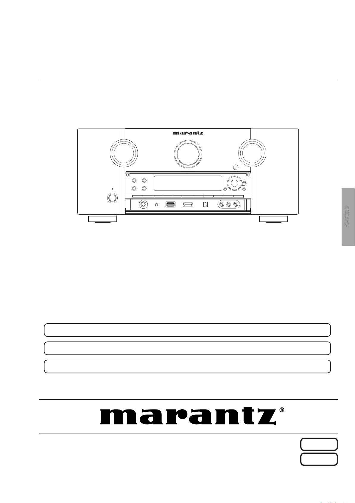
Marantz AV-7005 Service Manual
Service
AV7005 /
N1B/U1B
Manual
AV Pre Tuner
AV7005
For purposes of improvement, specications and design are subject to change without notice.
•
Please use this service manual with referring to the operating instructions without fail.
•
Some illustrations using in this service manual are slightly different from the actual set.
•
AV7005
S0195-1V03DM/DG1011
Copyright 2010 D&M Holdings Inc. All rights reserved.
WARNING: Violators will be prosecuted to the maximum extent possible.
Ver. 3
Please refer to the
MODIFICATION NOTICE.

MARANTZ DESIGN AND SERVICE
Using superior design and selected high grade components,
Only original
MARANTZ
parts can insure that your
MARANTZ
MARANTZ
product will continue to perform to the specifi cations for
company has created the ultimate in stereo sound.
which it is famous.
Parts for your
MARANTZ
ORDERING PARTS :
equipment are generally available to our National Marantz Subsidiary or Agent.
Parts can be ordered either by mail or by Fax.. In both cases, the correct part number has to be specifi ed.
The following information must be supplied to eliminate delays in processing your order :
1. Complete address
2. Complete part numbers and quantities required
3. Description of parts
4. Model number for which part is required
5. Way of shipment
6. Signature : any order form or Fax. must be signed, otherwise such part order will be considered as null and void.
USA
MARANTZ AMERICA, INC
100 CORPORATE DRIVE
MAHWAH, NEW JERSEY 07430
USA
JAPAN
D&M Holdings Inc.
D&M BUILDING, 2-1 NISSHIN-CHO,
KAWASAKI-KU, KAWASAKI-SHI,
KANAGAWA, 210-8569 JAPAN
EUROPE / TRADING
D&M EUROPE B. V.
P. O. BOX 8744, BUILDING SILVERPOINT
BEEMDSTRAAT 11, 5653 MA EINDHOVEN
THE NETHERLANDS
PHONE : +31 - 40 - 2507844
FAX : +31 - 40 - 2507860
CANADA
D&M Canada Inc.
5-505 APPLE CREEK BLVD.
MARKHAM, ONTARIO L3R 5B1
CANADA
PHONE : 905 - 415 - 9292
FAX : 905 - 475 - 4159
KOREA
D&M SALES AND MARKETING KOREA LTD.
2F,YEON BLDG.,
88-5, BANPO-DONG, SEOCHO-GU,
SEOUL KOREA
PHONE : +82 - 2 - 715 - 9041
FAX : +82 - 2 - 715 - 9040
CHINA
D&M SALES AND MARKETING SHANGHAI LTD.
ROOM.808 SHANGHAI AIRPORT CITY TERMINAL
NO.1600 NANJING (WEST) ROAD, SHANGHAI,
CHINA. 200040
TEL : 021 - 6248 - 5151
FAX : 021 - 6248 - 4434
NOTE ON SAFETY :
Symbol z Fire or electrical shock hazard. Only original parts should be used to replaced any part marked with symbol z .
Any other component substitution (other than original type), may increase risk of fi re or electrical shock hazard.
安全上の注意:
zがついている部品は、安全上重要な部品です。必ず指定されている部品番号の部品を使用して下さい。
SHOCK, FIRE HAZARD SERVICE TEST :
CAUTION : After servicing this appliance and prior to returning to customer, measure the resistance between either primary
AC cord connector pins (with unit NOT connected to AC mains and its Power switch ON), and the face or Front Panel of
product and controls and chassis bottom.
Any resistance measurement less than 1 Megohms should cause unit to be repaired or corrected before AC power is applied,
and verifi ed before it is return to the user/customer.
Ref. UL Standard No. 60065.
In case of diffi culties, do not hesitate to contact the Technical
Department at above mentioned address.
2
091105DM/DG

SAFETY PRECAUTIONS
The following check should be performed for the continued protection of the customer and service technician.
LEAKAGE CURRENT CHECK
Before returning the unit to the customer, make sure you make either (1) a leakage current check or (2) a line to chassis
resistance check. if the leakage current exceeds 0.5 milliamps, or if the resistance from chassis to either side of the
power cord is less than 460 kohms, the unit is defective.
Be sure to test for leakage current with the AC plug in both polarities, in addition, in each power ON, OFF and STANDBY
mode, if applicable.
CAUTION
Please heed the points listed below during servicing and inspection.
◎Heed the cautions!
Spots requiring particular attention when servicing, such
as the cabinet, parts, chassis,etc., have cautions indicated
on labels. be sure to heed these causions and the
cautions indicated in the handling instructions.
◎Caution concerning electric shock!
(1) An AC voltage is impressed on this set, so touching
internal metal parts when the set is energized could
cause electric shock. Take care to avoid electric
shock, by for example using an isolating transformer
and gloves when servicing while the set is energized,
unplugging the power cord when replacing parts, etc.
(2) Tere are high voltage parts inside. Handle with extra
care when the set is energized.
◎ Caution concerning disassembly and
assembly!
Through great care is taken when manufacturing parts
from sheet metal, there may in some rare cases be burrs
on the edges of parts which could cause injury if fi ngers
are moved across them. Use gloves to protect your hands.
◎Only use designated parts!
The set's parts have specific safety properties (fire
resistance, voltage resistance, etc.). For replacement
parts, be sure to use parts which have the same
poroperties. In particular, for the important safety parts
that are marked z on wiring diagrams and parts lists, be
sure to use the designated parts.
◎ Be sure to mount parts and arrange the wires
as they were originally!
For safety seasons, some parts use tape, tubes or other
insulating materials, and some parts are mounted away
from the surface of printed circuit boards. Care is also
taken with the positions of the wores omsode amd clamps
are used to keep wires away from heating and high
voltage parts, so be sure to set everything back as it was
originally.
◎Inspect for safety after servicing!
Check that all screws, parts and wires removed or
disconnected for servicing have been put back in their
original positions, inspect that no parts around the area
that has been serviced have been negatively affected,
conduct an inslation check on the external metal
connectors and between the blades of the power plug,
and otherwise check that safety is ensured.
(Insulation check procedure)
Unplug the power cord from the power outlet, disconnect
the antenna, plugs, etc., and turn the power switch on.
Using a 500V insulation resistance tester, check that the
inplug and the externally exposed metal parts (antenna
terminal, headphones terminal, input terminal, etc.) is
1MΩ or greater. If it is less, the set must be inspected and
repaired.
CAUTION
Concerning important safety
parts
Many of the electric and structural parts used in the set
have special safety properties. In most cases these
properties are difficult to distinguish by sight, and using
replacement parts with higher ratings (rated power and
withstand voltage) does not necessarily guarantee that
safety performance will be poreserved. Parts with safety
properties are indicated as shown below on the wiring
diagrams and parts lists is this service manual. Be sure to
replace them with parts with the designated part number.
(1) Schematic diagrams ...... Indicated by the z mark.
(2) Parts lists ...... Indicated by the z mark.
Using parts other than the designated
parts could result in electric shock, fi res
or other dangerous situations.
3
NOTE FOR SCHEMATIC DIAGRAM
WARNING:
Parts marked with this symbol z have critical characteristics. Use ONLY replacement parts recommended by the manufacture
CAUTION:
Before returning the unit to the customer, make sure you make either (1) a leakage current check or (2) a line to chassis resistance check. If the
leakage current exceeds 0.5 milliamps, or if the resistance from chassis to either side of the power cord is less than 460 kohms, the unit is defective.
WARNING:
DO NOT return the unit to the customer until the problem is located and corrected.
NOTICE:
ALL RESISTANCE VALUES IN OHM. k=1,000 OHM / M=1,000,000 OHM
ALL CAPACITANCE VALUES IN MICRO FARAD. P=MICRO-MICRO FARAD EACH VOLTAGE AND CURRENT ARE MEASURED AT NO SIGNAL
INPUT CONDITION. CIRCUIT AND PARTS ARE SUBJECT TO CHANGE WITHOUT PRIOR NOTICE.
r.
NOTE FOR PARTS LIST
Parts for which "nsp" is indicated on this table cannot be supplied.
1.
When ordering of part, clearly indicate "1" and "I" (i) to avoid mis-supplying.
2.
3.
Ordering part without stating its part number can not be supplied.
4.
Part indicated with the mark "★" is not illustrated in the exploded view.
5.
Not including General-purpose Carbon Film Resistor in the P.W.Board parts list. (Refer to the Schematic Diagram for those parts.)
6.
Not including General-purpose Carbon Chip Resistor in the P.W.Board parts list. (Refer to the Schematic Diagram for those parts.)
WARNING:
● Resistors
Ex.: RN
* Resistance
● Capacitors
Ex.: CE
* Capacity (electrolyte only)
* Capacity (except electrolyte)
・ When the dielectric strength is indicated in AC,"AC" is included after the dieelectric strength value.
Parts marked with this symbol z have critical characteristics. Use ONLY replacement parts recommended by the manufacturer.
14K
Type
Shape
and performance
RD : Carbon
RC : Composition
RS : Metal oxide film
RW: winding
RN : Metal film
RK : Metal mixture
2
Indicates number of zeros after effective number.
2-digit effective number.
1-digit effective number.
: Units: ohm
CE : Aluminum foil
electrolytic
CA : Aluminium solid
electrolytic
CS : Tantalum electrolytic
CQ: Film
CK : Ceramic
CC : Ceramic
CP : Oil
CM: Mica
CF : Metallized
CH : Metallized
・ Units:μF.
・ Units:pF
2-digit effective number, decimal point indicated by R.
04W
Type
Shape
and performance
2
Indicates number of zeros after effective number.
2-digit effective number.
2
Indicates number of zeros after efective number. (More than 2)
2-digit effective number.
2E
Power
2B : 1/8 W
2E : 1/4 W
2H : 1/2 W
3A : 1 W
3D : 2 W
3F : 3 W
3H : 5 W
1800ohm=1.8kohm1 8
1.2ohm1 R 2
1H
Dielectric
strength
0J : 6.3 V
1A : 10 V
1C : 16 V
1E : 25 V
1V : 35 V
1H : 50 V
2A : 100 V
2B : 125 V
2C : 160 V
2D : 200 V
2E : 250 V
2H : 500 V
2J : 630 V
2200μF2 2
2200pF=0.0022μF2 2
182
Resistance
F:±1%
G:±2%
J:±5%
K:±10%
M:±20%
3R2
CapacityMAllowable
G
Allowable
error
P : Pulse-resistant type
NL : Low noise type
NB : Non-burning type
FR : Fuse-resistor
F : Lead wire forming
error
F:±1%
G:±2%
J:±5%
K:±10%
M:±20%
Z:±80%
:- 20%
P : +100%
C:±0.25pF
D:±0.5pF
= : Others
FR
Others
BP
Others
HS : High stability type
BP : Non-polar type
HR : Ripple-resistant type
DL : For change and discharge
HF : For assuring high requency
U : UL part
C : CSA part
W : UL-CSA part
F : Lead wire forming
2
・ Units:μF.
1
・ Units:pF
2.2μF2 R
1-digit effective number.
2-digit effective number, decimal point indicated by R
220pF2 2
Indicates number of zeros after effective numver. (0 or 1)
2-digit effective number.
4
TECHNICAL SPECIFICATIONS
n Audio Section
• Analog
Input sensitivity/Input impedance : 200 mV/47 kΩ
Frequency response : 10 Hz – 100 kHz — +1, –3 dB (DIRECT mode)
S/N : 105 dB (IHF–A weighted, DIRECT mode)
Distortion : 0.005 % (20 Hz ~ 20 kHz) (DIRECT mode)
Rated output : Unbalanced pre-output: 1.2 V
• Digital
D/A output : Rated output — 2 V (at 0 dB playback)
Total harmonic distortion — 0.008 % (1 kHz, at 0 dB)
S/N ratio — 102 dB
Dynamic range — 100 dB
Digital input : Format — Digital audio interface
• Phono equalizer (PHONO input — REC OUT)
Input sensitivity : 2.5 mV
RIAA deviation : ±1 dB (20 Hz to 20 kHz)
S/N : 74 dB (A weighting, with 5 mV input)
Rated output : 150 mV
Distortion factor : 0.03 % (1 kHz, 3 V)
n Video Section
• Standard video connectors
Input/output level and impedance : 1 Vp-p, 75 Ω
Frequency response : 5 Hz – 10 MHz — +1, –3 dB
• Color component video connector
Input/output level and impedance:
Y (brightness) signal — 1 Vp-p, 75 Ω
B / CB signal — 0.7 Vp-p, 75 Ω
P
R / CR signal — 0.7 Vp-p, 75 Ω
P
Frequency response :
5 Hz – 60 MHz — +0, –3 dB (when “Video Convert” set to “OFF”)
Balanced pre-output: 2.4 V
n Tuner section (for U)
[FM](Note: μV at 75 Ω, 0 dBf = 1 x 10
Receiving Range :
[FM] 87.5 MHz – 107.9 MHz
Usable Sensitivity :
[FM]1.5 μV (14.8 dBf)
S/N (IHF-A) :
[FM]MONO 78 dB
STEREO 68 dB
HD 85 dB
Total harmonic Distortion (at 1 kHz) :
[FM]MONO 0.1 %
STEREO 0.2 %
HD 0.02 %
[AM]18 μV
[AM]
85 dB
[AM]
0.02 %
n Tuner section (for N)
[FM](Note: μV at 75 Ω, 0 dBf = 1 x 10
Receiving Range :
[FM] 87.5 MHz – 108.0 MHz [AM]522 kHz – 1611 kHz
Usable Sensitivity :
[FM]1.2 μV (12.8 dBf) [AM]18 μV
S/N (IHF-A) :
[FM]MONO 72 dB
STEREO 67 dB
Total harmonic Distortion (at 1 kHz) :
[FM]MONO 0.3 %
STEREO 0.7 %
–15
W)
[AM]530 kHz – 1710 kHz
–15
W)
n General
Power supply (for U) : AC 120 V, 60 Hz
Power supply (for N) : AC 230 V, 50 Hz
Power consumption :
60 W
0.2 W (Standby)
4.0 W (CEC standby)
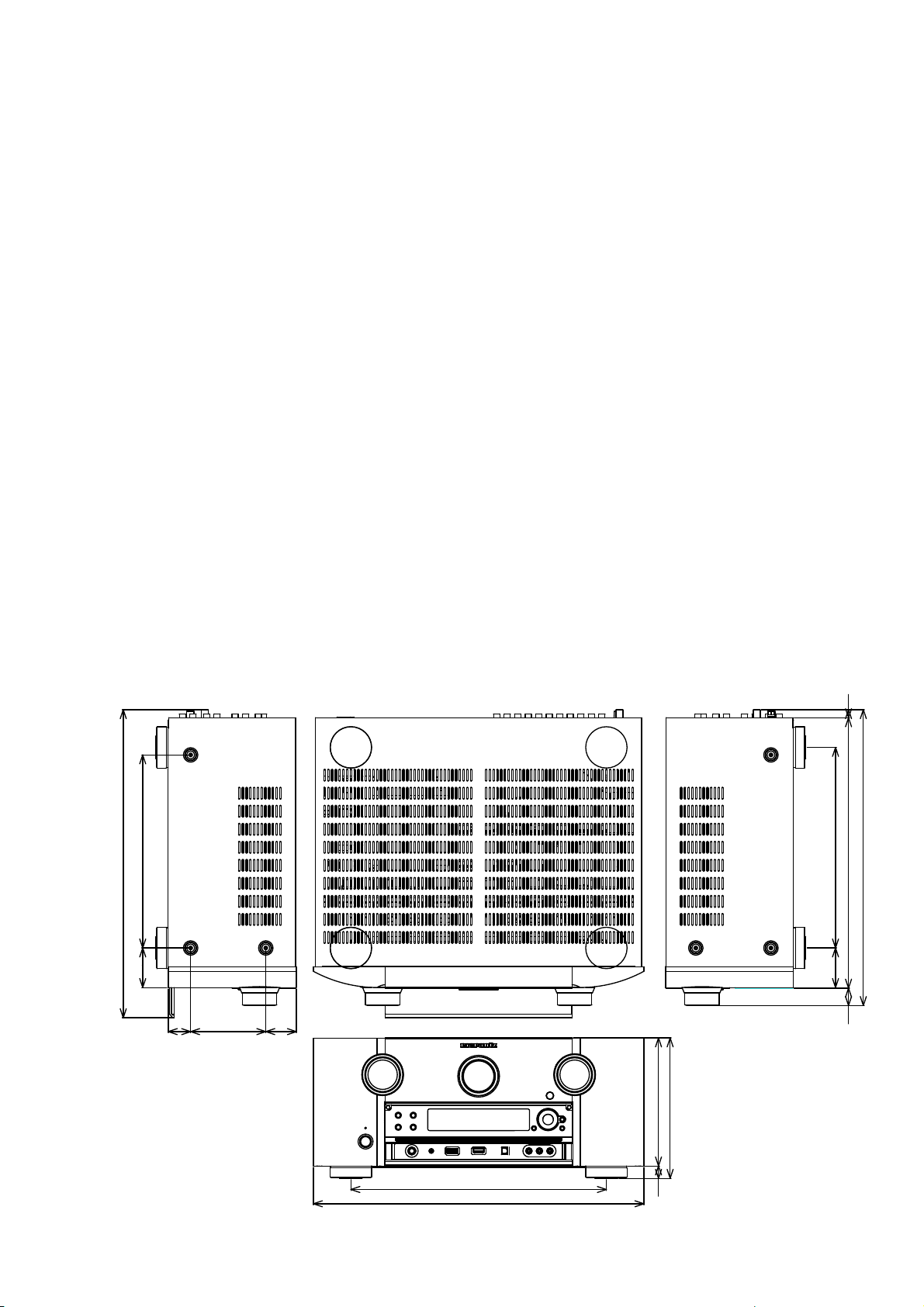
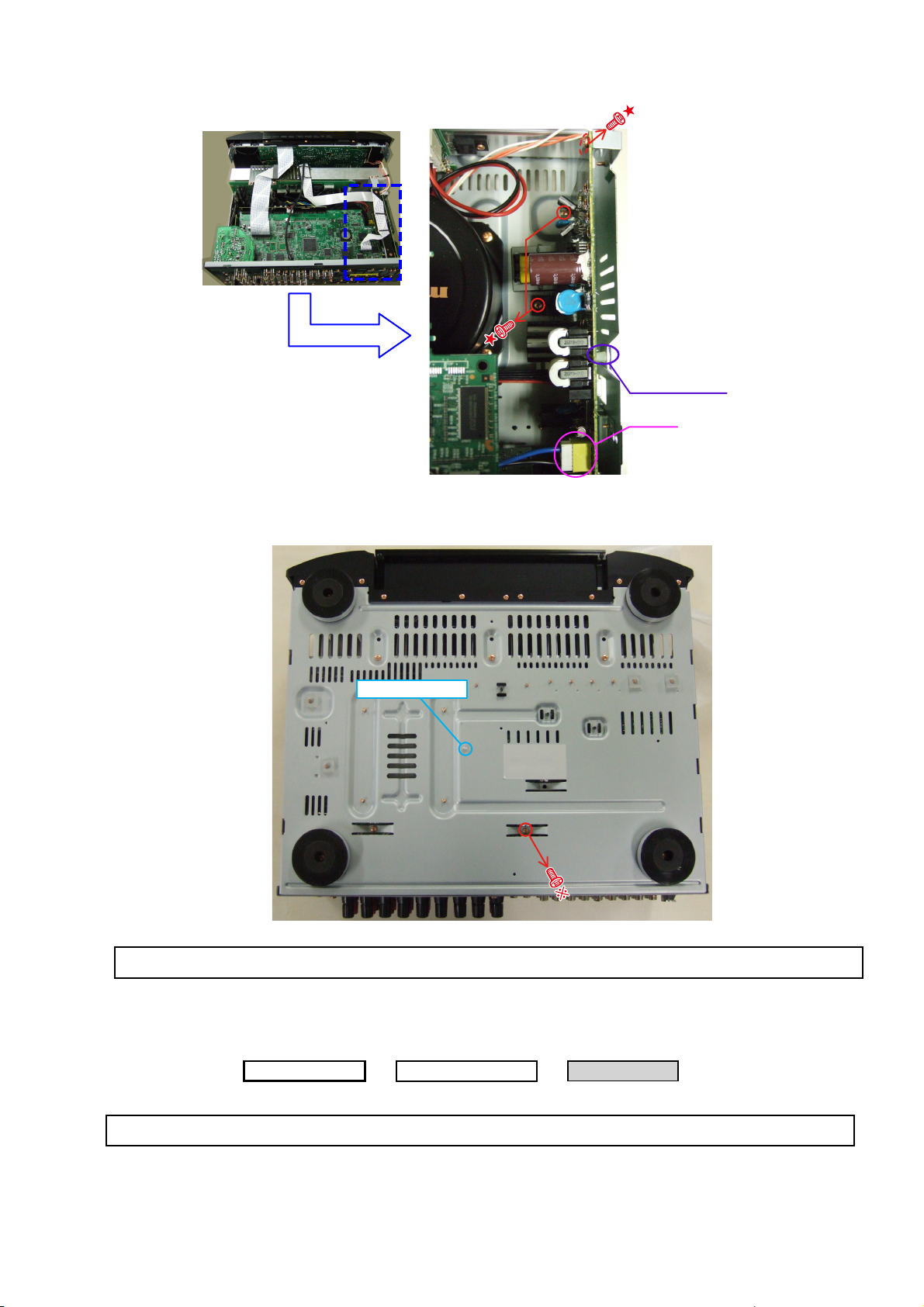
Maximum external dimensions : 440 (W) x 187 (H) x 395 (D) mm
Weight : 10.1 kg
n Remote Control Unit (RC011SR)
Batteries : R03/AAA Type (two batteries)
DIMENSION
257
412
52.7
29.8
100
40.7
11. 5
395
360
267
52.7
23.5
170.5
340
440
187
16.5
5
CAUTION IN SERVICING
Firmware update
• When you replace the DIGITAL UNIT ASSY (8U-310051E), you need software updates.
Refer to "VERSION UPGRADE PROCEDURE OF FIRMWARE (26 - 36 page) .
Please update the following procedure.
1. First, Please update by DFW (33 - 36 page).
2. Next, Please update the latest fi rmware by DPMS (26 - 32 page).
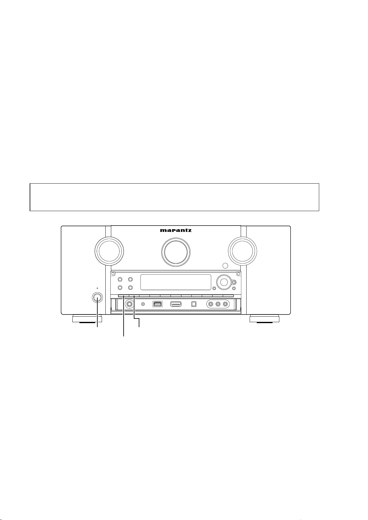
Initializing AV Pre Tuner
AV Pre Tuner initialization should be performed when the μcom, peripheral parts of μcom, and Digital P.W.B. are
replaced.
1. Turn off the power using ON/STANDBY button.
2. Press ON/STANDBY button while simultaneously pressing SURROUND MODE and AUTO buttons.
3. Check that the entire display is fl ashing with an interval of about 1 second, and release your fi ngers from the 2
buttons and the microprocessor will be initialized.
Note: •If step 3 does not work, start over from step 1.
All user settings will be lost and this factory setting will be recovered when this initialization mode.
•
So make sure to memorize your setting for restoring after the initialization.
ON/STANDBY
AUTO
SURROUND MODE
Service Jigs
When you repair the printing board, you can use the following JIG (Extension cable kit).
Please order to marantz Offi cial Service Distributor in your region if necessary.
8U-110084S : EXTENSION UNIT KIT : 1 Set
(Refer to "JIG FOR SER
VICING".)
6
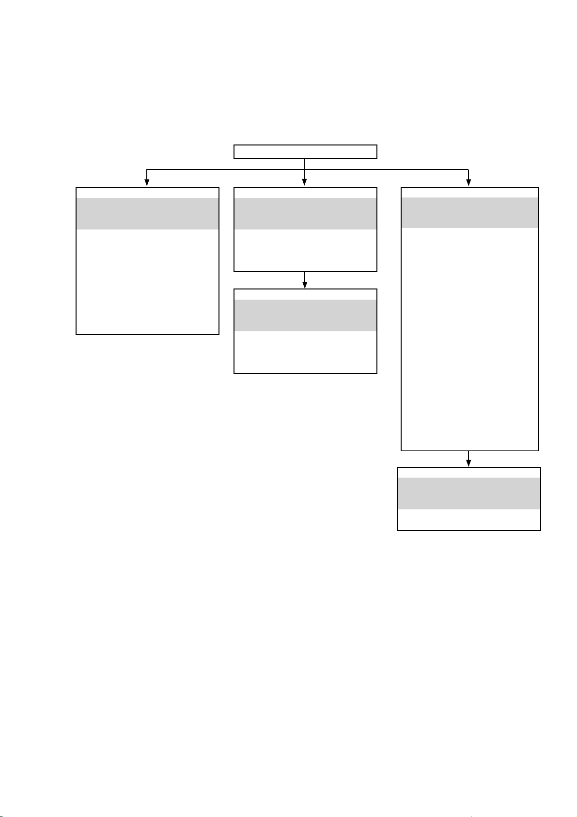
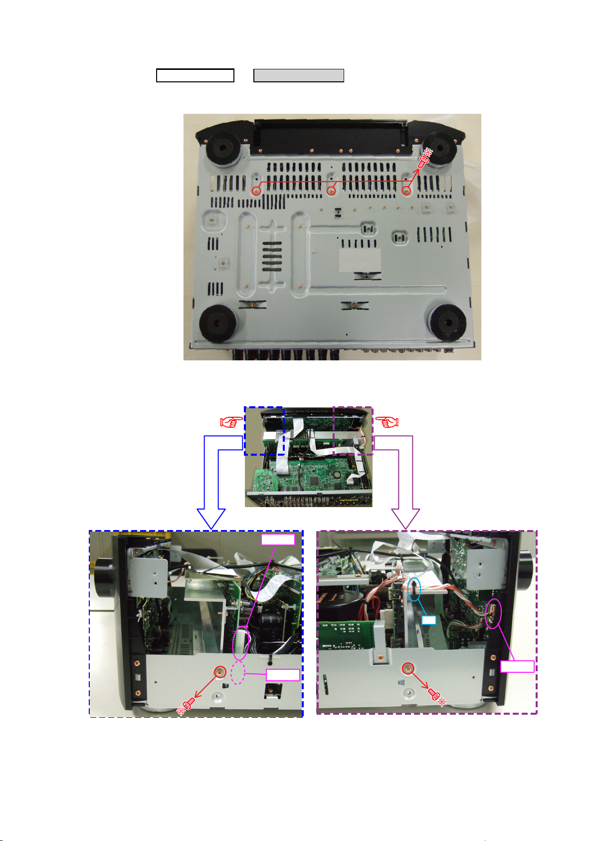
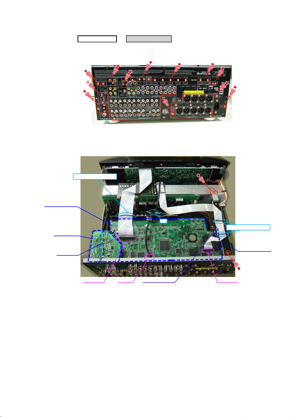
DISASSEMBLY
• Disassemble in order of the arrow of the fi gure of following fl ow.
• In the case of the re-assembling, assemble it in order of the reverse of the following fl ow.
• In the case of the re-assembling, observe "attention of assembling" it.
• If wire bundles are untied or moved to perform adjustment or parts replacement etc., be sure to rearrange them neatly
as they were originally bundled or placed afterward.
Otherwise, incorrect arrangement can be a cause of noise generation.
CABINET TOP
FRONT PANEL ASSY
Refer to "DISASSEMBLY
1. FRONT PANEL ASSY"
and "EXPLODED VIEW"
FRONT UNIT ASSY
(Ref. No. of EXPLODED VIEW : P1)
OPT UNIT
(Ref. No. of EXPLODED VIEW : P2)
H/P UNIT
(Ref. No. of EXPLODED VIEW : P3)
FRONT HDMI UNIT
(Ref. No. of EXPLODED VIEW : P4)
DOORDET UNIT
(Ref. No. of EXPLODED VIEW : P5)
HEAT SINK ASSY
Refer to "DISASSEMBLY
2. HEAT SINK ASSY"
and "EXPLODED VIEW"
GUIDE TOP UNIT
(Ref. No. of EXPLODED VIEW : P21)
HDAM AMP UNIT
(Ref. No. of EXPLODED VIEW : P23)
PCB REG CNT/PCB REG
Refer to "DISASSEMBLY
3. PCB REG CNT/PCB REG"
and "EXPLODED VIEW"
REG UNIT
(Ref. No. of EXPLODED VIEW : P8)
REG-CNT UNIT
(Ref. No. of EXPLODED VIEW : P9)
HDMI UNIT ASSY
Refer to "DISASSEMBLY
4. HDMI UNIT ASSY"
and "EXPLODED VIEW"
FRONT CNT UNIT
(Ref. No. of EXPLODED VIEW : P10)
INPUT UNIT
(Ref. No. of EXPLODED VIEW : P11)
A.AUDIO UNIT
(Ref. No. of EXPLODED VIEW : P13)
VIDEO UNIT ASSY
(Ref. No. of EXPLODED VIEW : P14)
DIGITAL UNIT
(Ref. No. of EXPLODED VIEW : P15)
SIDE-CNT UNIT
(Ref. No. of EXPLODED VIEW : P17)
RS232C UNIT
(Ref. No. of EXPLODED VIEW : P18)
SIRIUS UNIT
(Ref. No. of EXPLODED VIEW : P19)
XLR CONNECT UNIT
(Ref. No. of EXPLODED VIEW : P24)
BALANCE OUT UNIT
(Ref. No. of EXPLODED VIEW : P25)
TRANS MAIN
Refer to "DISASSEMBLY
5. TRANS MAIN"
and "EXPLODED VIEW"
TRANS MAIN
(Ref. No. of EXPLODED VIEW : P22)
7
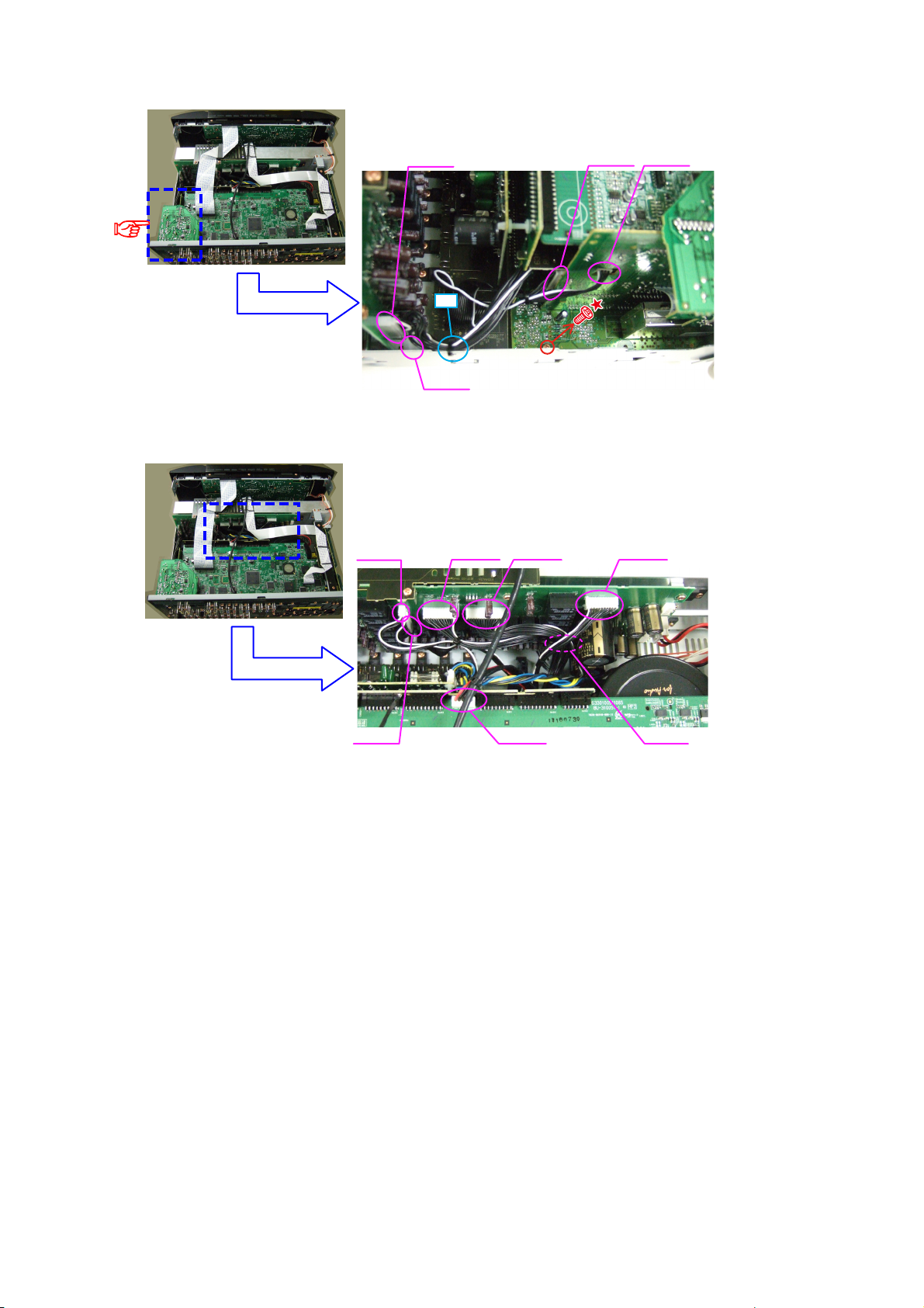
About the photos used for descriptions in the DISASSEMBLY" section.
• The direction from which the photographs used herein were photographed is indicated at "Direction of photograph: ***"
at the left of the respective photographs.
• Refer to the table below for a description of the direction in which the photos were taken.
• Photographs for which no direction is indicated were taken from above the product.
The viewpoint of each photograph
(Photografy direction)
[View from above]
Direction of photograph: C
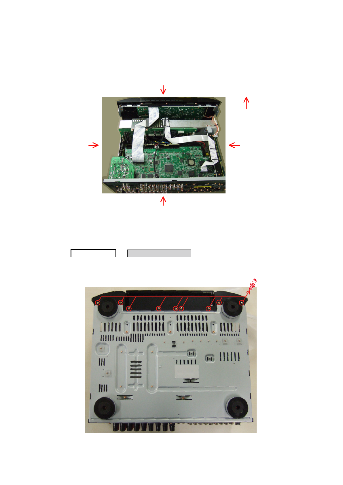
1. FRONT PANEL ASSY
Direction of photograph: B
Front side
Direction of photograph: D
Direction of photograph: A
Proceeding :
(1) Remove the screws.
View from bottom
CABINET TOP
FRONT PANEL ASSY
→
8
(2) Cut the wire clamp band, then disconnect the connector wires and FFC cable.
STYLEPIN : Loose
FFC cable
N4201
N1001
STYLEPIN : Loose
cut
FFC cable
Do not remove the FERRITE CORE when you disconnect the FFC cable.
b
FERRITE CORE
9
(3) Remove the screws.
Direction of
photograph: C
Please refer to "EXPLODED VIEW" for the disassembly method of each P.W.B included in FRONT PANEL ASSY.
Direction of
photograph: D
10
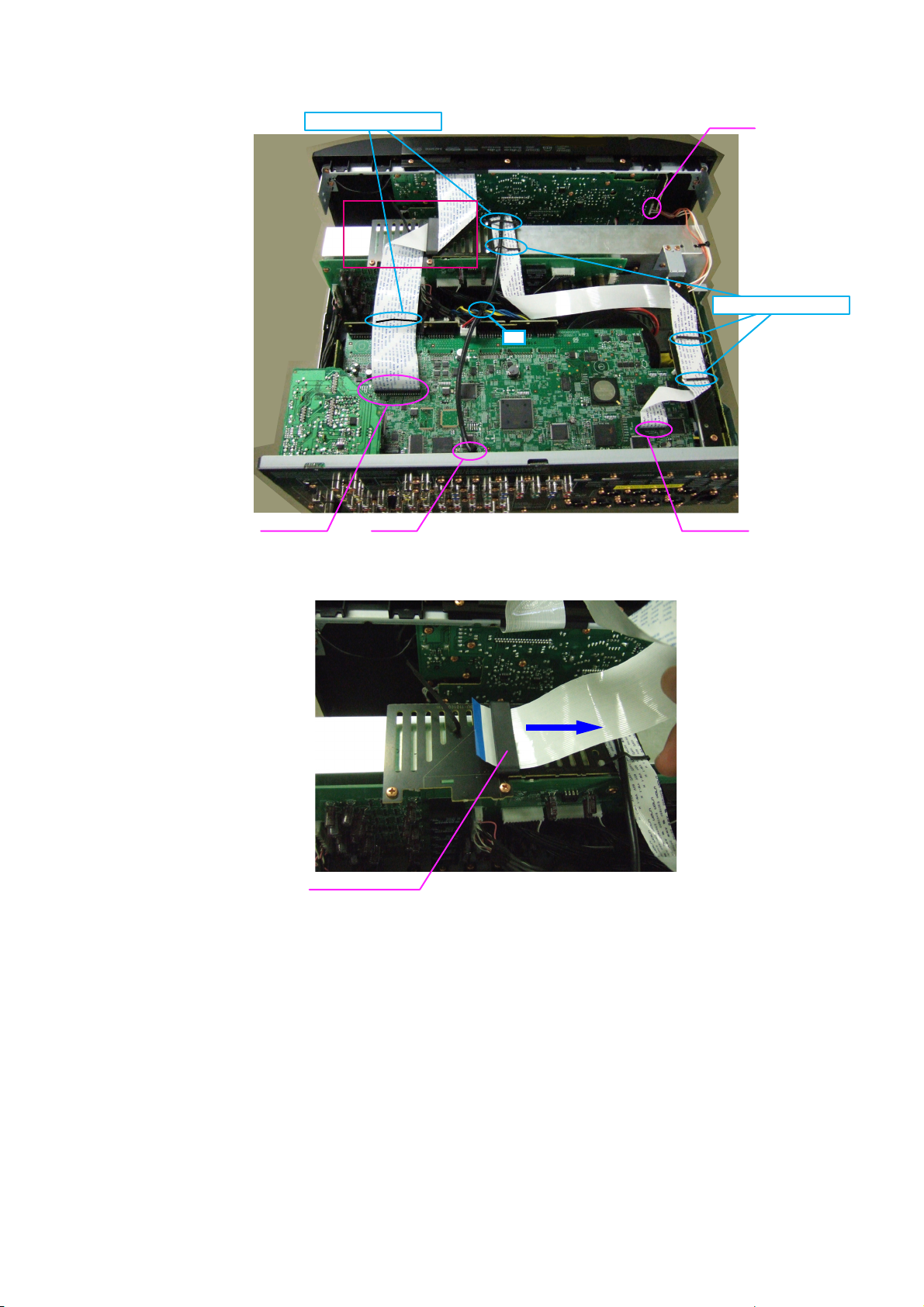
2. HEAT SINK ASSY
Proceeding :
(1) Remove the screws.
View from bottom
CABINET TOP
HEAT SINK ASSY
→
(2) Cut wire clamp band, then remove the screws. Disconnect the connector wires.
Direction of
photograph: C
N4001
N4002
Direction of
photograph: D
cut
N1001
11
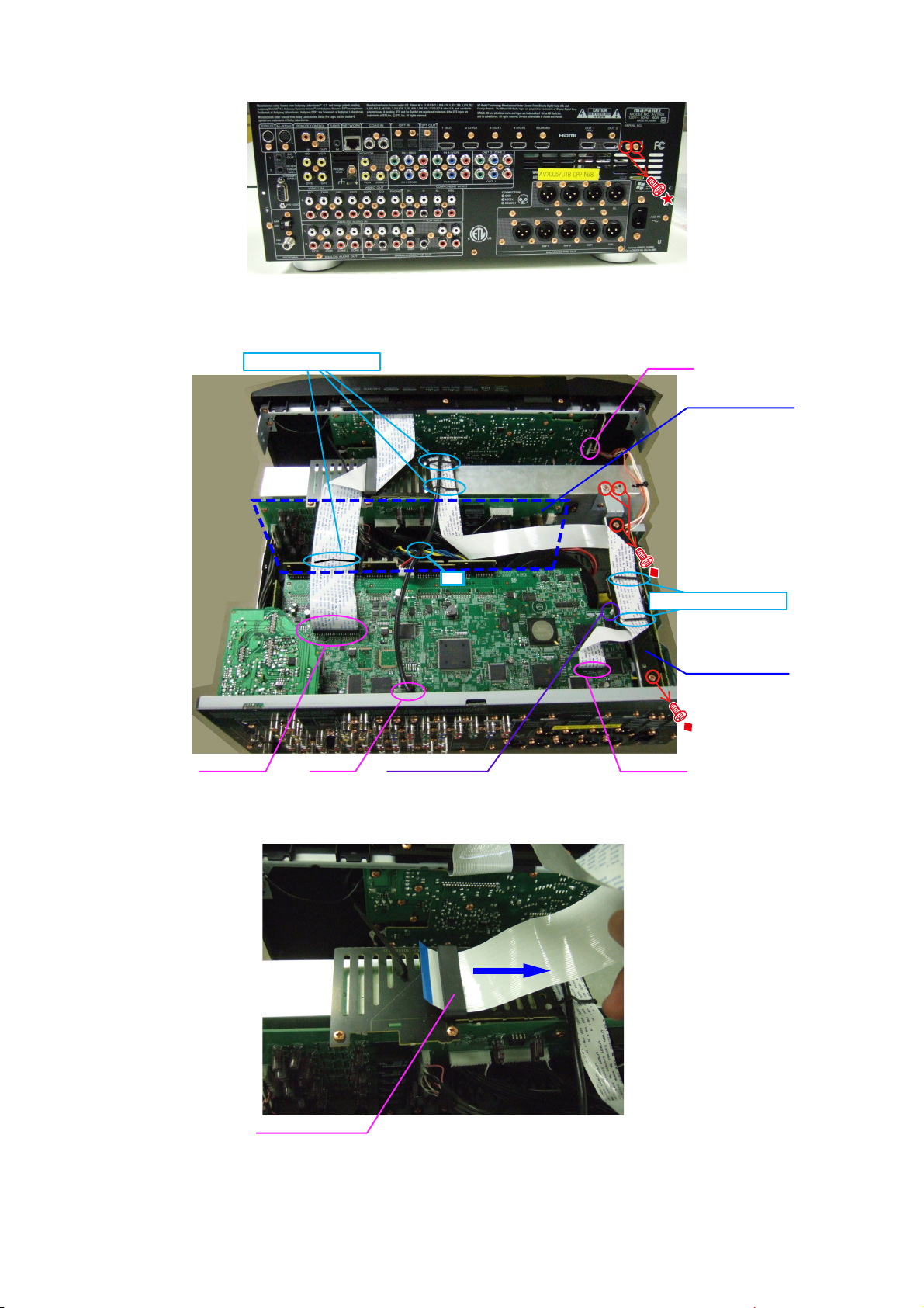
(3) Remove the screws.
Direction of photograph: A
(4) Cut the wire clamp bands, then disconnect the connector wires and FFC cable. Remove the screws, SUPPORT
PWB. and the HDMI BRACKET.
STYLEPIN : Loose
FFC cable
N4201
cut
SUPPORT P.W.B.
N1001
HEATSINK ASSY
STYLEPIN : Loose
HDMI BRACKET
FFC cable
Do not remove the FERRITE CORE when you disconnect the FFC cable.
b
FERRITE CORE
12
(5) Disconnect the connector wires.
N4006
Please refer to "EXPLODED VIEW" for the disassembly method of each P.W.B included in HEAT SINK ASSY.
N4008N4004N4003
N8003N4009N4005
13
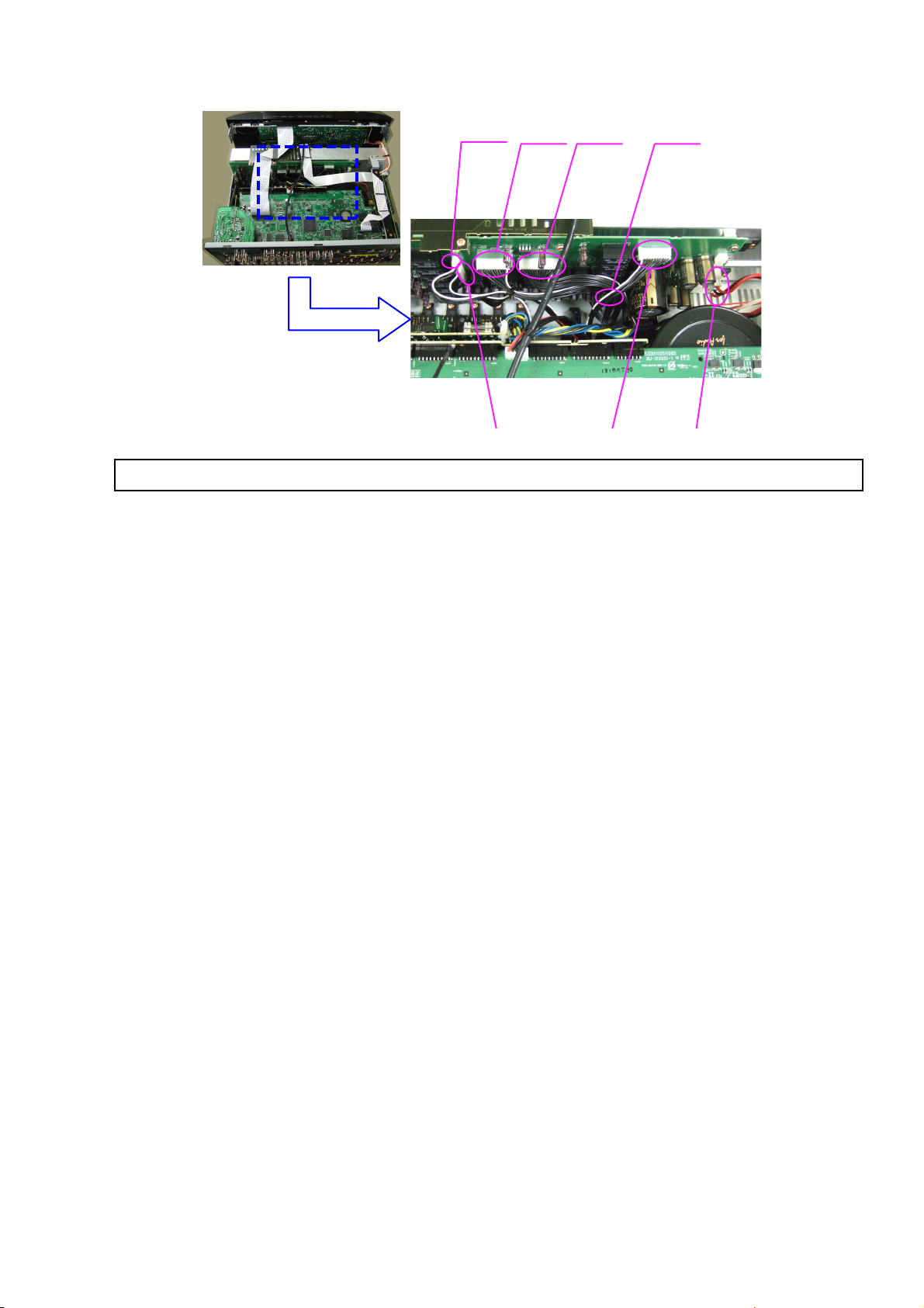
3. PCB REG CNT/PCB REG
Proceeding :
(1) Remove the screws.
CABINET TOP
PCB REG
HEAT SINK ASSY
→
N model
PCB REG CNT/PCB REG
→
(2) Disconnect the connector wires and connector board.
CP102
Direction of photograph: C
CP104
Board to board
REG CNT UNIT
N2004
CP13A
14
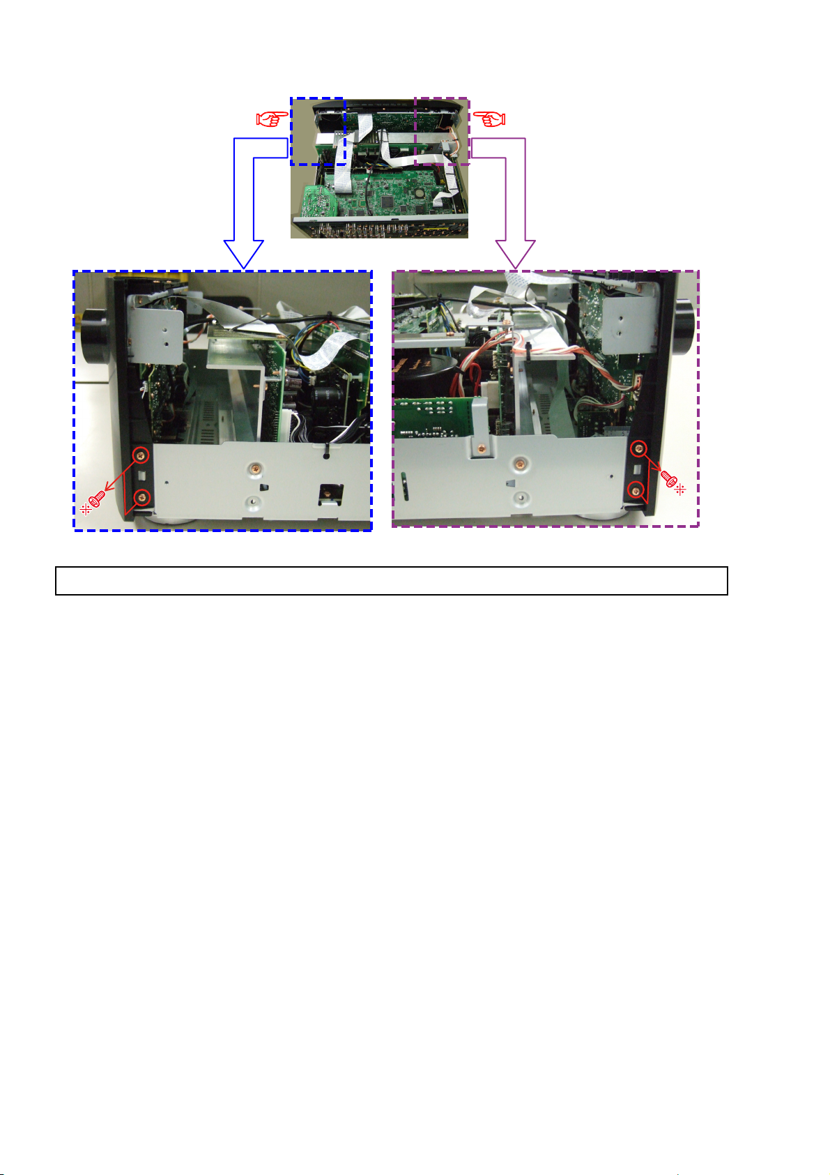
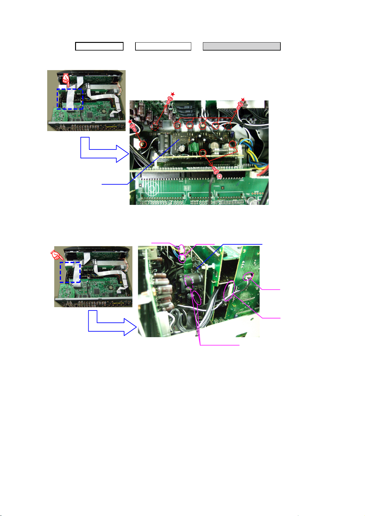
4. HDMI UNIT ASSY
Proceeding :
(1) Remove the screws, then remove the BACK PANEL and the HDMI BRACKET.
Direction of photograph: A
(2) Cut wire clamp band, then disconnect the connector wires and the FFC cables. Remove the screws and the
SUPPORT PWB.
Remove the PCB SIRIUS and the PCB RS232 from the PCB SIDE CNT(Board to board).
CABINET TOP
U model
STYLEPIN : Loose
HDMI UNIT ASSY
→
HDMI UNIT ASSY
SIRIUS UNIT
232C UNIT
FFC cable
N4201
cut
SUPPORT P.W.B.
STYLEPIN : Loose
HDMI BRACKET
FFC cable
15
(3) Cut the wire clamp band, then disconnect the connector wires. Remove the screw.
Direction of photograph: C
(4) Disconnect the connector.
N4006
N4001
cut
N4002
N4003 N4004
N2004CP13A
N4009
Direction of photograph: D
N4005
N4008N4610
16
(5) Disconnect the connector wire, then remove the screws and the P.W.B HOLDER..
Direction of photograph: D
P.W.B. HOLDER
CX102
(6) Remove the screws and P.W.B HOLDER. Remove the HDMI UNIT ASSY from the main unit.
P.W.B HOLDER
View from bottom
Please refer to "EXPLODED VIEW" for the disassembly method of each P.W.B included in HDMI UNIT ASSY.
5. TRANS MAIN
Proceeding :
Please refer to "EXPLODED VIEW" for the disassembly method of each P.W.B included in TRANS MAIN.
CABINET TOP
HDMI UNIT ASSY
→
TRANS MAIN
→
17
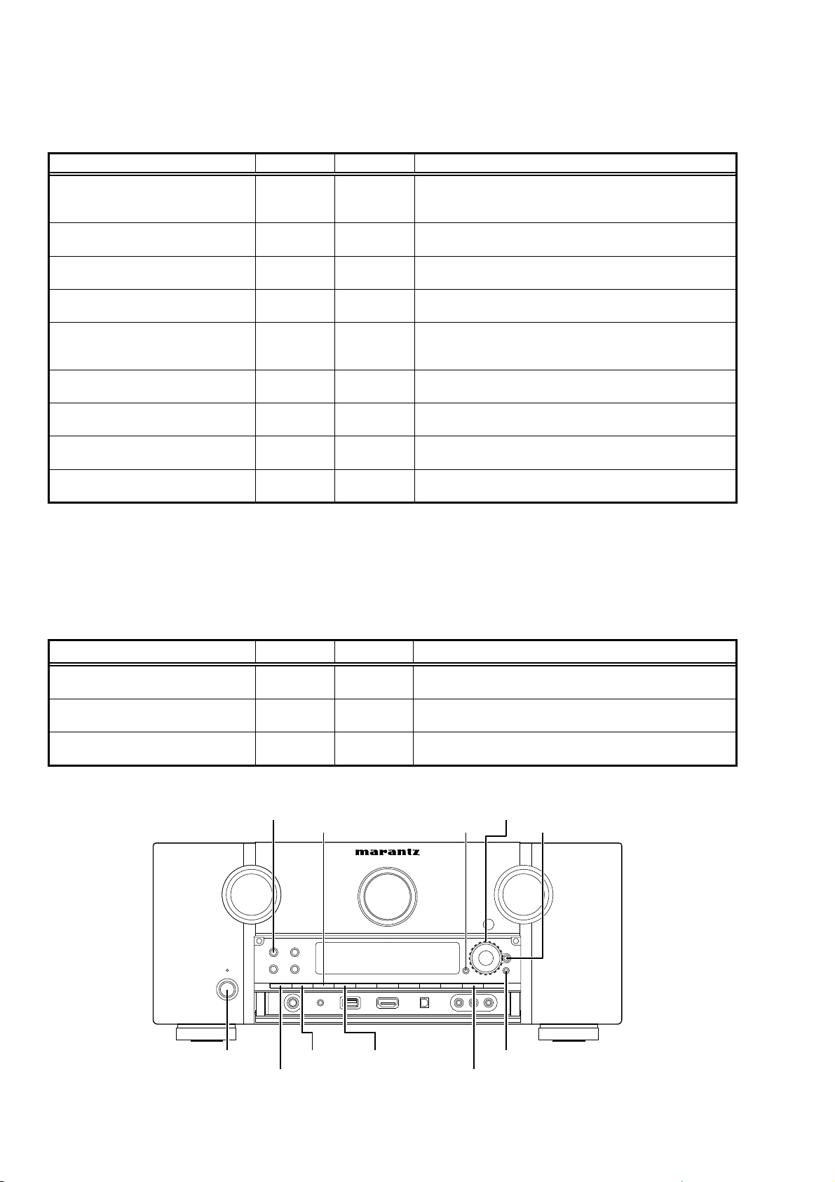
SPECIAL MODE
Special mode setting button
Press the ON/STANDBY button to turn on while pressing both buttons A and B at the same time.
b
Mode Button A Button B Contents
Firmware versions such as Main, Sub, DSP are displayed in
com/DSP Version display mode STATUS RETURN
IInitialization mode
(Remove settings for Installer Setup.)
Initialization mode
(Includes settings for Installer Setup)
Mode for switching tuner frequency step
Mode for preventing remote control
acceptance
Panel lock mode AUTO DISPLAY
Panel lock mode
(Remove Master volume)
Cancellation of panel lock mode
Installer Setup mode MENU
SURROUND
MODE
CURSOR UP
SURROUND
MODE
STATUS ENTER
DISPLAY
CURSOR
DOWN
DIRECT
DIRECT
DIRECT
DISPLAY Panel lock mode is cancelled.
CURSOR
AUTO
PURE
PURE
PURE
LEFT
the FL manager. Errors are displayed when they occur.
(Refer to 17 page.)
Backup data initialization is carried out.
(Remove settings for Installer Setup)
Backup data initialization is carried out.
(Includes settings for Installer Setup)
---N model only--Change tuner frequency step to FM:200kHz/AM:10kHzSTEP
Operations using remote control are rejected.
(Mode cancellation: Turn off power and execute the same
button operations as when performing setup.)
Operations using main unit panel buttons or master volume are
rejected.
Operations using main unit panel buttons are rejected.
Access Remote Maintenance mode via the internet.
InstallerSetup is displayed on GUI/Option Menu.
NOTE:
If " S " is displayed on the fl uorescent display, the unit is set to the special developer's mode and RS-232C
communications are not possible.
Press and hold in the "STATUS" and " i " buttons for over 3 seconds with the power turned on to turn the " S "
display off. RS-232C communications are now enabled.
When power is turned on, pressing both buttons A and B at the same time for 3 seconds or more.
b
Mode Button A Button B Contents
DUAL BACKUP MEMORY (Backup) SLEEP ENTER
DUAL BACKUP MEMORY (Recovery) SLEEP MENU
DUAL BACKUP MEMORY
(Backup Clear)
SLEEP AUTO
Backup of DUAL BACKUP MEMORY is performed.
(Refer to 20 page.)
Recovery of DUAL BACKUP MEMORY is performed.
(Refer to 20 page.)
Backup of DUAL BACKUP MEMORY is cleared.
(Refer to 20 page.)
PURE DIRECT
CURSOR
DISPLAY MENU ENTER
ON/STANDBY
SURROUND MODE SLEEP
18
RETURNAUTO STATUS
1. μcom/DSP Version display mode
1.1. Operation specifi cations
μcom/DSP version display mode:
When started up, the version information is displayed.
Starting up:
With the "RETURN" and "STATUS" buttons pressed, press the "ON/STANDBY" button to turn the power on.
Now, press the "STATUS" button to the display the 2nd item information on the FL Display.
1.2. Display Order
Error information(Refer to 1.3. Error display) qModel destination information wFirmware Package Version
Main -com/ROM version rMain 1st Boot Loader tSub -com/Sub FBL yDSP version uAudio PLD
e
iOSD FPGA Confi g oOSD Program Q0OSD font data Q1Ethernet(DM860) 1st Boot Loader, Hardware ID
Q2Ethernet(DM860) 2nd Boot Loader, Rhapsody Flag Q3Ethernet(DM860) IMAGE Q4Ethernet(DM860)MAC
ADDRESS information Q5HD RADIO SDK/HD RADIO BBP(U model only) Q6MultEQ Pro APP(Displayed when
Audyssey Pro is complete) Q7MultEQ Pro ICL(Displayed when Audyssey Pro is complete
Model destination information :
q
Upper
Lower
AV7005 *
S/N. **********
Firmware Package Version :
w
Upper
Lower
Main -com & ROM version :
e
Upper
Lower
Main 1st Boot Loader :
r
Upper
Lower
Sub -com & Sub FBL :
t
Upper
Lower
DSP ROM :
y
Upper
Lower
Firm. Package
Main :**.**
Main ROM :**.**
Main FBL :**.**
Sub :**.**
Sub FBL :**.**
DSP :**.**
Ver.:****
Audio PLD :
u
Upper
Lower
OSD FPGA Confi g :
i
Upper
Lower
Audio PLD :**.**
OSD Config:
************
19
OSD Program :
o
Upper
Lower
OSD font data :
Q0
Upper
Lower
Ethernet(DM860) 1st Boot Loader, Hardware ID :
Q1
Upper
Lower
Ethernet(DM860) 2nd Boot Loader, Rhapsody Flag :
Q2
Upper
Lower
Ethernet(DM860) IMAGE :
Q3
Upper
Lower
OSD PRG:
************
OSD DAT:
************
*Ethernet FBL
********-AA
*Ethernet SBL
*************-BB
*Ethernet IMG
*************
Ethernet(DM860) MAC ADDRESS information :
Q4
Upper
Lower
HD RADIO SDK/HD RADIO BBP (U model only) :
Q5
Upper
Lower
MultEQ Pro APP(Displayed when Audyssey Pro is complete) :
Q6
Upper
Lower
MultEQ Pro ICL(Displayed when Audyssey Pro is complete) :
Q7
Upper
Lower
*Ethernet MAC
******-******
*HDSDK: **.**
*HDBBP:C0002.000
*MultEQ Pro APP
**.**.**.****
*MultEQ Pro ICL
**.**.**.****
20
1.3. Error display
See the following table for each "Error information" display and its contents (status).
Display order is q,w,e,r,t.
Condition State State
Sub-com NG No response from Sub-com
q
DIR NG No response from DIR
w
When DSP boot, executing DSP reset makes no change to DSP1 FLAG0
port "H".
No change to DSP FLAG0 port "H" before issuing DSP command.
When DSP data read, executing WRITE="L" makes no change to ACK="H".
When DSP data read, executing REQ="L" makes no change to ACK="L".
DSP NG
e
EEPROM NG Error appeared in EEPROM checksum.(*** is a block address number.)
r
Both SUB/DSP
t
/EEPROM OK
When DSP data write, executing WRITE="H" makes no change to ACK="H".
When DSP data write, executing REQ="L" makes no change to ACK="L".
When DSP special code boot, executing DSP reset makes no change to
DSP FLAG0 port "H".
No change to DSP FLAG0 port "H" before issuing DSP special read
command.
No change to DSP FLAG0 port "H" before DSP version read.
SUB ERROR 01
DIR ERROR 01
DSP ERROR 01
DSP ERROR 02
DSP ERROR 03
DSP ERROR 04
DSP ERROR 05
DSP ERROR 06
DSP ERROR 11
DSP ERROR 12
DSP ERROR 13
E2PROM ERR***
(No error display, version display only)
21
2. DUAL BACKUP MEMORY
This product has a Dual Backup Memory function. The conventional Backup functions to memorize, in the EEPROM
(U5302) in the circuit, a current setting of the moment the main power is turned off so that it can be restored when it
is turned ON again. Meanwhile, the DUAL BACKUP MEMORY is capable of memorizing any arbitrary setting that is
confi gured while the product is in operation so as to restore it at any time. When servicing units returned from end-users
for repairs, use this function to back up the current setting (e.g. Tuner Preset). This will enable the units to be returned to
the users after repairs, with the setting unchanged.
NOTE : If end-users use this function, the data will be overwritten.
The contents of the memory do not disappear even if you initialize this unit.
If you want to erase, please refer to 2.2. SERVICE PRECAUTIONS.
2.1. HOW TO OPERATE
-Backup-
(1) Confi gure a setting you would like to save in the MEMORY and hold down the "SLEEP" and "ENTER" buttons on the
Front Panel at the same time for 3 seconds or more.
(2) The FL Display indicates "MEMORY SAVING" while the Backup is being performed.
FLD
(3) The FL Display indicates "COMPLETE" when the Backup is completed.
FLD
-Recovery-
(1) Hold down the "SLEEP" and "MENU" buttons at the same time for 3 seconds or more.
(2) The FL Display indicates "MEMORY LOAD" while the Recovery is being performed.
FLD
(3) After the FL Display indicates "COMPLETE", the product goes into Standby mode. When the power is restored, the
Recovery is completed.
FLD
The FL Display indicates "NO BACKUP" if the DUAL BACKUP MEMORY has not been activated with no data to be
recovered saved in the Memory.
FLD
MEMORY SAVING
COMPLETE
MEMORY LOAD
COMPLETE
NO BACKUP
2.2. SERVICE PRECAUTIONS
When the Flash Rom (U5302) on the HDMI PWB is replaced make sure, in order to maintain consistency with the
Backup Memory, to clear the DUAL BACKUP MEMORY in thefollowing way :
-How to clear the Backup Memory-
(1) Hold down the "SLEEP" and "AUTO" buttons at the same time for 3 seconds or more.
(2) The FL Display indicates "BACKUP CLEAR" while the memory is being cleared.
FLD
(3) After the FL Display indicates "COMPLETE", the operation is completed.
FLD
BACKUP CLEAR
COMPLETE
22
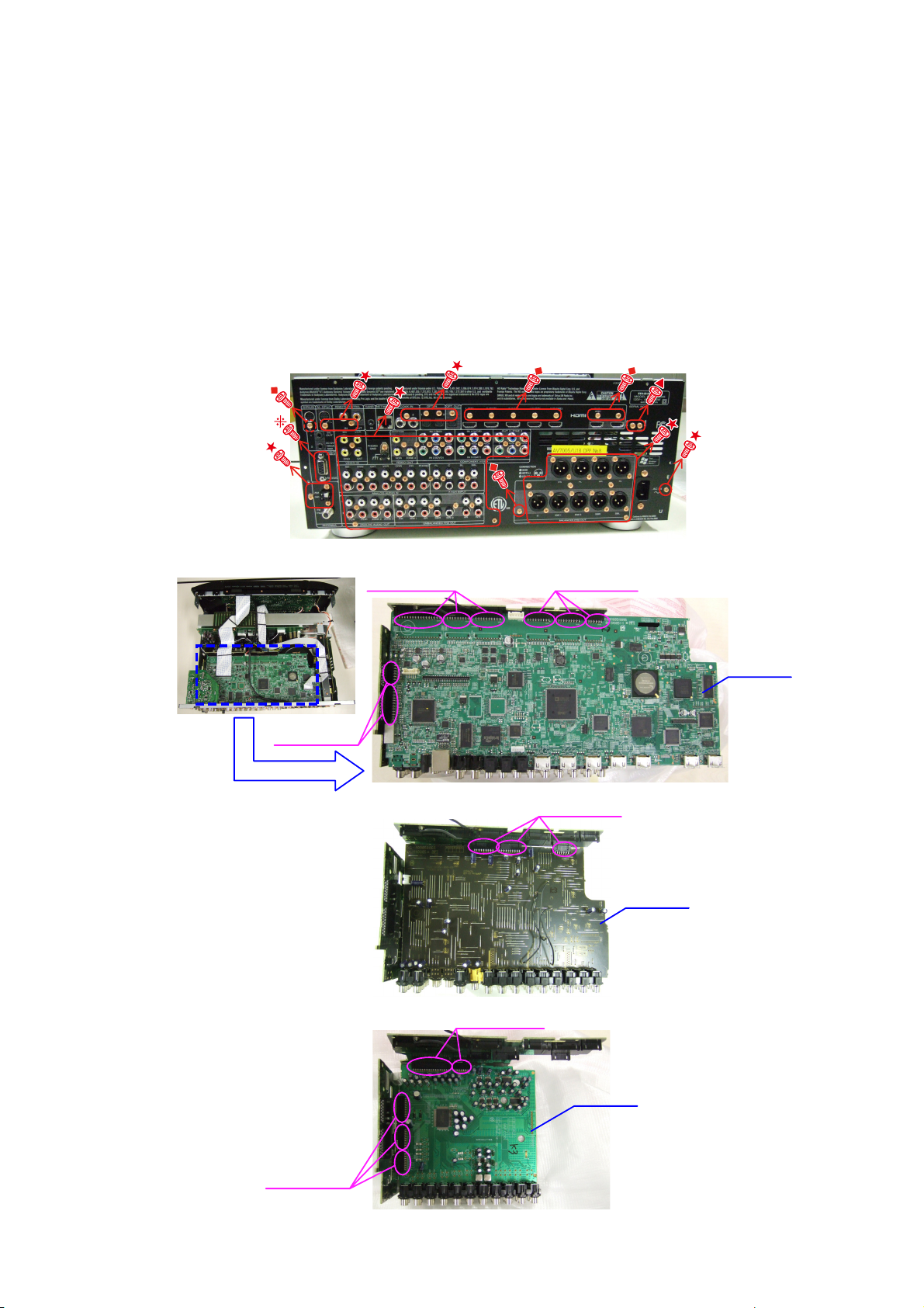
JIG FOR SERVICING
When you repair the printing board, you can use the following JIG (Extension cable kit).
Please order to marantz Offi cial Service. Distributor in your region if necessary.
Note: When the connection which is wrong in the JIG (EXTENSION UNIT KIT) is done it becomes cause of damage.
8U-110084S :
EXTENSION UNIT KIT
• Connection of PCB HDMI JIG
-Preparation-
8U-110084S : EXTENSION UNIT KIT : 1 Set
Insulation sheet (Do not supply it) : 3 sheet
Ground lead (Do not supply it) : 3 pcs
-Procedures-
(1) Remove the screws.
U model
(2) Disconnect the connector board.
Board to board
Board to board
Board to board
PCB HDMI
Board to board
PCB VIDEO
Board to board
PCB INPUT
Board to board
23
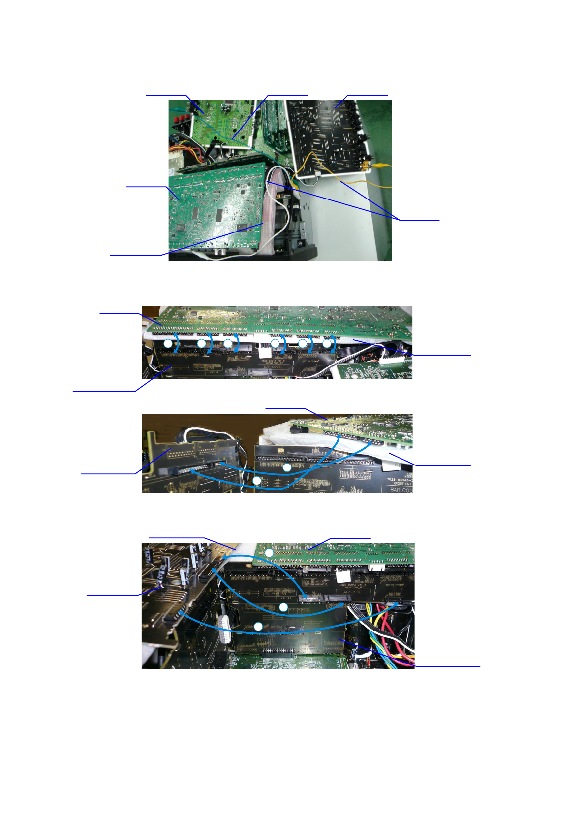
(3) PCB HDMI is detached from the chassis, and it puts it into the state turned inside out.
Please pave an insulation sheet that is larger than PCB HDMI under PCB.
Connect the ground point of PCB to the chassis with a ground lead or the like.
b
PCB INPUT PCB VIDEO
Ground lead
PCB HDMI
Insulation sheet
(4) Connect the four extension jig cables.
PCB HDMI
Ground lead
PCB FRONT CNT
PCB SIDE CNT
PCB VIDEO
Insulation sheet
PCB HDMI
2
9
11
34 5678
1
Insulation sheet
Insulation sheet
PCB HDMI
10
24
PCB FRONT CNT
PCB SIDE CNT
PCV FRONT CNT
13
14
15
16
Insulation sheet
12
PCB INPUT
Connection table of Board to Board
No. Pin Ref. No. PCB Ref. No. PCB
q
w
e
r
t
y
u
i
o
Q0
Q11
Q2
Q3
Q4
Q5
Q6
11 pin CP3 SIDE CNT
25 pin CP4 SIDE CNT
19 pin CP105 FRONT CNT
17 pin CP106 FRONT CNT
13 pin CP107 FRONT CNT
19 pin CP108 FRONT CNT N4913 HDMI
17 pin CP109 FRONT CNT
33 pin CP110 FRONT CNT
19 pin CP111 FRONT CNT N2001 VIDEO
17 pin CP112 FRONT CNT
13 pin CP113 FRONT CNT
13 pin CP114 FRONT CNT CX3001 INPUT
33 pin CP115 FRONT CNT
19 pin CP6 SIDE CNT
17 pin CP7 SIDE CNT
15 pin CP8 SIDE CNT CX3003 INPUT
N4908 HDMI
N4907 HDMI
N4910 HDMI
N4911 HDMI
N4912 HDMI
N4914 HDMI
N4916 HDMI
N2002 VIDEO
N2003 VIDEO
CN3000 INPUT
CX3000 INPUT
CX3002 INPUT
25
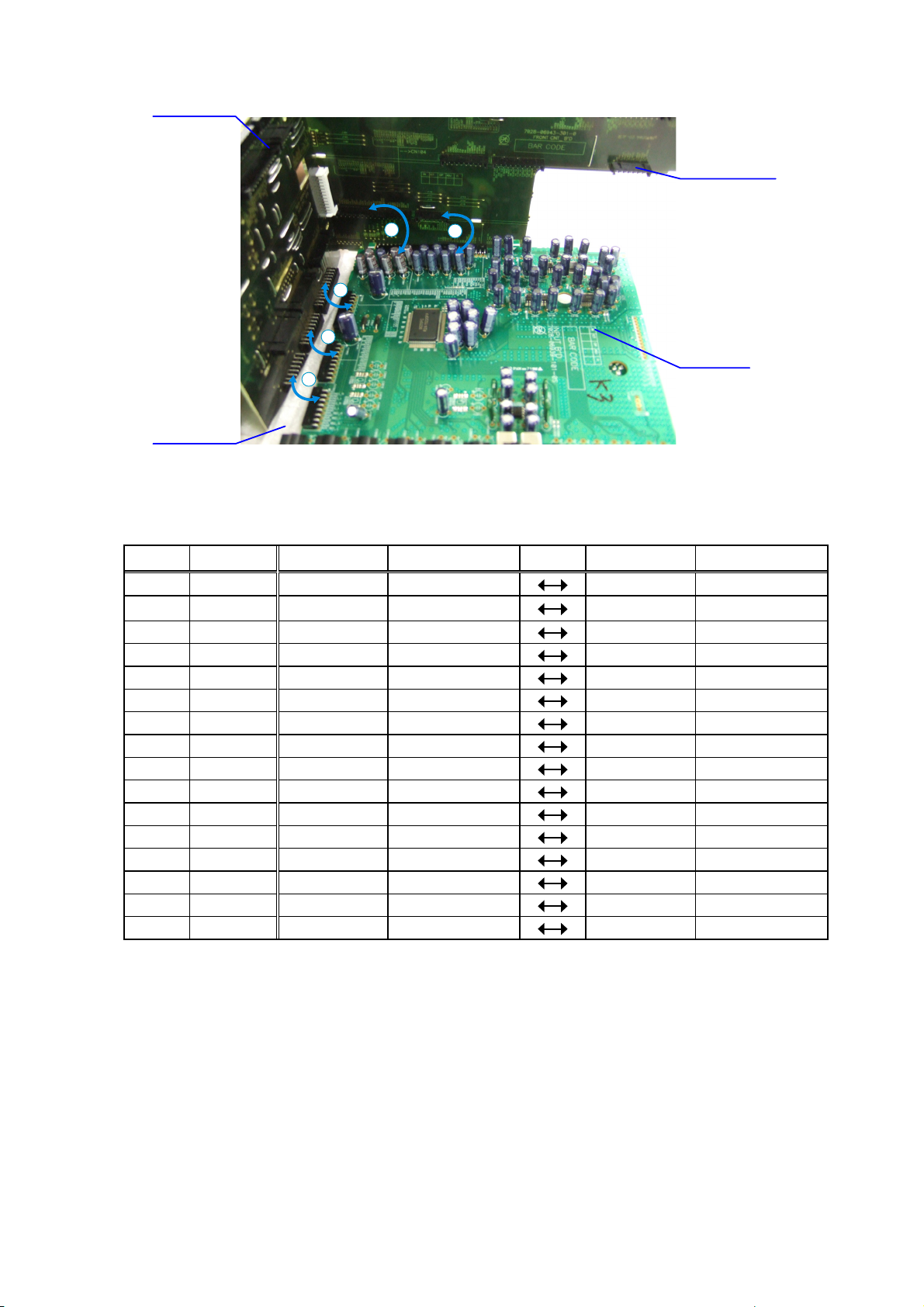
ABOUT REPLACE THE MICROPROCESSOR WITH A NEW ONE
When replaced of the U-PRO (Microprocessor) or the Flash ROM, confi rm contents of the following.
PWB Name Ref. No. Description
HDMI U5301 R5F64169DFD B SOFTWARE: Main
HDMI U5101 EN29LV160BB-70TIP B SOFTWARE: Main ROM
HDMI U5500 R5F3650KNFB B SOFTWARE: Sub
HDMI U3202 EN29LV160BB-70TIP B SOFTWARE: DSP ROM
HDMI U3000 EPM240T100C5N B SOFTWARE: Audio PLD
HDMI U1603 M25P40-VMN6PB B SOFTWARE: Video Confi g ROM
After
replaced
Remark
After replaced
A : Mask ROM (With software). No need write-in of software to the microprocessor.
B : Flash ROM (With software). Usually, no need write-in of software. But, when the software was updated, you should be
write-in of the new software to the microprocessor or fl ash ROM. Please check the software version.
C : Empty Flash ROM (Without software). You should be write-in of the software to the microprocessor or fl ash ROM.
Refer to "Update procedure" or "writing procedure", when you should be write-in the software.
VERSION UPGRADE PROCEDURE OF FIRMWARE
1. How to update by DPMS
You can update by downloading the latest fi rmware from the Internet.
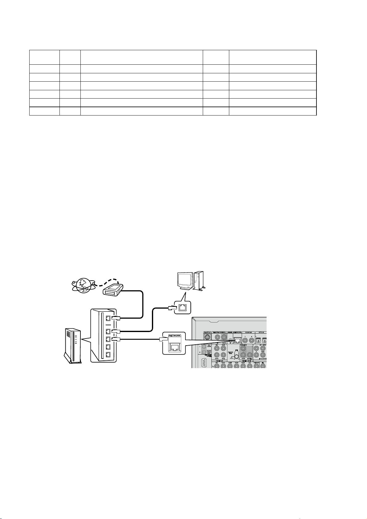
1.1. Connecting to the Network
(1) System Requirement
Internet Connection by Broadband Circuit
・
Modem
・
Router
・
Ethernet cable (CAT-5 or greater recommended)
・
(2) Setting
Internet
Computer
Router
Modem
To WAN port
To LAN port
To LAN port
ETHERNET
connector
LAN port/
Ethernet
connector
1.2. Check for Update and Update
Check if the latest fi rmware exists. You can also check approximately how long it will take to complete an update.
(1) Press the MENU button on the remote control to display the GUI menu.
(2) Use the cursor buttons to select "Manual Setup" → "Option Setup" → "Firmware Update" → "Update Check".
(3) Press the ENTER buttom.
The latest version of the fi rmware uploaded to the web is displayed.
・
If the latest fi rmware version is on the web, proceed to (4).
・
If the latest fi rmware is already installed, press the MENU button to close the menu.
・
(4) Use the cursor buttons to select "Update", then press the ENTER button.
During update, the power indicator lights red and the GUI screen is shut down. And a rough remaining time is
・
indicated on the display.
When updating is complete the power indicator turns off and normal status is resumed.
・
(5) Press the MENU button to close the menu.
26

--- Cautions on Firmware Update ---
In order to use these functions, you must have the correct system requirements and settings for a broadband Internet
・
connection.
Do not turn off the power until updating is completed.
・
Even with a broadband connection to the Internet, approximately about 1 hour is required for the updating procedure
to be completed.
Once updating starts, normal operations on the SR7005 cannot be performed until updating is completed. Also, setting
items of the GUI menu of SR7005 or setting items of the image adjustment may be initialized.
Make a note of the settings before updating, and set them again after updating.
1.3. About the error code
See the chart below for error codes, details of faults, and coping strategies when fi rmware updates are performed
through DPMS (D&M Product Management Server).
Error
Code
01
02
03
04
05
06
07
Details of Error code Display Coping strategies
Log-in to DPMS has failed.
Line, etc., is busy when logging into
DPMS.
Connection to DPMS failed.
Firmware fi le data was requested
but error message was received.
Firmware fi le data was requested
but it timed out.
Firmware fi le data was requested
but error message was received.
All fi rmware fi le data was requested
but it timed out.
Login failed
01
Server is busy
02
Connection fail
03
Connection fail
04
Connection fail
05
Connection fail
06
Connection fail
07
Reset and update again.
Carry out the update in an environment that
has little network load.
Carry out the update in an environment
that has little network load.
Check the network connection.
Carry out the update in an environment
that has little network load.
Check the network connection.
Carry out the update in an environment
that has little network load.
Check the network connection.
Carry out the update in an environment
that has little network load.
Check the network connection.
Carry out the update in an environment
that has little network load.
Check the network connection.
Carry out the update in an environment
that has little network load.
Main CPU fi rmware fi le data was
requested but error message was
08
received.
Main CPU fi rmware fi le data was
09
requested but it timed out.
Error (NG) message received when
0A
downloading Main CPU fi rmware.
Error (line congestion) message
received when downloading Main
0B
CPU fi rmware.
Error (connection failure) message
received when downloading Main
0C
CPU fi rmware.
Connection fail
08
Connection fail
09
Download fail
0A
Download fail
0B
Download fail
0C
27
Check the network connection.
Carry out the update in an environment
that has little network load.
Check the network connection.
Carry out the update in an environment
that has little network load.
Check the network connection.
Carry out the update in an environment
that has little network load.
Check the network connection.
Carry out the update in an environment
that has little network load.
Check the network connection.
Carry out the update in an environment
that has little network load.
Error
Code
0D
10
Details of Error code Display Coping strategies
Data acquisition failed (timed out)
when downloading Main CPU
fi rmware. Received Package
Version is wrong.
Main CPU failed to receive fi rmware
for rewriting sent from
DM860 (when timed out).
Connection fail
0D
Main ***min
Updating fail 10
Check the network connection.
Carry out the update in an environment
that has little network load.
Turn the power off then back on.
Updating starts automatically.
Main CPU failed to receive fi rmware
for rewriting sent from DM860 (when
11
an error )
There was invalid data in the
fi rmware for rewriting sent from
12
DM860 to Main CPU (when a
Check Sum error).
The deletion of block data failed
13
before rewriting Main CPU.
The rewriting of block data failed
14
when rewriting Main CPU.
The data verifi cation was invalid
15
after rewriting Main CPU.
Log-in to DPMS has failed when
rewriting fi rmware such as Sub
36
CPU, DSP, FPGA, and PLD.
Line, etc., is busy when logging
into DPMS when rewriting fi rmware
37
such as Sub CPU, DSP, FPGA, and
PLD.
Main ***min
Updating fail 11
Main ***min
Updating fail 12
Main ***min
Erase fail 13
Main ***min
Updating fail 14
Main ***min
UpdateCheckNG 15
Login failed
36
Server is busy
37
Turn the power off then back on.
Updating starts automatically.
Turn the power off then back on.
Updating starts automatically.
Turn the power off then back on.
Updating starts automatically.
Turn the power off then back on.
Updating starts automatically.
Turn the power off then back on.
Updating starts automatically.
Carry out the update in an environment
that has little network load.
Carry out the update in an environment
that has little network load.
Connection to DPMS failed when
rewriting fi rmware such as Sub
38
CPU, DSP, FPGA, and PLD.
Connection to DPMS timed out
when rewriting fi rmware such as
39
Sub CPU, DSP, FPGA, and PLD.
Error (NG) message received
when downloading fi rmware when
3A
rewriting Main CPU.
Error (line congestion) message
received when downloading
3B
fi rmware when rewriting Main CPU.
Error (connection failure) message
received when downloading
3C
fi rmware when rewriting Main CPU.
Log-in to DPMS has failed when
rewriting fi rmware such as Sub
50
CPU, DSP, FPGA, and PLD.
Line, etc., is busy when logging
into DPMS when rewriting fi rmware
51
such as Sub CPU, DSP, FPGA, and
PLD.
Connection fail
38
Connection fail
39
Download fail
3A
Download fail
3B
Download fail
3C
Sub ***min
Login failed 50
Sub ***min
Server is busy51
Check the network connection.
Carry out the update in an environment
that has little network load.
Check the network connection.
Carry out the update in an environment
that has little network load.
Turn the power off then back on.
Updating starts automatically.
Carry out the update in an environment
that has little network load.
Turn the power off then back on.
Updating starts automatically.
Carry out the update in an environment
that has little network load.
Turn the power off then back on.
Updating starts automatically.
Carry out the update in an environment
that has little network load.
Carry out the update in an environment
that has little network load.
Carry out the update in an environment
that has little network load.
28
Error
Code
Details of Error code Display Coping strategies
Connection to DPMS failed when
rewriting fi rmware such as Sub
52
CPU, DSP, FPGA, and PLD.
Error message received regarding
fi rmware data after logging in to
54
DPMS when rewriting fi rmware such
as Sub CPU, DSP, FPGA, and PLD.
When rewriting fi rmware such as Sub
CPU, DS
55
was made for fi rmware data after
logging in to DPMS, but it timed out.
Failure to download fi rmware after
logging in to DPMS when rewriting
56
fi rmware such as Sub CPU, DSP,
FPGA, and PLD.
Firmware download error received
(line congestion) after logging in to
57
DPMS when rewriting fi rmware such
as Sub CPU, DSP, FPGA, and PLD.
Firmware download error received
(connection failure) after logging in to
58
DPMS when rewriting fi rmware such
as Sub CPU, DSP, FPGA, and PLD.
NACK received when "C" command
sent to Sub CPU, DSP, FPGA, PLD
5A
etc.
P, FPGA,
and PLD, request
Sub ***min
ConnectionFail52
Sub ***min
Updating fail 54
Sub ***min
Updating fail 55
Sub ***min
Download fail 56
Sub ***min
Server is busy57
Sub ***min
ConnectionFail58
Sub ***min
ConnectionFail5A
Check the network connection.
Carry out the update in an environment
that has little network load.
Turn the power off then back on.
Updating starts automatically.
Carry out the update in an environment
that has little network load.
Turn the power off then back on.
Updating starts automatically.
Carry out the update in an environment
that has little network load.
Turn the power off then back on.
Updating starts automatically.
Carry out the update in an environment
that has little network load.
Turn the power off then back on.
Updating starts automatically.
Carry out the update in an environment
that has little network load.
Turn the power off then back on.
Updating starts automatically.
Carry out the update in an environment
that has little network load.
Turn the power off then back on.
Updating starts automatically.
NACK received when "L" command
sent to Sub CPU, DSP, FPGA, PLD
5B
etc.
Sub CPU, DSP, FPGA, PLD etc.
failed to receive fi rmware for
5C
rewriting sent from DM860 (when
timed out).
Sub CPU, DSP, FPGA, PLD etc.
failed to receive fi rmware for
5D
rewriting sent from DM860 (when
an error).
Invalid data in fi rmware such as
Sub CPU, DSP, FPGA, and PLD for
5E
rewriting sent from DM860 (when a
Check Sum error).
Invalid data in fi rmware such as
Sub CPU, DSP, FPGA, and PLD for
5F
rewriting sent from DM860 (invalid
data received).
NACK received when "P" command
sent to Sub CPU, DSP, FPGA, PLD
60
etc.
NACK received when "I" command
sent to Sub CPU, DSP, FPGA, PLD
61
etc.
Sub ***min
Updating fail 5B
Sub ***min
Updating fail 5C
Sub ***min
Updating fail 5D
Sub ***min
Updating fail 5E
Sub ***min
Updating fail 5F
Sub ***min
Updating fail 60
Sub ***min
UpdateCheckNG 61
Turn the power off then back on.
Updating starts automatically.
Turn the power off then back on.
Updating starts automatically.
Turn the power off then back on.
Updating starts automatically.
Turn the power off then back on.
Updating starts automatically.
Turn the power off then back on.
Updating starts automatically.
Turn the power off then back on.
Updating starts automatically.
Turn the power off then back on.
Updating starts automatically.
Start failure of Sub μ-com.
62
Failure to acquire serial fl ash data
80
and before deleting serial fl ash.
Sub ***min
Updating fail 62
OSD ***min
Updating fail 80
29
Turn the power off then back on. Updating
starts automatically.
Turn the power off then back on.
Updating starts automatically.

Error
Code
Details of Error code Display Coping strategies
Failure to delete data before
81
rewriting serial fl ash.
Failure to receive fi rmware for serial
fl ash rewriting sent by DM860 (when
82
timed out).
Failure to receive fi rmware for serial
fl ash rewriting sent by DM860 (when
83
an error).
Failure to receive fi rmware for serial
fl ash rewriting sent by DM860 (when
84
a Check Sum error).
Failure to receive fi rmware for serial
fl ash rewriting sent by DM860 (when
85
invalid data received).
Failure to rewrite when writing data
86
in serial fl ash.
Failure to acquire (Application
Mode) IP address before rewriting
A0
DM860 (AutoIP).
OSD ***min
Updating fail 81
OSD ***min
Updating fail 82
OSD ***min
Updating fail 83
OSD ***min
Updating fail 84
OSD ***min
Updating fail 85
OSD ***min
Updating fail 86
Ether IMG ***min
ConnectionFailA0
Turn the power off then back on.
Updating starts automatically.
Turn the power off then back on.
Updating starts automatically.
Turn the power off then back on.
Updating starts automatically.
Turn the power off then back on.
Updating starts automatically.
Turn the power off then back on.
Updating starts automatically.
Turn the power off then back on.
Updating starts automatically.
Check the network connection.
Carry out the update in an environment
that has little network load.
Failure to acquire (Application
Mode) IP address before rewriting
A1
DM860 (when timed out).
Notifi cation of invalid login via DPMS
access when rewriting DM860
A2
related fi rmware (Application Mode).
Notifi cation of line congestion
via DPMS access when rewriting
A3
DM860 related fi rmware (Application
Mode).
Notifi cation of connection failure
via DPMS access when rewriting
A4
DM860 related fi rmware (Application
Mode).
Firmware data error message
received after DPMS login when
A6
rewriting DM860 related fi rmware
(Application Mode).
When rewriting DM860 related
fi rmware (Application Mode),
A7
request was made for fi rmware data
after DPMS login but it timed out.
Failure to acquire (Boot Loader
Mode) IP address before rewriting
A8
DM860 (AutoIP).
Ether IMG ***min
ConnectionFailA1
Ether IMG ***min
Login failed A2
Ether IMG ***min
Server is busyA3
Ether IMG ***min
ConnectionFailA4
Ether IMG ***min
Updating fail A6
Ether IMG ***min
Updating fail A7
Ether IMG ***min
ConnectionFailA8
Check the network connection.
Carry out the update in an environment
that has little network load.
Check the network connection.
Carry out the update in an environment
that has little network load.
Check the network connection.
Carry out the update in an environment
that has little network load.
Check the network connection.
Carry out the update in an environment
that has little network load.
Turn the power off then back on.
Updating starts automatically.
Carry out the update in an environment
that has little network load.
Turn the power off then back on.
Updating starts automatically.
Carry out the update in an environment
that has little network load.
Check the network connection.
Carry out the update in an environment
that has little network load.
Failure to acquire (Boot Loader
Mode) IP address before rewriting
A9
DM860 (when timed out).
Notifi cation of invalid login via
DPMS access when rewriting
AA
DM860 related fi rmware (Boot
Loader Mode).
Ether IMG ***min
ConnectionFailA9
Ether IMG ***min
Login failed AA
30
Check the network connection.
Carry out the update in an environment
that has little network load.
Check the network connection.
Carry out the update in an environment
that has little network load.
 Loading...