

Page 1

MODEL: NB3540 (NB3540, S34A2-D)SERVICE MANUAL
Internal Use Only
Website http://biz.lgservice.com
Sound Bar System
SERVICE MANUAL
MODEL: NB3540
P/NO : AFN76793810 AUGUST, 2014
CAUTION
BEFORE SERVICING THE UNIT, READ THE “SAFETY PRECAUTIONS”
IN THIS MANUAL.
(NB3540, S34A2-D)
Page 2

CONTENTS
SECTION 1 ........ GENERAL
SECTION 2 ........ CABINET & MAIN CHASSIS
SECTION 3 ........ ELECTRICAL
SECTION 4 ........ REPLACEMENT PARTS LIST
1-1
Page 3

SECTION 1
GENERAL
CONTENTS
ESD PRECAUTIONS ....................................................................................................................................... 1-3
HIDDEN KEY MODE ........................................................................................................................................ 1-4
SOFTWARE UPDATE METHOD .................................................................................................................... 1-5
SERVICE INFORMATION FOR EEPROM .................................................................................................... 1-6
SPECIFICATIONS ............................................................................................................................................ 1-7
1-2
Page 4

ESD PRECAUTIONS
Electrostatically Sensitive Devices (ESD)
Some semiconductor (solid state) devices can be damaged easily by static electricity. Such components
commonly are called Electrostatically Sensitive Devices (ESD). Examples of typical ESD devices are integrated
circuits and some field-effect transistors and semiconductor chip components. The following techniques should
be used to help reduce the incidence of component damage caused by static electricity.
1. Immediately before handling any semiconductor component or semiconductor-equipped assembly, drain off
any electrostatic charge on your body by touching a known earth ground. Alternatively, obtain and wear a
commercially available discharging wrist strap device, which should be removed for potential shock reasons
prior to applying power to the unit under test.
2. After removing an electrical assembly equipped with ESD devices, place the assembly on a conductive surface
such as aluminum foil, to prevent electrostatic charge buildup or exposure of the assembly.
3. Use only a grounded-tip soldering iron to solder or unsolder ESD devices.
4. Use only an anti-static solder removal device. Some solder removal devices not classified as "anti-static" can
generate electrical charges sufficient to damage ESD devices.
5. Do not use freon-propelled chemicals. These can generate electrical charges sufficient to damage ESD
devices.
6. Do not remove a replacement ESD device from its protective package until immediately before you are
ready to install it. (Most replacement ESD devices are packaged with leads electrically shorted together by
conductive foam, aluminum foil or comparable conductive materials).
7. Immediately before removing the protective material from the leads of a replacement ESD device, touch the
protective material to the chassis or circuit assembly into which the device will by installed.
CAUTION : BE SURE NO POWER IS APPLIED TO THE CHASSIS OR CIRCUIT, AND OBSERVE ALL OTHER
SAFETY PRECAUTIONS.
8. Minimize bodily motions when handing unpackaged replacement ESD devices. (Otherwise harmless motion
such as the brushing together of your clothes fabric or the lifting of your foot from a carpeted floor can generate
static electricity sufficient to damage an ESD device).
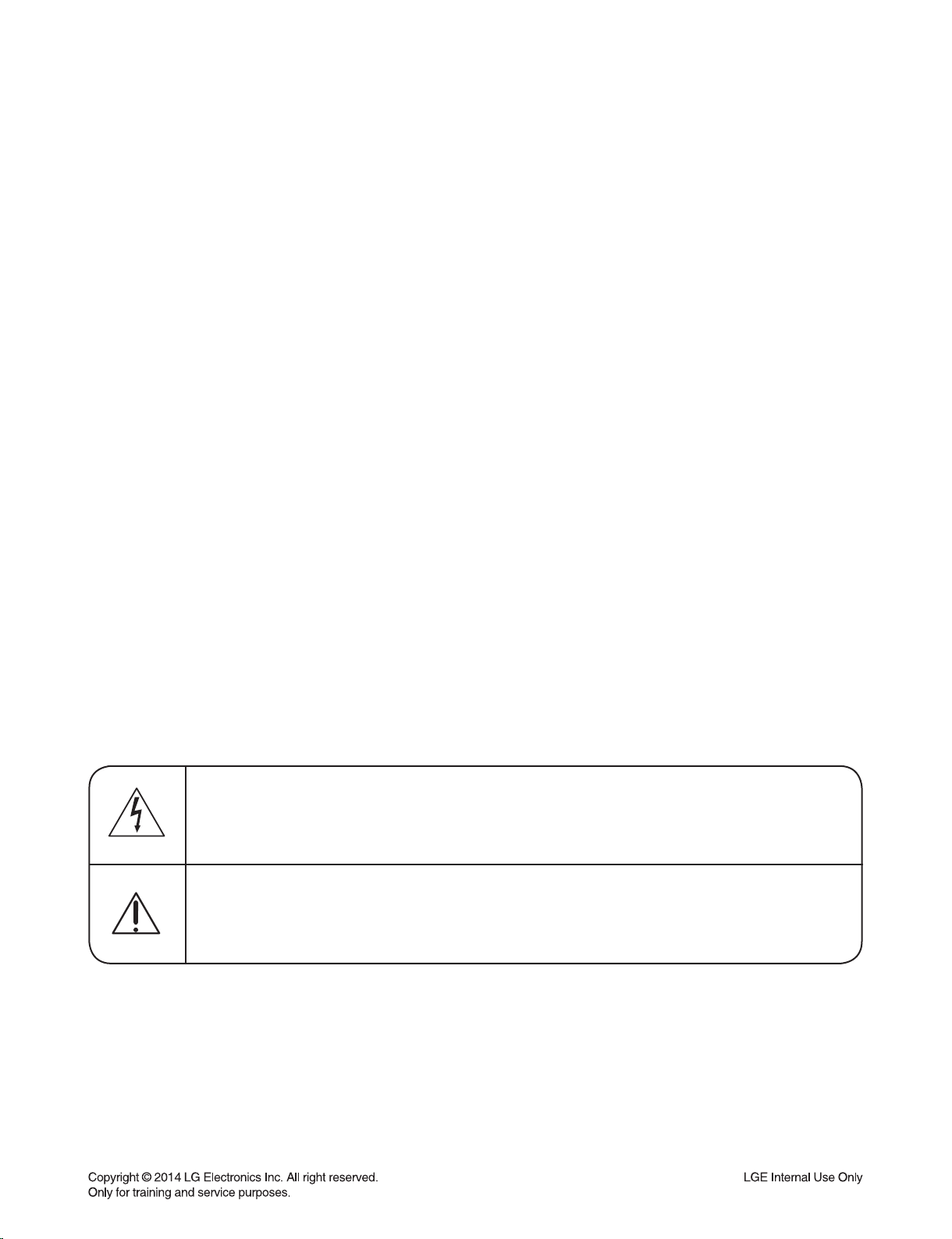
CAUTION. GRAPHIC SYMBOLS
THE LIGHTNING FLASH WITH APROWHEAD SYMBOL. WITHIN AN EQUILATERAL TRIANGLE, IS
INTENDED TO ALERT THE SERVICE PERSONNEL TO THE PRESENCE OF UNINSULATED
“DANGEROUS VOLTAGE” THAT MAY BE OF SUFFICIENT MAGNITUDE TO CONSTITUTE A RISK OF
ELECTRIC SHOCK.
THE EXCLAMATION POINT WITHIN AN EQUILATERAL TRIANGLE IS INTENDED TO ALERT THE
SERVICE PERSONNEL TO THE PRESENCE OF IMPORTANT SAFETY INFORMATION IN SERVICE
LITERATURE.
1-3
Page 5

HIDDEN KEY MODE
• Status: Power ON
HIDDEN MODE ENTRANCE KEY EXIT KEY DISPLAY RESULT
1) ESS(DSP)
2) Touch Key
3) Wireless SPK
module TX
4) Wireless SPK
module RX
5) EQ
6) EEPROM option
value (on Scroll)
Version Check
EEPROM INITIAL
EEPROM EDIT
Wireless Factory
Reset
Wireless SPK RF
change
Clip Off
Monitoring
Changed Gain
at Clip ON
CLIP Algorithm Edit
MAX Volume Edit
APD On/Off
Front 'Vol-' + RMC
Play for 3sec
Front 'Vol-' + RMC '0'
for 3sec
Front 'Vol-' + RMC '2'
for 3sec
Set volume "VOL MIN"
+ RMC 'mute' for 3sec
Front 'Vol-' + RMC '4'
for 3sec
Front 'Vol-' + RMC '8'
for 3sec
Front 'Vol-' + RMC '8'
for 3sec
Front 'Vol-' + RMC '9'
for 3sec
Front Stop + RMC
'Sleep' for 3sec
Front 'Vol-' + RMC '3'
for 3sec
E1311050
T1311050
POWER OFF
auto exit "E2P CLEAR" EEPROM initializing
Toggling "OP0-10" Edit Micom option
- "W RESET" -
-- -
Toggling "CLIP OFF" -
Toggling 00 00 -
-- -
Toggling MVOL-XX -
Toggling APD ON / APD OFF APD ON/OFF
TX 053
RX 156
Q1311050
01 E1 00 30 11
1-4
Page 6

SOFTWARE UPDATE METHOD
USB update for NB5540/4540/3540
DSP_NB5540.rom is an update fi le for NB5540 Main/DSP software.
DSP_NB4540.rom is an update fi le for NB4540 Main/DSP software.
DSP_NB3540.rom is an update fi le for NB3540 Main/DSP software.
EQ_PRG_NB5540.bin is an update fi le for NB5540 EQ software.
EQ_PRG_NB4540.bin is an update fi le for NB4540 EQ software.
EQ_PRG_NB3540.bin is an update fi le for NB3540 EQ Software.
WIRELESS_TX.bin is an update fi le for Wireless TX(MAIN SET) software.
WIRELESS_RX.bin is an update fi le for Wireless TX(Woofer) software.
Step 1 : Creating a Firmware Update Device
You can create a fi rmware update fi les on your USB memory device(FAT32).
To create a fi rmware update in a USB memory device, copy the update fi le to the USB device.
Preparation:
1. Insert a USB memory device into the PC.
2. Copy the latest version of fi rmware update fi les to the USB drive.
(You do not need to create directory, the fi les will be saved in the root directory.)
3. It is impossible to multiple update at same time. (It can’t select update fi le. But, it has an update priority.
An update priority is as follows. <DSP, Wireless RX, Wireless TX, EQ>)
The USB memory device should have at least 2 MB of free space to save the fi rmware update fi les.
Step 2 : Updating the speaker bar(NB5540/4540/3540)
If you copy a update fi le to an USB memory, you can update.
1. Turn on the speaker bar and move to USB function.
2. Insert USB memory that contains the update fi le of the latest fi rmware version into the speaker bar.
- Insert the USB memory device to the USB port of the speaker bar.
3-1. If you insert an USB memory that contains the DSP update fi le, it displays “DSP UP” on FLD.
And it starts DSP update. Updating DSP Software will take about 1 minutes.
3-2. If you insert an USB memory that contains the EQ update fi le, it displays “EQ UP” on FLD.
And it starts EQ update. Updating EQ Software will take about 3 ~ 5 sec.
3-3. If you insert an USB memory that contains the WIRELESS TX update fi le, it displays “UPDATE” on FLD.
WR“00”indicates a progress percentage. And it starts Wireless TX update.
Updating Wireless TX Software will take about 2 minutes.
3-4. If you insert an USB memory that contains the WIRELESS RX update fi le, it displays “UPDATE” on FLD.
SEND “00” indicates a progress percentage. And it starts Wireless RX update.
Updating Wireless RX Software will take about 2 minutes.
CAUTION : Do not turn off the power during fi rmware update.
4. After update, it turns off power automatically.
5. Disconnect the power cord of the main unit and the wireless subwoofer.
and connect them again after the LED of the main unit and the wireless subwoofer is fully turned off.
6. The system now operates with the new version.
1-5
Page 7

SERVICE INFORMATION FOR EEPROM
• FACTORY RESET: SET(“VOL-” KEY) + REMOCON “2”
[ AUDIO MICOM OPTION CODE SETTING ]
SET(“VOL-” KEY) + REMOCON “2” (MORE THAN 5 SECONDS) Ö CHANGE OPTION CODE WITH THE
ARROW KEY (REPEAT, PLAY/PAUSE, SKIP KEY) AND PRESS REMOCON STOP KEY Ö SET(“VOL-” KEY)
+ REMOCON “2” Ö COMPLETED.
1-6
Page 8

SPECIFICATIONS
• GENERAL (NB3540)
AC adapter requirements 100 - 240 V ~ 50 / 60 Hz, 25 V 2 A
Power consumption 27 W
Dimensions (W x H x D) (770 x 35 x 75) mm
Net Weight (Approx.) 1.3 kg
Operating temperature 5 °C to 35 °C (41 °F to 95 °F)
Operating humidity 5 % to 90 %
• INPUT/OUTPUT
OPTICAL IN 3 V (p-p), Optical jack x 1
PORT. IN 0.5 Vrms (3.5 mm stereo jack) x 1
Available Digital Input Audio Sampling Frequency 32 kHz, 44.1 kHz, 48 kHz, 96 kHz
• USB
Version 1.1
Bus Power Supply 5 V 500 mA
• AMPLIFIER
Total 320 W
Front 80 W x 2 (4 Ω at 1 kHz)
Subwoofer 160 W (3 Ω at 80 Hz)
THD 10 %
• WIRELESS SUBWOOFER (S34A2-D)
Power requirements 100 - 240 V ~ 50 / 60 Hz
Power consumption 40 W
Type 1 Way 1 Speaker
Impedance 3 Ω
Rated Input Power 160 W
Max. Input Power 320 W
Dimensions (W x H x D) (170 x 360 x 316) mm
Net Weight (Approx.) 5.55 kg
Ø Designs and specifications are subject to change without prior notice.
1-7
Page 9

MEMO
1-8
Page 10

SECTION 2
CABINET & MAIN CHASSIS
CONTENTS
EXPLODED VIEWS ......................................................................................................................................... 2-3
1. RECEIVER BAR SECTION (NB3540) ...................................................................................................... 2-3
2. WIRELESS SUBWOOFER SECTION (S34A2-D) .................................................................................... 2-5
3. PACKING ACCESSORY SECTION ......................................................................................................... 2-7
2-1
Page 11

MEMO
2-2
Page 12

CONTENTS
SECTION 1 ........ GENERAL
SECTION 2 ........ CABINET & MAIN CHASSIS
SECTION 3 ........ ELECTRICAL
SECTION 4 ........ REPLACEMENT PARTS LIST
1-1
Page 13

SECTION 1
GENERAL
CONTENTS
ESD PRECAUTIONS ....................................................................................................................................... 1-3
HIDDEN KEY MODE ........................................................................................................................................ 1-4
SOFTWARE UPDATE METHOD .................................................................................................................... 1-5
SERVICE INFORMATION FOR EEPROM .................................................................................................... 1-6
SPECIFICATIONS ............................................................................................................................................ 1-7
1-2
Page 14
ESD PRECAUTIONS
Electrostatically Sensitive Devices (ESD)
Some semiconductor (solid state) devices can be damaged easily by static electricity. Such components
commonly are called Electrostatically Sensitive Devices (ESD). Examples of typical ESD devices are integrated
circuits and some field-effect transistors and semiconductor chip components. The following techniques should
be used to help reduce the incidence of component damage caused by static electricity.
1. Immediately before handling any semiconductor component or semiconductor-equipped assembly, drain off
any electrostatic charge on your body by touching a known earth ground. Alternatively, obtain and wear a
commercially available discharging wrist strap device, which should be removed for potential shock reasons
prior to applying power to the unit under test.
2. After removing an electrical assembly equipped with ESD devices, place the assembly on a conductive surface
such as aluminum foil, to prevent electrostatic charge buildup or exposure of the assembly.
3. Use only a grounded-tip soldering iron to solder or unsolder ESD devices.
4. Use only an anti-static solder removal device. Some solder removal devices not classified as "anti-static" can
generate electrical charges sufficient to damage ESD devices.
5. Do not use freon-propelled chemicals. These can generate electrical charges sufficient to damage ESD
devices.
6. Do not remove a replacement ESD device from its protective package until immediately before you are
ready to install it. (Most replacement ESD devices are packaged with leads electrically shorted together by
conductive foam, aluminum foil or comparable conductive materials).
7. Immediately before removing the protective material from the leads of a replacement ESD device, touch the
protective material to the chassis or circuit assembly into which the device will by installed.
CAUTION : BE SURE NO POWER IS APPLIED TO THE CHASSIS OR CIRCUIT, AND OBSERVE ALL OTHER
SAFETY PRECAUTIONS.
8. Minimize bodily motions when handing unpackaged replacement ESD devices. (Otherwise harmless motion
such as the brushing together of your clothes fabric or the lifting of your foot from a carpeted floor can generate
static electricity sufficient to damage an ESD device).
CAUTION. GRAPHIC SYMBOLS
THE LIGHTNING FLASH WITH APROWHEAD SYMBOL. WITHIN AN EQUILATERAL TRIANGLE, IS
INTENDED TO ALERT THE SERVICE PERSONNEL TO THE PRESENCE OF UNINSULATED
“DANGEROUS VOLTAGE” THAT MAY BE OF SUFFICIENT MAGNITUDE TO CONSTITUTE A RISK OF
ELECTRIC SHOCK.
THE EXCLAMATION POINT WITHIN AN EQUILATERAL TRIANGLE IS INTENDED TO ALERT THE
SERVICE PERSONNEL TO THE PRESENCE OF IMPORTANT SAFETY INFORMATION IN SERVICE
LITERATURE.
1-3
Page 15

HIDDEN KEY MODE
• Status: Power ON
HIDDEN MODE ENTRANCE KEY EXIT KEY DISPLAY RESULT
1) ESS(DSP)
2) Touch Key
3) Wireless SPK
module TX
4) Wireless SPK
module RX
5) EQ
6) EEPROM option
value (on Scroll)
Version Check
EEPROM INITIAL
EEPROM EDIT
Wireless Factory
Reset
Wireless SPK RF
change
Clip Off
Monitoring
Changed Gain
at Clip ON
CLIP Algorithm Edit
MAX Volume Edit
APD On/Off
Front 'Vol-' + RMC
Play for 3sec
Front 'Vol-' + RMC '0'
for 3sec
Front 'Vol-' + RMC '2'
for 3sec
Set volume "VOL MIN"
+ RMC 'mute' for 3sec
Front 'Vol-' + RMC '4'
for 3sec
Front 'Vol-' + RMC '8'
for 3sec
Front 'Vol-' + RMC '8'
for 3sec
Front 'Vol-' + RMC '9'
for 3sec
Front Stop + RMC
'Sleep' for 3sec
Front 'Vol-' + RMC '3'
for 3sec
E1311050
T1311050
POWER OFF
auto exit "E2P CLEAR" EEPROM initializing
Toggling "OP0-10" Edit Micom option
- "W RESET" -
-- -
Toggling "CLIP OFF" -
Toggling 00 00 -
-- -
Toggling MVOL-XX -
Toggling APD ON / APD OFF APD ON/OFF
TX 053
RX 156
Q1311050
01 E1 00 30 11
1-4
Page 16

SOFTWARE UPDATE METHOD
USB update for NB5540/4540/3540
DSP_NB5540.rom is an update fi le for NB5540 Main/DSP software.
DSP_NB4540.rom is an update fi le for NB4540 Main/DSP software.
DSP_NB3540.rom is an update fi le for NB3540 Main/DSP software.
EQ_PRG_NB5540.bin is an update fi le for NB5540 EQ software.
EQ_PRG_NB4540.bin is an update fi le for NB4540 EQ software.
EQ_PRG_NB3540.bin is an update fi le for NB3540 EQ Software.
WIRELESS_TX.bin is an update fi le for Wireless TX(MAIN SET) software.
WIRELESS_RX.bin is an update fi le for Wireless TX(Woofer) software.
Step 1 : Creating a Firmware Update Device
You can create a fi rmware update fi les on your USB memory device(FAT32).
To create a fi rmware update in a USB memory device, copy the update fi le to the USB device.
Preparation:
1. Insert a USB memory device into the PC.
2. Copy the latest version of fi rmware update fi les to the USB drive.
(You do not need to create directory, the fi les will be saved in the root directory.)
3. It is impossible to multiple update at same time. (It can’t select update fi le. But, it has an update priority.
An update priority is as follows. <DSP, Wireless RX, Wireless TX, EQ>)
The USB memory device should have at least 2 MB of free space to save the fi rmware update fi les.
Step 2 : Updating the speaker bar(NB5540/4540/3540)
If you copy a update fi le to an USB memory, you can update.
1. Turn on the speaker bar and move to USB function.
2. Insert USB memory that contains the update fi le of the latest fi rmware version into the speaker bar.
- Insert the USB memory device to the USB port of the speaker bar.
3-1. If you insert an USB memory that contains the DSP update fi le, it displays “DSP UP” on FLD.
And it starts DSP update. Updating DSP Software will take about 1 minutes.
3-2. If you insert an USB memory that contains the EQ update fi le, it displays “EQ UP” on FLD.
And it starts EQ update. Updating EQ Software will take about 3 ~ 5 sec.
3-3. If you insert an USB memory that contains the WIRELESS TX update fi le, it displays “UPDATE” on FLD.
WR“00”indicates a progress percentage. And it starts Wireless TX update.
Updating Wireless TX Software will take about 2 minutes.
3-4. If you insert an USB memory that contains the WIRELESS RX update fi le, it displays “UPDATE” on FLD.
SEND “00” indicates a progress percentage. And it starts Wireless RX update.
Updating Wireless RX Software will take about 2 minutes.
CAUTION : Do not turn off the power during fi rmware update.
4. After update, it turns off power automatically.
5. Disconnect the power cord of the main unit and the wireless subwoofer.
and connect them again after the LED of the main unit and the wireless subwoofer is fully turned off.
6. The system now operates with the new version.
1-5
Page 17

SERVICE INFORMATION FOR EEPROM
• FACTORY RESET: SET(“VOL-” KEY) + REMOCON “2”
[ AUDIO MICOM OPTION CODE SETTING ]
SET(“VOL-” KEY) + REMOCON “2” (MORE THAN 5 SECONDS) Ö CHANGE OPTION CODE WITH THE
ARROW KEY (REPEAT, PLAY/PAUSE, SKIP KEY) AND PRESS REMOCON STOP KEY Ö SET(“VOL-” KEY)
+ REMOCON “2” Ö COMPLETED.
1-6
Page 18

SPECIFICATIONS
• GENERAL (NB3540)
AC adapter requirements 100 - 240 V ~ 50 / 60 Hz, 25 V 2 A
Power consumption 27 W
Dimensions (W x H x D) (770 x 35 x 75) mm
Net Weight (Approx.) 1.3 kg
Operating temperature 5 °C to 35 °C (41 °F to 95 °F)
Operating humidity 5 % to 90 %
• INPUT/OUTPUT
OPTICAL IN 3 V (p-p), Optical jack x 1
PORT. IN 0.5 Vrms (3.5 mm stereo jack) x 1
Available Digital Input Audio Sampling Frequency 32 kHz, 44.1 kHz, 48 kHz, 96 kHz
• USB
Version 1.1
Bus Power Supply 5 V 500 mA
• AMPLIFIER
Total 320 W
Front 80 W x 2 (4 Ω at 1 kHz)
Subwoofer 160 W (3 Ω at 80 Hz)
THD 10 %
• WIRELESS SUBWOOFER (S34A2-D)
Power requirements 100 - 240 V ~ 50 / 60 Hz
Power consumption 40 W
Type 1 Way 1 Speaker
Impedance 3 Ω
Rated Input Power 160 W
Max. Input Power 320 W
Dimensions (W x H x D) (170 x 360 x 316) mm
Net Weight (Approx.) 5.55 kg
Ø Designs and specifications are subject to change without prior notice.
1-7
Page 19

MEMO
1-8
Page 20

SECTION 2
CABINET & MAIN CHASSIS
CONTENTS
EXPLODED VIEWS ......................................................................................................................................... 2-3
1. RECEIVER BAR SECTION (NB3540) ...................................................................................................... 2-3
2. WIRELESS SUBWOOFER SECTION (S34A2-D) .................................................................................... 2-5
3. PACKING ACCESSORY SECTION ......................................................................................................... 2-7
2-1
Page 21

MEMO
2-2
Page 22

E
D
C
A
H
B
E
D
G
H
C
A
B
G
F
F
256
A44B
A44C
A44A
258
258
263
258
258
457
457
464
251
A46
A42
A43
464
464
464
464
A52
A55
261
262
260
263
464
A54
457
CABLE5
CABLE1
CABLE2
CABLE7
CABLE3
FRONT
WIRELESS
B/T
KEY
259
EXPLODED VIEWS
1. RECEIVER BAR SECTION (NB3540)
Page 23

B
C
E
B
C
D
D
SMPS
953
F
E
WIRELESS
955
953
953
951
953
953
AMP
A47W
A
A
952
954
954
954
954
A54W
A45W
A900
KEY
F
300W
2. WIRELESS SUBWOOFER SECTION (S34A2-D)
NOTES) THE EXCLAMATION POINT WITHIN AN
EQUILATERAL TRIANGLE IS INTENDED
TO ALERT THE SERVICE PERSONNEL
TO THE PRESENCE OF IMPORTANT
SAFETY INFORMATION IN SERVICE
LITERATURE.
Page 24

511 Screws (2)
300 Po wer cord
806 Op tical Cable
900 Remote control
3. PACKING ACCESSORY SECTION
801 Owner’s manual
820A USB gender
833 AC adapter
808 Batteries
829 Cable ties (2)
835 Wall bracket (2)
803 Packing
802 Box
804 Bag
803 Packing
Page 25

MEMO
2-8
Page 26

SECTION 3
ELECTRICAL
CONTENTS
ONE POINT REPAIR GUIDE .......................................................................................................................... 3-2
1. NO POWER PROBLEM (25 VA) ............................................................................................................ 3-2
2. POWER ON ERROR .............................................................................................................................. 3-3
3. NO SOUND (PORTABLE FUNCTION) .................................................................................................. 3-5
4. NO WIRELESS ....................................................................................................................................... 3-6
5. NO BLUETOOTH .................................................................................................................................... 3-7
6. NO SOUND (USB) .................................................................................................................................. 3-8
7. NO SOUND (OPTICAL) .......................................................................................................................... 3-9
WAVEFORMS OF MAJOR CHECK POINT ................................................................................................ 3-10
1. SYSTEM PART-1 (X-TAL) .................................................................................................................... 3-10
2. SYSTEM PART-2 (FLASH) .................................................................................................................. 3-11
3. SYSTEM PART-3 (EEPROM) .............................................................................................................. 3-12
4. SYSTEM PART-4 (USB) ....................................................................................................................... 3-13
5. SYSTEM PART-5 (TACT KEY) ............................................................................................................ 3-14
6. SYSTEM PART-6 (REMOCON) ........................................................................................................... 3-16
7. SYSTEM PART-7 (OPTICAL) ............................................................................................................... 3-17
WIRING DIAGRAM ........................................................................................................................................ 3-19
BLOCK DIAGRAM ......................................................................................................................................... 3-21
CIRCUIT DIAGRAMS .................................................................................................................................... 3-23
1. MAIN - DSP CIRCUIT DIAGRAM ......................................................................................................... 3-23
2. MAIN - AMP CIRCUIT DIAGRAM......................................................................................................... 3-25
3. MAIN - POWER CIRCUIT DIAGRAM ................................................................................................... 3-27
4. FRONT CIRCUIT DIAGRAM ................................................................................................................ 3-29
5. TACT KEY CIRCUIT DIAGRAM ........................................................................................................... 3-31
6. WOOFER SMPS CIRCUIT DIAGRAM ................................................................................................. 3-33
7. WOOFER AMP CIRCUIT DIAGRAM .................................................................................................... 3-35
8. WOOFER KEY CIRCUIT DIAGRAM .................................................................................................... 3-37
CIRCUIT VOLTAGE CHART ........................................................................................................................ 3-39
PRINTED CIRCUIT BOARD DIAGRAMS .................................................................................................... 3-43
1. MAIN P. C. BOARD .............................................................................................................................. 3-43
2. FRONT P. C. BOARD ........................................................................................................................... 3-45
3. TACT KEY P. C. BOARD ..................................................................................................................... 3-45
4. WOOFER SMPS P. C. BOARD ............................................................................................................ 3-47
5. WOOFER AMP P. C. BOARD .............................................................................................................. 3-49
6. WOOFER KEY P. C. BOARD ............................................................................................................... 3-51
7. WOOFER LED P. C. BOARD ............................................................................................................... 3-51
3-1
Page 27

ONE POINT REPAIR GUIDE
1. NO POWER PROBLEM (25 VA)
No power problem occurs when you power on the unit
1-1. Solution
Replace the fuse F600 or F601.
1-2. How to troubleshoot (Countermeasure)
1) Change adaptor, replace F601, F602, L632.
1-3. Service hint (Any picture / Remark)
< Main board top view >
3-2
Page 28

ONE POINT REPAIR GUIDE
2. POWER ON ERROR
No display or Not working.
2-1. IC600
1) Check 3.7 VA at L603.
2) If 3.7 VA is not output, check 25 VA at No.7 Pin of IC600.
3) 1), 2) is OK. Replace IC600.
L603
IC600
< Main board top view >
2-2. IC505
1) Check 3.3 VA at L514.
2) If 3.3 VA is not output, check 3.7 VA at No.1 & 2 Pin of IC505.
3) 1), 2) is OK. Replace IC505.
IC505
L514
< Main board bottom view >
3-3
Page 29

ONE POINT REPAIR GUIDE
2-3. IC605
1) Check 3.3 VA at R644.
2) If 3.3 VA is not output, check 3.7 VA at No.1 Pin of IC605.
3) 1), 2) is OK. Replace IC605.
R644
IC605
< Main board bottom view >
2-4. IC606
1) Check 3.3 VA at L610.
2) If 3.3 VA is not output, check 3.7 VA at No.1 Pin of IC606.
3) 1), 2) is OK. Replace IC608.
L610
IC606
< Main board top view >
3-4
Page 30

ONE POINT REPAIR GUIDE
3. NO SOUND (PORTABLE FUNCTION)
3-1. Solution
Replace IC502 or Portable Jack.
3-2. How to troubleshoot (Countermeasure)
1) Please check the soldering status of portable jack(JK500).
2) Please check pin2, 3(portable L/R signal) of portable jack(JK500).
If you cannot find input signal, replace portable jack(JK500).
3) If you can find input signal, check pin122,123 of IC502.
If you cannot find signal of pin122, 123, re-soldering peripheral parts
4) If you can find signal of pin122, 123, replace IC502.
3-3. Service hint (Any picture / Remark)
(L507, L508, C515, C516, R519, R520).
< Main board top view >
IC502
JK500
< Main board bottom view >
3-5
Page 31

ONE POINT REPAIR GUIDE
4. NO WIRELESS
4-1. Solution
Replace WIC500 on MAIN bottom board.(No 3.3 V)
4-2. How to troubleshoot (Countermeasure)
1) Please check externally status of Wireless cable connection on your eyes.(at CN506 and Module)
2) Please check 3.3 V of Wireless_3V3 (at WL501).
If 3.3 V is ok at WL501 please check SPI signal (CS, D0, WP, DI, CLK) of WIC500(pin1, 23, 5, 6).
3) If you can’t have no signal, please replace WIC500.
4) If 3) is ok, and S/W update(MAIN, Subwoofer) when set is paired.
4-3. Service hint (Any picture / Remark)
WL501
CN804
< Main board top view >
WIC500
< Main board bottom view >
3-6
Page 32

ONE POINT REPAIR GUIDE
5. NO BLUETOOTH
5-1. Solution
Replace WIC500 on MAIN bottom board.(No 3.3 V)
5-2. How to troubleshoot (Countermeasure)
1) Please check externally status of Bluetooth cable connection on your eyes.(at CN504 and Module)
2) Please check 3.3V of VD33 (at L509).
If 3.3 V is ok at L509, please check BT_DAT,BT_CLK,BT_RST(pin23, 24, 27) of IC502 and
UART_RX, UART_TX (pin67,68).
If you have no signal, please replace IC502.
5-3. Service hint (Any picture / Remark)
IC502
CN504
< Main board top view >
pj\WY
< Main board bottom view >
3-7
Page 33

ONE POINT REPAIR GUIDE
6. NO SOUND (USB)
6-1. Solution
Replace IC502 on MAIN bottom board.
6-2. How to troubleshoot (Countermeasure)
1) Please check USB data signal of IC502.(to check R531, R532 have signal)
If you have not data signal, please replace IC502.
6-3. Service hint (Any picture / Remark)
pj\WY
y\ZXSy\ZY
< Main board bottom view >
3-8
Page 34

ONE POINT REPAIR GUIDE
7. NO SOUND (OPTICAL)
7-1. Solution
Replace IC502 on MAIN bottom board.
7-2. How to troubleshoot (Countermeasure)
1) Please check 3.3 V of 3.3 VA at L511.
If you can check 3.3 V, please confirm OPT_DET signal(R528) when optical mode.
2) In spite of process 1), set has abnormal output, then replace IC502.
7-3. Service hint (Any picture / Remark)
y\Y_
< Main board top view >
pj\WY
< Main board bottom view >
3-9
Page 35

WAVEFORMS OF MAJOR CHECK POINT
1. SYSTEM PART-1 (X-TAL)
1
FIG 1-1. X500
2
FIG 1-2. X800
3-10
Page 36

2. SYSTEM PART-2 (FLASH)
3
4
5
}kZZ
jzJ
jsr
kv
6
FIG 2-1.
5
jsr
FIG 2-2.
3-11
Page 37

3. SYSTEM PART-3 (EEPROM)
7
8
jsr
kh{
FIG 3-1.
3-12
Page 38

4. SYSTEM PART-4 (USB)
9
10
|ziw
|ziu
FIG 4-1.
11
|zi\}
FIG 4-2.
3-13
Page 39

5. SYSTEM PART-5 (TACT KEY)
MAIN TACT
12 12
FIG 5-1. Key IDLE (About 4.23 kHz) FIG 5-2. Press Power Key (About 192.63 kHz)
3-14
Page 40

12 12
FIG 5-3. Press FUNC Key (About 108.89 kHz) FIG 5-4. Press Key + (About 23.74 kHz)
12
FIG 5-5. Press Key – (About 48.39 kHz)
3-15
Page 41

6. SYSTEM PART-6 (REMOCON)
13
FIG 6-1. REMOCON
3-16
Page 42

7. SYSTEM PART-7 (OPTICAL)
14
FIG 7-1. SPDIF IN
15
FIG 7-2. OPT_DET
3-17
Page 43

MEMO
3-18
Page 44

3-203-19
."*/1$#
'30/51$#
#5.PEVMF
8JSFMFTT
.PEVMF
1)BOOFTT
1''$
1''$
ju\W[ju_W[
qrZW[
64#
41,-
1#UP#
juXW\
5BDU,FZ1$#
41,3
1035"#-&
015
ju^WW
ju^WX
WIRING DIAGRAM
Page 45

3-223-21
Main SoC
ESS C3+
ES8693
Flash
(2MB)
SPI
Optical
USB
Portable
D+,D-
PTB L / R
SPDIF_IN1 / OPT_DET1
Bluetooth
Module
Wireless
Module
TX
I2C
VFD
(7X5 Dot)
DO/CLK/STB/
UART / RST
Wireless
Module
RX
Wireless
Woofer
MSG_RDY / INT/ MUTE / RST
Flash
CS/DO/DI/CLK/WP
Remocon
EEP
ROM
I2C
STB_LED
AMP_SD
AMP_MUTE/AMP_PDN
2.4GHz
Only
AMP
TAS5612LA
FL
LPF
FR
LPF
FL+/-,FR+/-
POWER/FUNC/VOL+/-
TACT KEY 4EA
BT_I2C
KEY
WL_DI/DO/CLK/ADATA2
27MHZ
Adapter
25V
BLOCK DIAGRAM
Page 46

3-243-23
A
1
2
3
4
5
6
7
8
9
10
11
12
B C D E F G H I J K L M N O P Q R ST
DSP
EAX65613001_10.1.3_MAIN_SD
2014. 01. 29
CIRCUIT DIAGRAMS
1. MAIN - DSP CIRCUIT DIAGRAM
Page 47

3-263-25
A
1
2
3
4
5
6
7
8
9
10
11
12
B C D E F G H I J K L M N O P Q R ST
AMP
EAX65613001_10.1.3_MAIN_SD
2014. 01. 29
2. MAIN - AMP CIRCUIT DIAGRAM
Page 48

3-283-27
A
1
2
3
4
5
6
7
8
9
10
11
12
B C D E F G H I J K L M N O P Q R ST
POWER
EAX65613001_10.1.3_MAIN_SD
2014. 01. 29
3. MAIN - POWER CIRCUIT DIAGRAM
Page 49

3-303-29
A
1
2
3
4
5
6
7
8
9
10
11
12
B C D E F G H I J K L M N O P Q R ST
FRONT
EAX65594401_10.1.3_FRONT_SD
2014. 01. 29
4. FRONT CIRCUIT DIAGRAM
Page 50

3-323-31
A
1
2
3
4
5
6
7
8
9
10
11
12
B C D E F G H I J K L M N O P Q R ST
TACT KEY
EAX65577001_10.1.3_KEY_SD
2014. 01. 29
5. TACT KEY CIRCUIT DIAGRAM
Page 51

3-343-33
A
1
2
3
4
5
6
7
8
9
10
11
12
B C D E F G H I J K L M N O P Q R ST
WF-SMPS
EAX64877702_3.1.0_WF_SMPS_SD
2014. 01. 29
6. WOOFER SMPS CIRCUIT DIAGRAM
Page 52

3-363-35
A
1
2
3
4
5
6
7
8
9
10
11
12
B C D E F G H I J K L M N O P Q R ST
WF-AMP
EAX65142702_0.1.0_WF_AMP_SD
2014. 01. 29
7. WOOFER AMP CIRCUIT DIAGRAM
Page 53

3-383-37
A
1
2
3
4
5
6
7
8
9
10
11
12
B C D E F G H I J
WF-KEY
EAX65109301_4.1.4_WF_KEY_SD
2014. 01. 29
8. WOOFER KEY CIRCUIT DIAGRAM
MEMO
Page 54

Designator Description PIN Voltage Spec
Measured
Voltage
( + ) ( - )
Bluetooth Module,Assembly 1 3.3V±0.3V 3.26 - -
C602 Capacitor,Ceramic,Chip 2 25.5V 25.57 25.54V 0.00V
C743
Capacitor,AL,Chip
2 25.5V 25.56 25.56V 0V
C750 2 25.5V 25.56 25.56V 0V
C751 2 25.5V 25.56 25.56V 0V
C762 2 25.5V 25.57 25.56V 0V
C796 Capacitor,AL,Chip 2 3.3V 3.3 3.3V 0V
CA801 Capacitor,AL,Chip 1 5V 5 5V 0V
CA804
Capacitor,AL,Chip
2 1.8V 1.88 1.88V 0V
CA805 2 1.8V 1.88 1.88V 0V
CA807 Capacitor,AL,Chip 1 1.8V 1.88 1.88V 0V
CN201 Connector,Wafer
3 3.3VA 3.3 - -
9 12V(Vcc) 12.01 - -
10 5V 5.03 - -
CN502 Connector,Wafer
3 3.3VA 3.27 - -
9 12V 12.01 - -
10 5V(USB) 5.03 - -
CN504 Connector,Wafer 1 3.3V(VDD) 3.29 - -
CN804 Connector,FFC/FPC/PIC 26 3.3VA 3.3 - -
DIG200 VFD, Display
1,2~37,38 2.03V~2.48V 2.22 4.2V 1.98V
11
3.3VA(VDD)_
(3V~3.6V)
3.29 - -
8 12V(10.8V~13V) 12.02 - -
10 VH (27V~33V) 30.1 - -
IC501
IC,LDO Voltage Regulator
2 3.8VA 3.71 - -
3 1.35V(VD)±5% 1.35 - -
IC604
2 5.5VA 5.51 - -
3 5V(USB)±0.3V 5.05 - -
IC805
2 3.8VA 3.77 - -
3 3.3V(HDMI) ±5% 3.29 - -
IC502 IC,Digital Signal Processors
20,52,83 1.35V(VDD)±5% 1.29 - -
7,18,54,71,
79,81,82
3.3V(VDD)±5% 3.29 - -
98,116 3.3V(ADAC)±5% 3.29 - -
41 3.3V(PLL)±5% 3.29 - -
126 3.3V(AADC)±5% 3.3 - -
121
1.35V(AADC)
±5%
1.32 - -
37 3.3V(USB)±5% 3.3 - -
3-403-39
CIRCUIT VOLTAGE CHART
Designator Description PIN Voltage Spec
Measured
Voltage
( + ) ( - )
IC600
IC,DC,DC Converter
7 25.5V 25.56 - -
1
3.8VA (3.6V~
3.9V)
3.75 - -
IC601
7 25.5V 25.56 - -
1
5.5VA (5.3V~
5.7V)
5.53 - -
IC602
7 25.5V 25.53 - -
1
12V (11.4V~
12.6V)
12 - -
IC700
IC,LDO Voltage Regulator
1 3.8VA 3.77 - -
5
3.3(MICOM)_
(0.5V~6.5V)
3.28 - -
IC603
1 3.8VA 3.78 - -
5
3.3V(Wireless)_
(2.7V~3.6V)
3.3 - -
IC701/IC702 IC,DAC
1
3.3V(CPVDD)_
(3.0V~3.6V)
3.3 - -
8
3.3V(AVDD)_
(3.0V~3.6V)
3.3 - -
20
3.3V(DVDD)_
(3.0V~3.6V)
3.3 - -
IC703
IC,Audio Amplifi er
18,19,31,32
25.5V(PVCC)_
(4.5V~30V)
25.57 - -
17
25.5V(AVCC)_
(4.5V~30V)
25.56 - -
7
GVDD_
(6.4V~7.4V)
6.98 - -
IC704
18,19,31,32
25.5V(PVCC)_
(4.5V~30V)
25.56 - -
17
25.5V(AVCC)_
(4.5V~30V)
25.54 - -
7
GVDD_
(6.4V~7.4V)
7.05 - -
IC804
IC,LDO Voltage Regulator
3 3.3V±5% 3.36 - -
2
1.8V(HDMI)
(1.71V~1.89V)
1.81 - -
IC803
3 3.3V±5% 3.26 - -
2
1.8V(HDMI)_
(1.71V~1.89V)
1.88 - -
JK502 Jack,Fiber Optic 3 3.3V(MICOM) 3.3 - -
JK600 Jack,DC Power 3 25.5V(PVDD) 25.58 25.58V 0V
JK802 Connector,HDMI 18
5VA (HDMI TX)
(4.8V~5.3V)
5.19 - -
Page 55

Designator Description PIN Voltage Spec
Measured
Voltage
( + ) ( - )
L603
Filter,Bead
1 3.8VA 3.82 - -
L604 1 5.5VA 5.53 - -
L605 1 12V 12.01 - -
L607 1 5V(USB)±5% 5.05 - -
L500 1 3.3V(ADAC)±5% 3.31 - -
L501 1 3.3V(USB)±5% 3.29 - -
L502 1 3.3V(PLL)±5% 3.29 - -
L503 1 3.3V(AADC)±5% 3.26 - -
L504 1 3.3V(VD)±5% 3.26 - -
L505 1 1.35V(VD)±5% 1.35 - -
L506 1 1.35V(ADC)±5% 1.34 - -
L600
Inductor,Wire Wound,Chip
2 3.8VA 3.82 - -
L601 2 5.5VA 5.53 - -
L602 2 12V 12.02 - -
L800
Filter,Bead
1 3.3V(HIO33)±5% 3.27 - -
L801 1
1.8V(TXVDD)
±5%
1.88 - -
L802 1 1.8V(PVDD)±5% 1.88 - -
L803 1 1.8V(DVDD)±5% 1.88 - -
L804 1
1.8V(TXAVDD)
±5%
1.88 - -
L805 1 3.3V(TVDD)±5% 3.27 - -
L806 1
1.8V(TXPVDD)
±5%
1.88 - -
L807 1 1.8V(CVDD)±5% 1.88 - -
L812 1 5V 5.2 - -
RC200 Remocon,Reciever 2
3.3VA
(2.8V ~ 3.5V)
3.15 - -
Wireless Module,Assembly 1 3.3V±0.3V 3.3 - -
IC Sym IC Name/ Type Vccc/Vdd Remark
CA702 -
~spec :
-
Less than 35 V
~Measured voltage :
(+) : 25.4 V
(-) : 0 V
CA703 -
~spec :
-
Less than35 V
~Measured voltage :
(+) : 25.42 V
(-) : 0 V
3-423-41
IC Sym IC Name/ Type Vccc/Vdd Remark
DIG200
007BT320INK
~spec :
-40~+80°C
TYPE : 38pin Ef : 2.03V~2.48V
Ef (=F+ - F-) --> F+ : 1, 2 / F- :
37, 38
VIN : 10.8V~13V
VIN : 8 VH : 27V~33V
VH : 10 VDD : 3V~3.6V
VDD : 11
~Measured voltage :
Ef : 2.237
VIN : 12.05
VH : 31.26
VDD : 3.306
IC502
ES8680FSC
~spec : 1.35V(VDD)±5%
-65~150°C
TYPE : 138pin 3.3V(VDD)±5%
1.35V(VDD) : 20,52,83 3.3V(ADAC)±5%
3.3V(VDD) : 7,18,54,71,79,81,82 3.3V(PLL)±5%
3.3V(ADAC) : 98,116 3.3V(AADC)±5%
3.3V(PLL) : 41 1.35V(AADC)±5%
3.3V(AADC) : 126 3.3V(USB)±5%
1.35V(AADC) : 121
3.3V(USB) : 37
~Measured voltage : 1.353
3.324
3.3
3.303
3.302
1.35
3.29
IC504
MX25L1606EM2I-12G
16MBIT 8M X 2BIT
2.7VTO3.6V,0VTO0V,0VTO0V
12NSEC UNIFORM SECTOR
SOP TR 8P - MACRONIX
INTERNATIONAL CO., LTD.
~spec : 3.18~3.43V
-40~85°C
TYPE : 8pin
~Measured voltage : 3.302
VD33 : 7
IC701
~spec :
0~125°C
TAS5612LA PVDD : 12~34V
TYPE : 44pin VDD : 10.8~13.2V
PVDD: 29,30,31,36,37,38 GVDD : 10.8~13.2V
VDD : 2
GVDD1 : 1
~Measured voltage :
PVDD : 25.41
VDD : 12.05
GVDD : 11.94
RC200 AO-R123C7G-LG(T)
~spec :
-20~80°C
Page 56

3-443-43
PRINTED CIRCUIT BOARD DIAGRAMS
1. MAIN P. C. BOARD
(TOP VIEW)
(BOTTOM VIEW)
Page 57

3-45 3-46
2. FRONT P. C. BOARD
3. TACT KEY P. C. BOARD
(TOP VIEW)
(TOP VIEW)
(BOTTOM VIEW)
(BOTTOM VIEW)
Page 58

3-483-47
4. WOOFER SMPS P. C. BOARD
(TOP VIEW) (BOTTOM VIEW)
Page 59

3-503-49
5. WOOFER AMP P. C. BOARD
(TOP VIEW) (BOTTOM VIEW)
Page 60

3-51 3-52
6. WOOFER KEY P. C. BOARD
7. WOOFER LED P. C. BOARD
(TOP VIEW)
(TOP VIEW)
(BOTTOM VIEW)
(BOTTOM VIEW)
Page 61

3-53 3-54
MEMO MEMO
 Loading...