

LG MU550 Service Manual

Date: January, 2008 / Issue 1.0
Service Manual
Model : MU500/MU550
Service Manual
MU500/MU550
Internal Use Only

1. INTRODUCTION .............................. 5
1.1 Purpose................................................... 5
1.2 Regulatory Information............................ 5
2. PERFORMANCE...............................7
2.1 System Overview .....................................7
2.2 Usable environment .................................8
2.3 Radio Performance ..................................8
2.4 Current Consumption.............................14
2.5 RSSI BAR ..............................................14
2.6 Battery BAR ...........................................14
2.7 Sound Pressure Level............................15
2.8 Charging ................................................16
3. TECHNICAL BRIEF ........................17
3.1 General Description ...............................17
3.2 GSM Mode.............................................19
3.3 UMTS Mode...........................................22
3.4 LO Phase-locked Loop ..........................26
3.5 Off-chip RF Components .......................28
3.6 Digital Baseband(DBB/MSM6275).........35
3.7 Hardware Architecture ...........................36
3.8 Subsystem(MSM6275) ..........................38
3.9 Power Block ...........................................41
3.10 External memory interface ...................46
3.11 H/W Sub System..................................47
3.12 Main Features ......................................64
4. TROUBLE SHOOTING ...................69
4.1 RF Component.......................................69
4.2 SIGNAL PATH_UMTS RF .....................71
4.3 Checking VCXO Block ...........................73
4.4 Checking Ant. SW Module Block ...........75
4.5. Checking UMTS Block ..........................77
4.6. Checking GSM Block ............................84
4.7 Power ON Troubleshooting....................93
4.8 Charger Troubleshooting .......................95
4.9 USB Troubleshooting.............................98
4.10 SIM Detect Troubleshooting ..............100
4.11 Camera Troubleshooting ...................101
4.12 Keypad Backlight Troubleshooting ....102
4.13 Folder ON/OFF Troubleshooting .......103
4.14 Main LCD Troubleshooting ................104
4.15 Audio Receiver Path .........................105
4.16 Headset path......................................107
4.17 Speaker phone path...........................109
4.18 Main microphone ...............................111
4.19 Headset microphone..........................113
5. DOWNLOAD..................................115
5.1 Introduction ..........................................115
5.2 Downloading Procedure.......................115
5.3 Troubleshooting Download Errors .......129
5.4 Caution.................................................134
6. BLOCK DIAGRAM ........................135
6.1 GSM & UMTS RF Block.......................135
6.2 Interface Diagram ................................137
7. Circuit Diagram ............................141
8. pcb layout .....................................148
9. CALIBRATION ..............................153
9.1 HOT KIMCHI........................................153
9.2 How to use Hot Kimchi.........................157
9.3 HOT KIMCHI Example.........................158
10. EXPLODED VIEW &
REPLACEMENT PART LIST ..... 161
10.1 EXPLODED VIEW ............................ 161
10.2 Replacement Parts
<Mechanic component>.................... 163
<Main component> ........................... 166
10.3 Accessory ......................................... 185
Table Of Contents
- 3 -
Copyright © 2008 LG Electronics. Inc. All right reserved.
Only for training and service purposes
LGE Internal Use Only

- 4 -
Copyright © 2008 LG Electronics. Inc. All right reserved.
Only for training and service purposes
LGE Internal Use Only

- 5 -
Copyright © 2008 LG Electronics. Inc. All right reserved.
Only for training and service purposes
LGE Internal Use Only
1.1 Purpose
This manual provides the information necessary to repair, calibration, description and download the
features of this model.
1.2 Regulatory Information
A. Security
Toll fraud, the unauthorized use of telecommunications system by an unauthorized part (for example,
persons other than your company’s employees, agents, subcontractors, or person working on your
company’s behalf) can result in substantial additional charges for your telecommunications services.
System users are responsible for the security of own system. There are may be risks of toll fraud
associated with your telecommunications system. System users are responsible for programming and
configuring the equipment to prevent unauthorized use. The manufacturer does not warrant that this
product is immune from the above case but will prevent unauthorized use of common-carrier
telecommunication service of facilities accessed through or connected to it. The manufacturer will not
be responsible for any charges that result from such unauthorized use.
B. Incidence of Harm
If a telephone company determines that the equipment provided to customer is faulty and possibly
causing harm or interruption in service to the telephone network, it should disconnect telephone
service until repair can be done. A telephone company may temporarily disconnect service as long as
repair is not done.
C. Changes in Service
A local telephone company may make changes in its communications facilities or procedure. If these
changes could reasonably be expected to affect the use of the phones or compatibility with the
network, the telephone company is required to give advanced written notice to the user, allowing the
user to take appropriate steps to maintain telephone service.
D. Maintenance Limitations
Maintenance limitations on the phones must be performed only by the manufacturer or its authorized
agent. The user may not make any changes and/or repairs expect as specifically noted in this manual.
Therefore, note that unauthorized alternations or repair may affect the regulatory status of the system
and may void any remaining warranty.
1. INTRODUCTION
1. INTRODUCTION

- 6 -
Copyright © 2008 LG Electronics. Inc. All right reserved.
Only for training and service purposes
LGE Internal Use Only
E. Notice of Radiated Emissions
This model complies with rules regarding radiation and radio frequency emission as defined by local
regulatory agencies. In accordance with these agencies, you may be required to provide information
such as the following to the end user.
F. Pictures
The pictures in this manual are for illustrative purposes only; your actual hardware may look slightly
different.
G. Interference and Attenuation
A phone may interfere with sensitive laboratory equipment, medical equipment, etc.
Interference from unsuppressed engines or electric motors may cause problems.
H. Electrostatic Sensitive Devices
ATTENTION
Boards, which contain Electrostatic Sensitive Device (ESD), are indicated by the sign.
Following information is ESD handling:
• Service personnel should ground themselves by using a wrist strap when exchange system boards.
• When repairs are made to a system board, they should spread the floor with anti-static mat which is
also grounded.
• Use a suitable, grounded soldering iron.
• Keep sensitive parts in these protective packages until these are used.
• When returning system boards or parts like EEPROM to the factory, use the protective package as
described.
1. INTRODUCTION

- 7 -
Copyright © 2008 LG Electronics. Inc. All right reserved.
Only for training and service purposes
LGE Internal Use Only
2. PERFORMANCE
2.1 System Overview
2. PERFORMANCE
Item Specification
Shape GSM850/EGSM/1800/1900 and WCDMA Slim Clamshell
Size 96.5 X 49 X 19.1 mm
Weight 105 g (with Battery)
Power 3.7V normal, 1100 mAh Li-Polymer
Talk Time
Over 180 min (WCDMA, Voice)
Over 180 min (GSM, Voice)
Stand by Time
Over 250 Hrs (WCDMA, DRX=1.28)
Over 250 Hrs (GSM, Paging period=5)
Antenna Intenna Type
LCD TFT Main LCD(2’, 262K, 176 x 220), TFT Sub LCD(65K, 96 x 96)
LCD Backlight White LED Back Light
Camera 1.3 Mega pixel (CMOS)
Vibrator Yes (Cylinder)
LED Indicator No
C-MIC Yes
Receiver Yes
Earphone Jack Yes(2.5mm)
Connectivity Bluetooth, USB
Volume Key Push Type(+, -)
External Memory Micro_SD
I/O Connect 24 Pin
- 8 -
Copyright © 2008 LG Electronics. Inc. All right reserved.
Only for training and service purposes
LGE Internal Use Only
2.2 Usable environment
1) Environment
2) Environment (Accessory)
* CLA : 12 ~ 24 V(DC)
2.3 Radio Performance
1) Transmitter - GSM Mode
* In case of DCS : [A] -> 1710, [B] -> 1785 * In case of PCS : [A] -> 1850, [B] -> 1910
2. PERFORMANCE
Item Specification
Voltage 4.0 V(Typ), 3.50 V(Min), [Shut Down : 3.35 V]
Operation Temp -20 ~ +60 °C
Storage Temp -30 ~ +85 °C
Humidity 85 % (Max)
Reference Spec. Min Typ. Max Unit
TA Power Available power 100 110 240 Vac
No Item GSM DCS & PCS
100k~1GHz -39dBm
9k ~ 1GHz -39dBm
MS allocated 1G~[A]MHz -33dBm
Channel
1G~12.75GHz -33dBm
[A]M~[B]MHz -39dBm
Conducted [B]M~12.75GHz -33dBm
1Spurious 100k~880MHz -60dBm 100k~880MHz -60dBm
Emission 880M~915MHz -62dBm 880M~915MHz -62dBm
Idle Mode
915M~1GHz -60dBm 915M~1GHz -60dBm
1G~[A]MHz -50dBm 1G~[A]MHz -50dBm
[A]M~[B]MHz -56dBm [A]M~[B]MHz -56dBm
[B]M~12.5GHz -50dBm [B]M~12.5GHz -50dBm
- 9 -
Copyright © 2008 LG Electronics. Inc. All right reserved.
Only for training and service purposes
LGE Internal Use Only
2. PERFORMANCE
* In case of DCS : [A] -> 1710, [B] -> 1785 * In case of PCS : [A] -> 1850, [B] -> 1910
No Item GSM DCS & PCS
30M ~ 1GHz -36dBm
30M~1GHz -36dBm
MS allocated 1G~[A]MHz -30dBm
Channel
1G ~ 4GHz -30dBm
[A]M~[B]MHz -36dBm
Radiated [B]M~4GHz -30dBm
2Spurious 30M ~ 880MHz -57dBm 30M~880MHz -57dBm
Emission 880M ~ 915MHz -59dBm 880M~915MHz -59dBm
Idle Mode
915M~1GHz -57dBm 915M~1GHz -57dBm
1G~[A]MHz -47dBm 1G~[A]MHz -47dBm
[A]M~[B]MHz -53dBm [A]M~[B]MHz -53dBm
[B]M~4GHz -47dBm [B]M~4GHz -47dBm
3 Frequency Error ±0.1ppm ±0.1ppm
4 Phase Error
±5(RMS) ±5(RMS)
±20(PEAK) ±20(PEAK)
3dB below reference sensitivity 3dB below reference sensitivity
Frequency Error RA250 : ±200Hz RA250: ±250Hz
5 Under Multipath and HT100 : ±100Hz HT100: ±250Hz
Interference Condition TU50 : ±100Hz TU50: ±150Hz
TU3 : ±150Hz TU1.5: ±200Hz
0 ~ 100kHz +0.5dB 0 ~ 100kHz +0.5dB
200kHz -30dB 200kHz -30dB
250kHz -33dB 250kHz -33dB
Due to 400kHz -60dB 400kHz -60dB
Output RF
modulation 600 ~ 1800kHz -66dB 600 ~ 1800kHz -60dB
6 1800 ~ 3000kHz -69dB 1800 ~ 6000kHz -65dB
Spectrum
3000 ~ 6000kHz -71dB ≥6000kHz -73dB
≥6000kHz -77dB
Due to
400kHz -19dB 400kHz -22dB
Switching
600kHz -21dB 600kHz -24dB
transient
1200kHz -21dB 1200kHz -24dB
1800kHz -24dB 1800kHz -27dB
- 10 -
Copyright © 2008 LG Electronics. Inc. All right reserved.
Only for training and service purposes
LGE Internal Use Only
2. PERFORMANCE
No Item GSM DCS & PCS
Frequency offset 800kHz
7 Intermodulation attenuation –
Intermodulation product should
be Less than 55dB below the
level of Wanted signal
Power control
Power Tolerance
Power control
Power Tolerance
Level (dBm) (dB) Level (dBm) (dB)
533±3 030±3
631±3 128±3
729±3 226±3
827±3 324±3
925±3 422±3
10 23 ±3 5 20 ±3
8Transmitter Output Power 11 21 ±3 6 18 ±3
12 19 ±3 7 16 ±3
13 17 ±3 8 14 ±3
14 15 ±3 9 12 ±4
15 13 ±3 10 10 ±4
16 11 ±5 11 8 ±4
17 9 ±5 12 6 ±4
18 7 ±5 13 4 ±4
19 5 ±5 14 2 ±5
15 0 ±5
9 Burst timing Mask IN Mask IN

- 11 -
Copyright © 2008 LG Electronics. Inc. All right reserved.
Only for training and service purposes
LGE Internal Use Only
2. PERFORMANCE
2) Transmitter - WCDMA Mode
No Item Specification
1 Maximum Output Power Class 3 : +24dBm(+1/-3dB)
2Frequency Error ±0.1ppm
3 Open Loop Power control in uplink ±9dB@normal, ±12dB@extreme
Adjust output(TPC command)
cmd 1dB 2dB 3dB
+1 +0.5/1.5 +1/3 +1.5/4.5
4 Inner Loop Power control in uplink 0 -0.5/+0.5 -0.5/+0.5 -0.5/+0.5
-1 -0.5/-1.5 -1/-3 -1.5/-4.5
Group(10 equel command group)
+1 +8/+12 +16/+24
5 Minimum Output Power -50dBm(3.84MHz)
Qin/Qout : PCCH quality levels
6Out-of-synchronization handling of output power Toff@DPCCH/Ior : -22 -> -28dB
Ton@DPCCH/Ior : -24 -> -18dB
7 Transmit OFF Power -56dBm(3.84MHz)
8 Transmit ON/OFF Time Mask
±25us
PRACH,CPCH,uplinlk compressed mode
±25us
9 Change of TFC
Power varies according to the data rate
DTX : DPCH off
(minimize interference between UE)
10 Power setting in uplink compressed ±3dB(after 14slots transmission gap)
11 Occupied Bandwidth(OBW) 5MHz(99%)
-35-15*(∆f-2.5)dBc@∆f=2.5~3.5MHz,30k
12 Spectrum emission Mask
-35-1*(∆f-3.5)dBc@∆f=3.5~7.5MHz,1M
-39-10*(∆f-7.5)dBc@∆f=7.5~8.5MHz,1M
-49dBc@∆f=8.5~12.5MHz,1M
- 12 -
Copyright © 2008 LG Electronics. Inc. All right reserved.
Only for training and service purposes
LGE Internal Use Only
3)Receiver - GSM Mode
2. PERFORMANCE
No Item Specification
13 Adjacent Channel Leakage Ratio(ACLR)
33dB@5MHz, ACP>-50dBm
43dB@10MHz, ACP>-50dBm
-36dBm@f=9~150KHz, 1K BW
-36dBm@f=50KHz~30MHz, 10K BW
-36dBm@f=30MHz~1000MHz, 100K BW
14
Spurious Emissions -30dBm@f=1~12.5GHz, 1M BW
(*: additional requirement) (*)-41dBm@f=1893.5~1919.6MHz, 300K
(*)-67dBm@f=925~935MHz, 100K BW
(*)-79dBm@f=935~960MHz, 100K BW
(*)-71dBm@f=1805~1880MHz, 100K BW
15 Transmit Intermodulation
-31dBc@5MHz,Interferer -40dBc
-41dBc@10MHz, Interferer -40dBc
16 Error Vector Magnitude (EVM)
17.5%(>-20dBm)
(@12.2K, 1DPDCH+1DPCCH)
17 Transmit OFF Power
-15dB@SF=4.768Kbps, Multi-code
transmission
No Item GSM DCS & PCS
1
Sensitivity (TCH/FS Class II) -105dBm -105dBm
2
Co-Channel Rejection
C/Ic=7dB Storage -30 ~ +85
(TCH/FS Class II, RBER, TU high/FH)
3 Adjacent Channel 200kHz C/Ia1=-12dB C/Ia1=-12dB
Rejection 400kHz C/Ia2=-44dB C/Ia2=-44dB
Wanted Signal :-98dBm Wanted Signal :-96dBm
4
Intermodulation Rejection 1st interferer:-44dBm 1st interferer:-44dBm
2nd interferer:-45dBm 2nd interferer:-44dBm
5
Blocking Response Wanted Signal :-101dBm Wanted Signal :-101dBm
(TCH/FS Class II, RBER)
Unwanted : Depend on Frequency Unwanted : Depend on Frequency

- 13 -
Copyright © 2008 LG Electronics. Inc. All right reserved.
Only for training and service purposes
LGE Internal Use Only
2. PERFORMANCE
4) Receiver - WCDMA Mode
No Item Specification
1 Reference Sensitivity Level -104.7 dBm(3.84 MHz)
-25dBm(3.84MHz)
2Maximum Input Level -44dBm/3.84MHz(DPCH_Ec)
UE@+20dBm output power(Class3)
3 Adjacent Channel Selectivity (ACS)
33dB
UE@+20dBm output power(Class3)
-56dBm/3.84MHz@10MHz
4In-band Blocking UE@+20dBm output power(Class3)
-44dBm/3.84MHz@15MHz
UE@+20dBm output power(Class3)
-44dBm/3.84MHz@f=2050~2095 and
2185~2230MHz
UE@+20dBm output power(Class3)
-30dBm/3.84MHz@f=2025~2050 and
5 Out-band Blocking 2230~2255MHz
UE@+20dBm output power(Class3)
-15dBm/3.84MHz@f=1~2025 and
2255~12500MHz
UE@+20dBm output power(Class3)
6Spurious Response
-44dBm CW
UE@+20dBm output power(Class3)
-46dBm CW@10MHz
7Intermodulation Characteristic -46dBm/3.84MHz@20MHz
UE@+20dBm output power(Class3)
-57dBm@f=9KHz~1GHz, 100K BW
8 Spurious Emissions -47dBm@f=1~12.5GHz, 1M BW
-60dBm@f=1920MHz~1980MHz, 3.84M BW
-60dBm@f=2110MHz~2170MHz, 3.84M BW
- 14 -
Copyright © 2008 LG Electronics. Inc. All right reserved.
Only for training and service purposes
LGE Internal Use Only
2. PERFORMANCE
2.4 Current Consumption
(Stand by and Voice Call Test Condition : Bluetooth off, LCD backlight Off)
(VT Test Condition : Speaker off, LCD backlight On)
2.5 RSSI BAR
2.6 Battery BAR
Indication Standby
Bar 4 Over 3.9 ± 0.05V
Bar 4 → 33.9 ± 0.05V
Bar 3 → 2 3.77 ± 0.05V
Bar 2 → 13.7 ± 0.05V
Bar 1 → Empty 3.6 ± 0.05V
Low Voltage, 3.50 ± 0.05V (Stand-by) / 3.60 ± 0.05V (Talk)
Warning message+ Blinking [Interval : 3min(Stand-by) / 1min(Talk)]
Power Off 3.35 ± 0.05V
Stand by Voice Call VT
WCDMA
Under 4.4 mA Under 366 mA
(DRX=1.28) (Tx=12dBm)
GSM
Under 4.4 mA (Paging=5period) Under 366 mA
Under 7.0 mA (Tx=Max)
(@Bluetooth Connected,
Paging=9period)
Level Change WCDMA GSM
BAR 5 → 4 -85 ± 2 dBm -85 ± 2 dBm
BAR 4 → 3 -90 ± 2 dBm -90 ± 2 dBm
BAR 3 → 2 -95 ± 2 dBm -95 ± 2 dBm
BAR 2 → 1 -98 ± 2 dBm -100 ± 2 dBm
BAR 1 → 0-101 ± 2 dBm -105 ± 2 dBm
- 15 -
Copyright © 2008 LG Electronics. Inc. All right reserved.
Only for training and service purposes
LGE Internal Use Only
2. PERFORMANCE
2.7 Sound Pressure Level
No Test Item Specification
1 Sending Loudness Rating (SLR) 8 ±3 dB
2 Receiving Loudness Rating (RLR)
Nor -7 ± 3 dB
Max -18 ± 3 dB
3 Side Tone Masking Rating (STMR) Min 17 dB
4 Echo Loss (EL) Min 40 dB
5 Sending Distortion (SD) Refer to Table 30.3
6 Receiving Distortion (RD) Refer to Table 30.4
7 Idle Noise-Sending (INS) Max -64 dBm0p
8 Idle Noise-Receiving (INR)
Nor Under -47 dBPA
Max Under -36 dBPA
9 Sending Loudness Rating (SLR) 8±3dB
10 Receiving Loudness Rating (RLR)
Nor -1 ±3 dB
Max -12 ±3 dB
11 Side Tone Masking Rating (STMR) Min 25 dB
12 Echo Loss (EL) Min 40 dB
13 Sending Distortion (SD) Refer to Table 30.3
14 Receiving Distortion (RD) Refer to Table 30.4
15 Idle Noise-Sending (INS) Max -55 dBm0p
16 Idle Noise-Receiving (INR)
Nor Under -45 dBPA
Max Under -40 dBPA
TDMA Noise
-. GSM : Power Level : 5
DCS/PCS : Power Level : 0
17 (Cell Power : -90 ~ -105 dBm)
-. Acoustic (Max Vol.)
MS/Headset SLR : 8 ±3dB
MS/Headset RLR : -18 ± 3dB/-15dB
(SLR/RLR : Mid-value setting)
MS
Headset
MS and
Headset
Max -62 dBm

- 16 -
Copyright © 2008 LG Electronics. Inc. All right reserved.
Only for training and service purposes
LGE Internal Use Only
2.8 Charging
• Charging Method : CC & CV (Constant Current and Constant Voltage)
• Maximum Charging Voltage : 4.2 V
• Maximum Charging Current : 650 mA
• Normal Battery Capacity : 1100 mAh
• Charging Time : Max 3.0 hours (except for trickle charging time)
• Full charging indication current (charging icon stop current) : 80 mA
• Cut-off voltage : 3.35 V
2. PERFORMANCE
- 17 -
Copyright © 2008 LG Electronics. Inc. All right reserved.
Only for training and service purposes
LGE Internal Use Only
3. TECHNICAL BRIEF
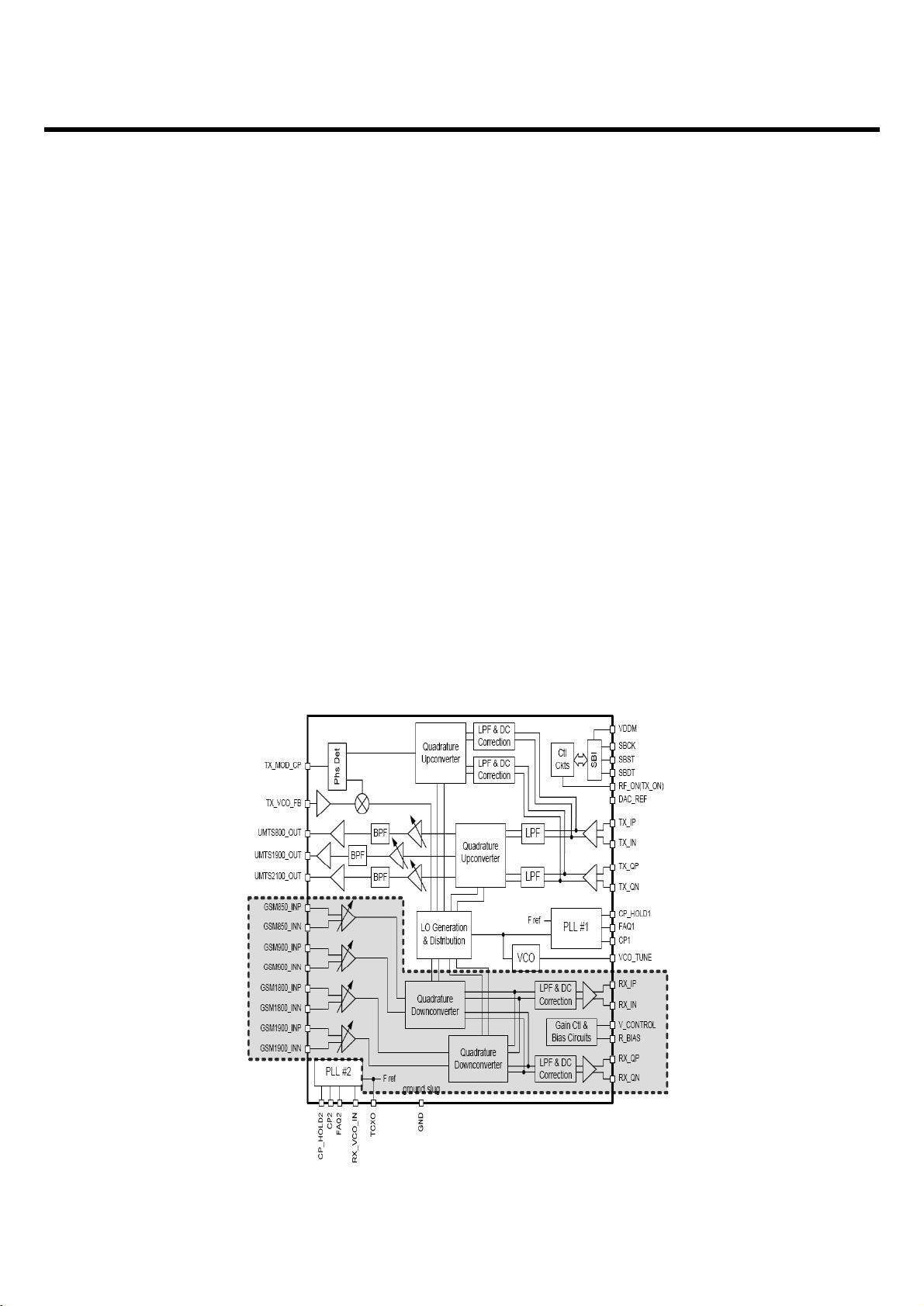
3.1 General Description
The MU500/MU550 supports UMTS-850, UMTS-1900, GSM-850, GSM-900, DCS-1800, and PCS1900 based GSM/GPRS/EDGE/UMTS/HSDPA. All receivers and the UMTS transmitter use the
radioOne1Zero-IF architecture to eliminate intermediate frequencies, directly converting signals
between RF and baseband. The quad-band GSM transmitters use a baseband-to-IF upconversion
followed by an offset phaselocked loop that translates the GMSK-modulated or 8-PSK-modulated
signal to RF.
1
QUALCOMM’s branded chipset that implements a Zero-IF radio architecture.
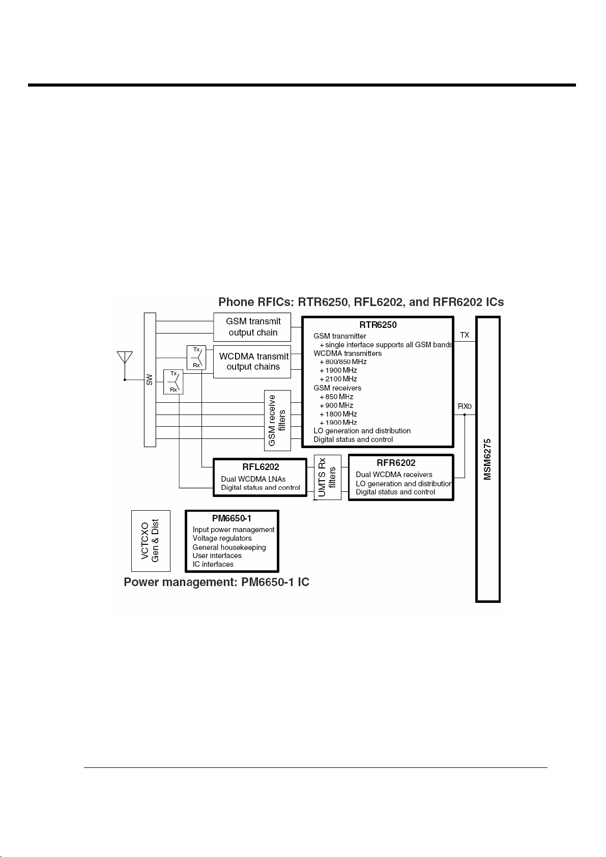
3. TECHNICAL BRIEF
Fig 3.1 Block diagram of RF part

- 18 -
Copyright © 2008 LG Electronics. Inc. All right reserved.
Only for training and service purposes
LGE Internal Use Only
A generic, high-level functional block diagram of MU500/MU550 is shown in Figure 3-1. One antenna collects
base station forward link signals and radiates handset reverse link signals. The antenna connects with receive
and transmit paths through a switch module (plus two duplexers for UMTS high-band and low-band operations).
The UMTS receive signal is amplified by the RFL6202 LNA then passes through a bandpass filter before being
applied to the RFR6202 Receiver IC. On-chip circuits downconvert the received signal directly from RF to
baseband using radioOne Zero-IF techniques. Generation of the UMTS downconverter LO is distributed between
the RTR6250 (phase-locked loop), the RFR6202 (buffer amplifiers and LO distribution circuits) and external UHF
VCO and loop filter circuits. The RFR6202 IC outputs analog baseband signals for further processing by the MSM
device. This baseband interface is shared with the RTR6250 GSM850/GSM900/DCS/PCS receiver outputs.
GSM850, GSM-900, DCS and PCS receive signals pass through their bandpass filters then are applied to the
RTR6250 IC. Similar to the UMTS path, RTR6250 circuits downconvert the received signals directly from RF to
baseband. The GSM850/GSM900/DCS/PCS downconverter LO is generated mostly within the RTR6250 (PLL
and distribution functions); the UMTS Rx CH VCO and loop filter are off-chip. The RTR analog baseband outputs
are routed to the MSM6275 IC for further processing (an interface shared with the RFR).
The UMTS transmit path begins with analog baseband signals from the MSM device that drive the RTR6250 IC.
Integrated PLL and VCO circuits generate the Tx LO used in the quadrature upconverter that translates baseband
signals directly to RF. The RTR6250 output driver stages deliver fairly high-level signals that are filtered and
applied to the power amplifiers (PA). The PA output is routed to the antenna through a duplexer and switch
module.
The shared GSM-850, GSM900, DCS-1800, and PCS-1900 transmit path begins with the same baseband
interface from the MSM6275 IC that is used for the UMTS band. A single GSM850/GSM900/DCS/PCS quadrature
upconverter translates the GMSK or 8-PSK-modulated signal to a convenient intermediate frequency (IF) that
forms one input to an offset phase-locked loop (OPLL). OPLL functions are split between the RTR6250 IC and offchip loop filter and dual Tx VCO circuits, and translate the GMSK or 8-PSK-modulated signal to the desired GSM850, GSM-900, DCS-1800 or PCS-1900 channel frequency. This signal is applied to a dual power amplifier (only
one is active at a time). The enabled path continues with the PA, an automated power control (APC) circuit that
samples the transmit power and adjusts its level, the switch module (which includes a band-appropriate lowpass
filter), and the antenna.
MU500/MU550 power supply voltages are managed and regulated by the PM6650 Power Management IC. This
versatile device integrates all wireless handset power management, general housekeeping, and user interface
support functions into a single mixed signal IC. It monitors and controls the external power source and coordinates
battery recharging while maintaining the handset supply voltages using low dropout, programmable regulators.
The device’s general housekeeping functions include an ADC and analog multiplexer circuit for monitoring on-chip
voltage sources, charging status, and current flow, as well as user-defined off-chip variables such as temperature,
RF output power, and battery ID. Various oscillator, clock, and counter circuits support IC and higher-level
handset functions. Key parameters such as under-voltage lockout and crystal oscillator signal presence are
monitored to protect against detrimental conditions.
3. TECHNICAL BRIEF
- 19 -
Copyright © 2008 LG Electronics. Inc. All right reserved.
Only for training and service purposes
LGE Internal Use Only
3. TECHNICAL BRIEF
3.2 GSM Mode
3.2.1 GSM Receiver
The Dual-mode MU500/MU550’s receiver functions are split between the three RFICs as follows:
• UMTS-850,1900 operation uses the RFL6202 LNA and RFR6202 Receiver ICs to implement the
receive signal path, accepting an RF input and delivering analog baseband outputs (I and Q).
• GSM-850, GSM-900, DCS-1800, and PCS-1900 modes both use the RTR6250 IC only. Each mode
has independent front-end circuits and down-converters, but they share common baseband circuits
(with only one mode active at a time). All receiver control functions are beginning with SBI2-controlled
parameters.
RF Front end consists of antenna, antenna switch module(CXG1198AEQ), and three RX saw
filters(GSM850, GSM900, DCS and PCS). The antenna switch module allows multiple operating
bands and modes to share the same antenna. In MU500/MU550, a common antenna connects to one
of eight paths: 1) UMTS-850 Rx/Tx, 2) UMTS-1900 Rx/Tx, 3) GSM-850 Rx, 4) GSM-900 Rx, 5) GSM850 GSM-900 Tx, (Low Band Tx’s share the same path) 6) DCS-1800 Rx, and 7) DCS-1800,PCS1900 Tx(High Band Tx’s share the same path), 8) PCS-1900 Rx. UMTS operation requires
simultaneous reception and transmission, so the UMTS Rx/Tx connection is routed to a duplexer that
separates receive and transmit signals. GSM850/GSM900, DCS, and PCS operation is time division
duplexed, so only the receiver or transmitter is active at any time and a frequency duplexer is not
required.
2
The RFIC operating modes and circuit parameters are MSM-controlled through the proprietary 3-line Serial Bus Interface (SBI). The Application
Programming Interface (API) is used to implement SBI commands. The API is documented in AMSS Software - please see applicable AMSS
Software documentation for details.
IN_A IN_B IN_C
GSM850/GSM900 TX HIGH HIGH LOW
DCS/PCS TX HIGH LOW LOW
GSM 850 RX LOW HIGH LOW
UMTS 850 HIGH LOW HIGH
DCS RX LOW HIGH HIGH
PCS RX LOW LOW HIGH
UMTS 1900 HIGH HIGH HIGH
GSM 900 LOW LOW LOW
Table 3.2.1 Antenna Switch Module Control logic
- 20 -
Copyright © 2008 LG Electronics. Inc. All right reserved.
Only for training and service purposes
LGE Internal Use Only
The GSM850, GSM900, DCS, and PCS receiver inputs of RTR6250 are connected directly to the transceiver
front-end circuits(filters and antenna switch module). GSM850, GSM900, DCS, and PCS receiver inputs are
similar to the RFR6202 UMTS Rx input in that they also use differential configurations to improve commonmode
rejection and second-order non-linearity performance. The balance between the complementary signals is critical
and must be maintained from the RF filter outputs all the way into the IC pins
Since GSM850, GSM900, DCS, and PCS signals are time-division duplex (the handset can only receive or
transmit at one time), switches are used to separate Rx and Tx signals in place of frequency duplexers - this is
accomplished in the switch module.
The GSM850, GSM900, DCS, and PCS receive signals are routed to the RTR6250 through band selection filters
and matching networks that transform single-ended 50-Ω sources to differential impedances optimized for gain
and noise figure. Similar to the RFR, the RTR input uses a differential configuration to improve second-order intermodulation and common mode rejection performance. The RTR6250 input stages include MSM-controlled gain
adjustments that maximize receiver dynamic range.
The amplifier outputs drive the RF ports of the quadrature RF-to-baseband downconverters. The downconverted
baseband outputs are multiplexed and routed to lowpass filters (one I and one Q) having passband and stopband
characteristics suitable for GMSK or 8-PSK processing. These filter circuits include DC offset corrections. The
filter outputs are buffered and passed on to the MSM6275 IC for further processing (an interface shared with the
RFR6202 UMTS receiver outputs).
3. TECHNICAL BRIEF
Figure 3.2.1 RTR6250 RX feature
- 21 -
Copyright © 2008 LG Electronics. Inc. All right reserved.
Only for training and service purposes
LGE Internal Use Only
3. TECHNICAL BRIEF
3.2.2 GSM Transmitter
The shared GSM Low-band (GSM850/GSM900) and High-band (DCS1800, PCS1900) transmit path begins
with the baseband inputs from the MSM6275 IC. These differential analog input signals are buffered,
lowpass filtered, corrected for DC offsets then applied to the GSM quadrature upconverter. The upconverter
LO signals are generated from the transceiver VCO signal by the LO distribution and generation circuits
within RTR6250. This upconverter translates the GMSK or 8-PSK-modulated signal to a convenient
intermediate frequency (IF) that forms one input to a frequency/phase detector circuit. This IF signal is the
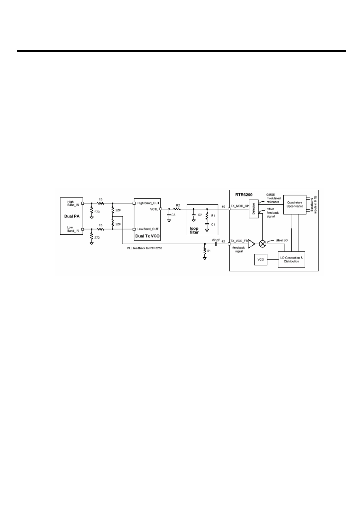
reference input to an offset phase-locked loop (OPLL) circuit as shown in Figure 3.2.2-1.
The feedback path of this OPLL circuit includes a downconversion from the RF output frequency range
to the IF range. The two inputs to this downconversion mixer are formed as follows:
1. The dual Tx VCO output (operating in the desired RF output frequency range) is buffered within the
RTR6250 IC then applied to the mixer RF port.
2. The LO Generation and Distribution circuits that deliver the transmit path.s LO for the baseband-to-IF
upconversion also provides the .offset LO. signal that is applied to the feedback path.s mixer LO port.
The mixer IF port output is the offset feedback signal - the variable input to the frequency/phase
detector circuit. The detector compares its variable input to its reference input and generates an error
signal that is lowpass filtered by the loop filter and applied to the dual Tx VCO tuning port to force the
VCO output in the direction that minimizes errors. As mentioned earlier, the VCO output is connected to
the feedback path thereby creating a closed-loop control system that will force frequency and phase
errors between the variable and reference inputs to zero.
Figure 3.2.2-1 Offset phase-locked loop interfaces

- 22 -
Copyright © 2008 LG Electronics. Inc. All right reserved.
Only for training and service purposes
LGE Internal Use Only
The waveform at the dual Tx VCO output is the GMSK or 8-PSK-modulated signal centered at the
desired GSM channel frequency. A phase-locked loop circuit is used to translate the GMSK or 8-PSKmodulated signal from IF to RF primarily for two reasons:
1. Phase-locked loops provide a lowpass filter function from the reference input to the VCO output. This
results in a bandpass function centered at the desired channel frequency that provides steep, wellcontrolled rejection of the out-of-band spectrum.
2. The resulting output bandpass function is virtually unchanged as the transmitter is tuned over
channels spanning the GSM operating band.
The PA is a key component in any transmitter chain and must complement the rest of the transmitter
precisely. For GSM band operation, the closed-loop transmit power control functions add even more
requirements relative to the UMTS PA. In addition to gain control and switching requirements, the usual
RF parameters such as gain, output power level, several output spectrum requirements, and power
supply current are critical. The gain must be sufficient and variable to deliver the desired transmitter
output power given the VCO output level, the subsequent passive devices’ losses, and the control set
point. The maximum and minimum transmitter output power levels depend upon the operating band
class and mobile station class per the applicable standard. Transmitter timing requirements and inband
and out-of-band emissions, all dominated by the PA, are also specified by the applicable standard.
The active dual Tx VCO output is applied to the dual power amplifier to continue the transmit path, and
feedback to the RTR6250 IC to complete the frequency control loop. The PA operating band
(GSM850/GSM900 or DCS/PCS) is selected by the MSM device GPIO control (GSM_PA_BAND).
3.3 UMTS Mode
3.3.1 Receiver
The UMTS duplexer receiver output is routed to LNA circuits within the RFL6202 device. These LNA
functions are removed from the RFR6202 IC to improve mixer LO to RF isolation - a critical parameter
in the Zero-IF architecture. Isolation is further improved using high reverse isolation circuits in the LNA
designs. The LNA gain is controlled by the MSM device to minimize DC power consumption while
achieving the desired RF performance.
3. TECHNICAL BRIEF
- 23 -
Copyright © 2008 LG Electronics. Inc. All right reserved.
Only for training and service purposes
LGE Internal Use Only
3. TECHNICAL BRIEF
The UMTS LNA output is routed to the RFR6202 through a band selection filter that transforms a
single-ended 50
Ω
source to a differential impedance that is matched to the RFR6202 IC. The RFR input
uses a differential configuration to improve second-order inter-modulation and common mode rejection
performance. The RFR6202 input stages include MSM-controlled gain adjustments that further extend
receiver dynamic range.
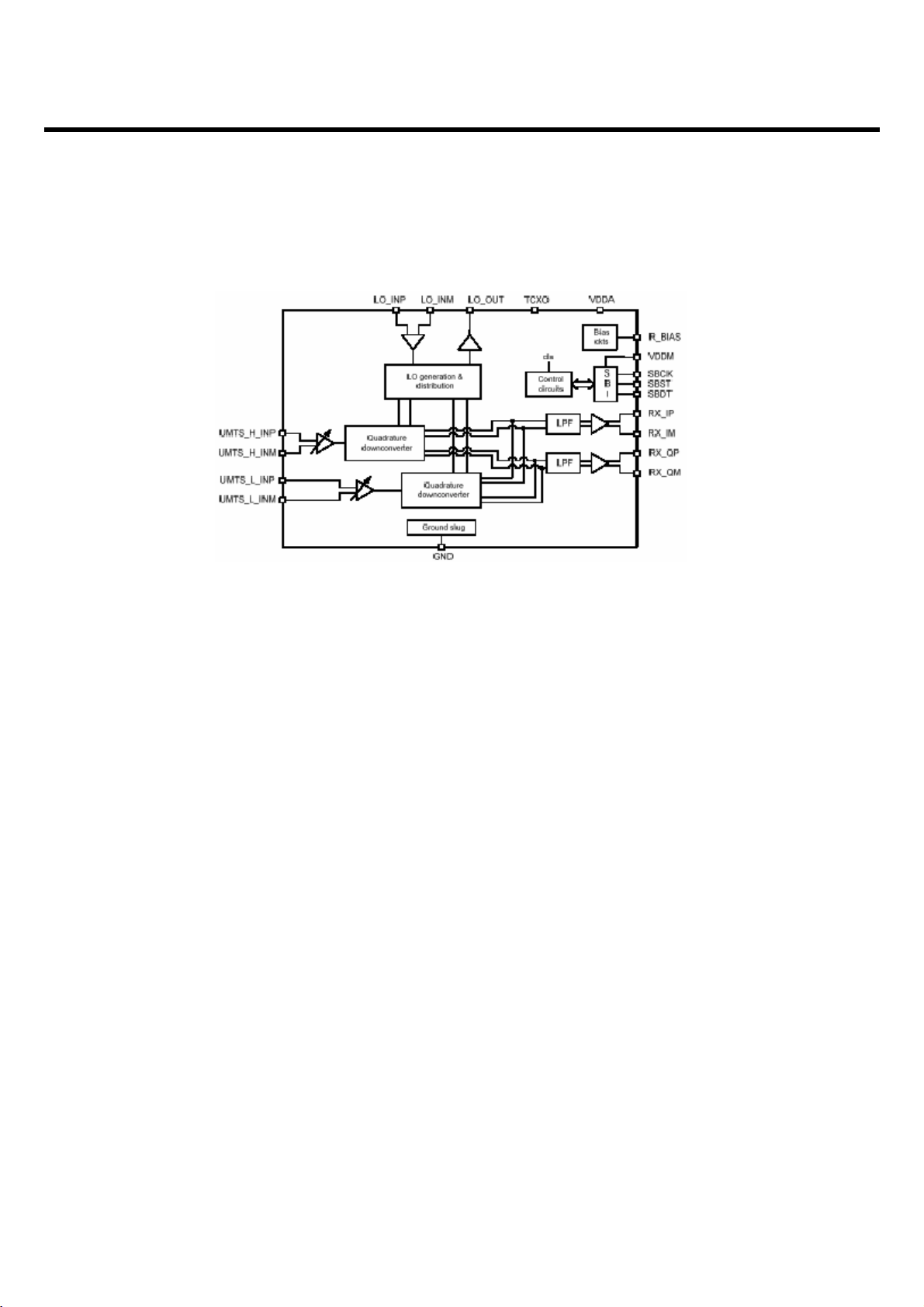
The RFR6202 IC (Figure 3.3.1-1) provides the UMTS Zero-IF receiver signal path, from RF to analog
baseband. The input gain stage implements MSM controlled gain adjustments to extend receiver
dynamic range. The amplifier output drives the RF port of the quadrature RF-to-baseband
downconverter then the downconverted baseband outputs are routed to lowpass filters (one I and one
Q) whose passband and stopband characteristics are suitable for DS-WCDMA signals. The filter
outputs are buffered and routed to the MSM device for further processing. This baseband interface is
shared with the RTR6250 GSM850/GSM900/DCS/PCS receiver outputs.
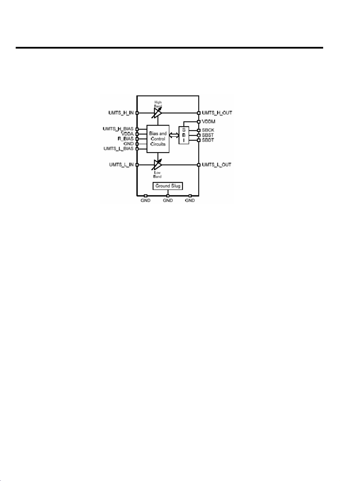
Figure 3.3.1-1 RFL6202 IC functional block diagram
- 24 -
Copyright © 2008 LG Electronics. Inc. All right reserved.
Only for training and service purposes
LGE Internal Use Only
The RFR6202 IC includes LO generation and distribution circuitry to reduce offchip component
requirements. The UMTS Rx LO source is created using an external UMTS Rx CH VCO that is closedloop controlled by the RTR6250 PLL2 via a discrete loop filter. The external UMTS_RX_VCO signal is
processed by the LO generation and distribution circuits to create the quadrature downconverter LO
signal. The LO signal applied at the mixer ports are at a frequency different than the VCO frequency.
This assures that the VCO frequency is different than the RF frequency, an important consideration for
Zero-IF processing. QUALCOMM.s Mobile Station Modem (MSM6275) device provides status and
control signaling, employing power reduction features (such as selective circuit power-down, gain
control, and bias control) to extend handset standby time.
3. TECHNICAL BRIEF
Figure 3.3.1-2 RFR6202 IC functional block diagram

- 25 -
Copyright © 2008 LG Electronics. Inc. All right reserved.
Only for training and service purposes
LGE Internal Use Only
3. TECHNICAL BRIEF
3.3.2 Transmitter
The UMTS transmit path begins with analog baseband signals from the MSM device that drive the
RTR6250 IC. The RTR6250 IC provides all the UMTS transmitter active signal-path circuits except the
power amplifiers. Analog (I and Q) differential signals from the MSM device are buffered, filtered, and
applied to Baseband-to-RF quadrature upconverters. Gain control is implemented on-chip.
The RF outputs include an integrated matching inductor, reducing the off-chip matching network to a
single series capacitor.
The RTR6200 UMTS output is routed to its power amplifier through a bandpass filter, and delivers
fairly high-level signals that are filtered and applied to the PA. The PA device used in MU500/MU550 is
°∞Load Insensitive PA°±- no need to use isolator - and routed to the duplexer Tx port directly.
Transmit power is delivered from the duplexer to the antenna through the switch module.
The RTR6250 IC integrates LO generation and distribution circuits on-chip, substantially reducing offchip requirements. Various modes and programmable features result in a highly flexible transceiver LO
output that supports not only UMTS transmissions, but all GSM850/900 and DCS1800/PCS1900 Rx
and Tx modes as well.
The UMTS Tx LO (PLL1) is generated almost entirely on-chip, requiring only the loop filter off-chip
(two capacitors and two resistors); all UMTS Tx VCO and PLL circuits are on-chip. An internal
RTR6250 switch routes the internal VCO signal to the LO generation and distribution circuits to create
the necessary UMTS Tx LO signals.
- 26 -
Copyright © 2008 LG Electronics. Inc. All right reserved.
Only for training and service purposes
LGE Internal Use Only
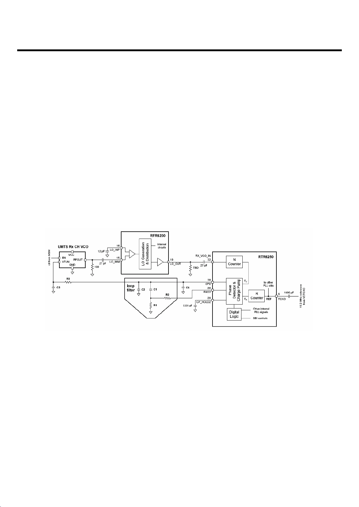
3.4 LO Phase-locked Loop
Most LO functions are fully integrated on-chip, do not require user adjustment, and need not be
considered by handset designers. QUALCOMM has established and implemented frequency plans
and LO generation schemes that support the radioOne 6250-IIseries chipset while requiring minimal
off-chip design effort. Only one area requires handset designer attention: the loop filters of each
phase-locked loop (PLL).
3.4.1 UMTS Rx PLL (PLL2)
UMTS Rx LO functional blocks are distributed between the RFR6202 IC, RTR6250 IC, and external
UMTS_RX_CH_VCO and loop filter components (Figure 3.4.1-1). The external UMTS_RX_CH_VCO
must be enabled for UMTS Rx operation and disabled otherwise; a dedicated MSM6275 IC signal
(UHF_VCO_EN ) enables the VCO.
The RFR6202 IC accommodates single-ended or differential LO inputs; if singleended, either pin can
be active. AC-couple the inactive pin to ground using an appropriately valued capacitor (12 pF is used
in MU500/MU550). The 27 pF capacitor should be used to AC-couple the active pin to the VCO signal.
Using only the selected VCO signal, the RFR6202 IC LO generation and distribution circuits create the
necessary LO signals for the active quadrature downconverter.
A sample of the downconverter LO is buffered and routed from RFR6202 IC pin 19 to RTR6250 IC pin
32 (RX_VCO_IN). This signal requires a terminating resistor near the RTR6250 IC input pin and an AC
coupling capacitor that assures the internal RTR6250 IC biasing is not disrupted in the example. Good
microstrip or stripline controlled-impedance techniques must be used
3. TECHNICAL BRIEF
Figure 3.4.1-1 UMTS Rx PLL functional block diagram
- 27 -
Copyright © 2008 LG Electronics. Inc. All right reserved.
Only for training and service purposes
LGE Internal Use Only
3. TECHNICAL BRIEF
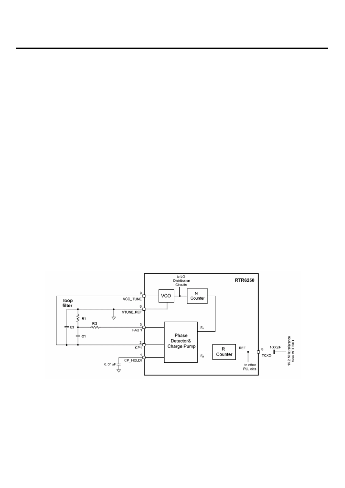
Most UMTS Rx PLL circuits are included within the RTR6250 IC: reference divider, phase detector,
charge pump, feedback divider, and digital logic that generate LOCK status. The buffered 19.2 MHz
TCXO signal provides the synthesizer input (REF), the frequency reference to which the PLL is phase
and frequency locked. The reference is divided by the R-Counter to create a fixed frequency input to
the phase detector, FR. The other phase detector input (FV) varies as the loop acquires lock, and is
generated by dividing the RX_VCO_IN frequency using the feedback path.s N-Counter. The closed
loop will force FV to equal FR when locked. If the loop is not locked the error between FV and FR will
create an error signal at the output of the charge pump. This error signal is filtered by the loop filter
and applied to the VCO, tuning the output frequency such that the error is decreased. Ultimately the
loop forces the error to approach zero and the PLL is phase and frequency locked.
Many key PLL performance characteristics are largely determined by the loop filter design - stability,
transitory response, settling time, and phase noise.
3.4.2 Transceiver PLL (PLL1)
All LO functional blocks for the other handset modes(UMTS Tx, GSM850/GSM900 Tx/Rx, DCS Tx/Rx,
PCS Tx/Rx) are integrated into the RTR6250 IC except the loop filter components (Figure 3.4.2-1).
On-chip circuits include reference divider, phase detector, charge pump, VCO, feedback divider, and
digital logic status. The functional description given in Section 3.4.1 for the UMTS Rx PLL applies to
the Transceiver PLL as well.
The off-chip loop filter allows optimization of key PLL performance characteristics (stability, transitory
response, settling time, and phase noise) for different applications. Guidelines are provided in the next
subsection for proper implementation of this critical circuit.
Figure 3.4.2-1 Transceiver PLL functional block diagram

- 28 -
Copyright © 2008 LG Electronics. Inc. All right reserved.
Only for training and service purposes
LGE Internal Use Only
3.5 Off-chip RF Components
3.5.1 Antenna switch module (U100 : CXG1198AEQ)
The antenna switch module allows multiple operating bands and modes to share the same antenna. In
the MU500/MU550 design, a common antenna connects to one of eight paths: 1) UMTS-850 Rx/Tx, 2)
UMTS-1900 Rx/Tx, 3) GSM-850 Rx, 4) GSM-900 Rx, 5) GSM-850/GSM-900 Tx(Low Band Tx’s share
the same path), 6) DCS-1800 Rx, and 7) DCS-1800,PCS-1900 Tx(High Band Tx’s share the same
path), 8) PCS-1900 Rx. UMTS operation requires simultaneous reception and transmission, so the
UMTS Rx/Tx connection is routed to a duplexer that separates receive and transmit signals. GSM
band of operation is time division duplexed, so only the receiver or transmitter is active at any time and
a frequency duplexer is not required. The module includes lowpass filters for the GSM bands transmit
paths to reduce out-of-band emissions, PA harmonics in particular.
3.5.2 UMTS duplexer (FL106_
UMTS1900 : ACMD7402 , FL107_UMTS850 : B7637 )
A UMTS duplexer splits a single operating band into receive and transmit paths. Important performance
requirements include;
-. Insertion loss . this component is also in the receive and transmit paths ; In the MU500/MU550 typical losses :
UMTS1900_ Tx = 2.1 dB, UMTS1900_ Rx = 2.8 dB and UMTS850_ Tx =1.9 dB, UMTS850_ Rx = 2.7 dB
-. Out-of-band rejection or attenuation . the duplexer provides input selectivity for the receiver, output filtering for
the transmitter, and isolation between the two. Rejection levels for both paths are specified over a number of
frequency ranges. Two Tx-to-Rx isolation levels are critical to receiver performance:
-. Rx-band isolation . the transmitter is specified for out-of-band noise falling into the Rx band. This noise leaks
from the transmit path into the receive path, and must be limited to avoid degrading receiver sensitivity. The
required Rx-band isolation depends on the PA out of-band noise levels and Rx-band losses between the PA
and LNA. Minimum duplexer Rx band isolation value is about 45 dB.
-. Tx-band isolation . the transmit channel power also leaks into the receiver. In this case, the leakage is outside
the receiver passband but at a relatively high level. It combines with Rx band jammers to create crossmodulation products that fall in-band to desensitize the receiver. The required Tx-band isolation depends on the
PA channel power and Tx-band losses between the PA and LNA. Minimum duplexer Tx-band isolation value is
about 55 dB.
-. Passband ripple . the loss of this fairly narrowband device is not flat across its passband. Passband ripple
increases the receive or transmit insertion loss at specific frequencies, creating performance variations across
the band.s channels, and should be controlled.
-. Return loss . minimize mismatch losses with typical return losses of 10 dB or more (VSWR <2:1).
-. Power handling . high power levels in the transmit path must be accommodated without degraded
performance. The specified level depends on the operating band class and mobile station class (per
the applicable standard), as well as circuit losses and antenna EIRP. Several duplexer
characteristics depend upon its source and load impedances. QUALCOMM strongly recommends an
isolator be used between the UMTS PA and duplexer to assure proper performance.
3. TECHNICAL BRIEF
- 29 -
Copyright © 2008 LG Electronics. Inc. All right reserved.
Only for training and service purposes
LGE Internal Use Only
3. TECHNICAL BRIEF
3.5.3 UMTS Power Amplifier (U105 : RF5144)
-. U105 : UMTS 850 Power Amplifier module
The RF5144 is a high-power, high-efficiency linear amplifier module specifically designed for 3V
handheld systems. The device is manufactured on an advanced third generation GaAs HBT process,
and was designed for use as the final RF amplifier in 3V UMTS handheld digital cellular equipment,
spread-spectrum systems, and other applications in the 824MHz to 849MHz band and 1850MHz to
1910MHz band. The RF5144 has a digital control line for low power applications to lower quiescent
current.
3.5.4 Thermistor (R1024 : 68K_2012_10%)
This thermistor senses temperature variations around UMTS PA to adjust PA gain deviation for assure
compliance with the applicable transmit power control standards. Negative temperature compensation
thermistor is used in the MU500/MU550.
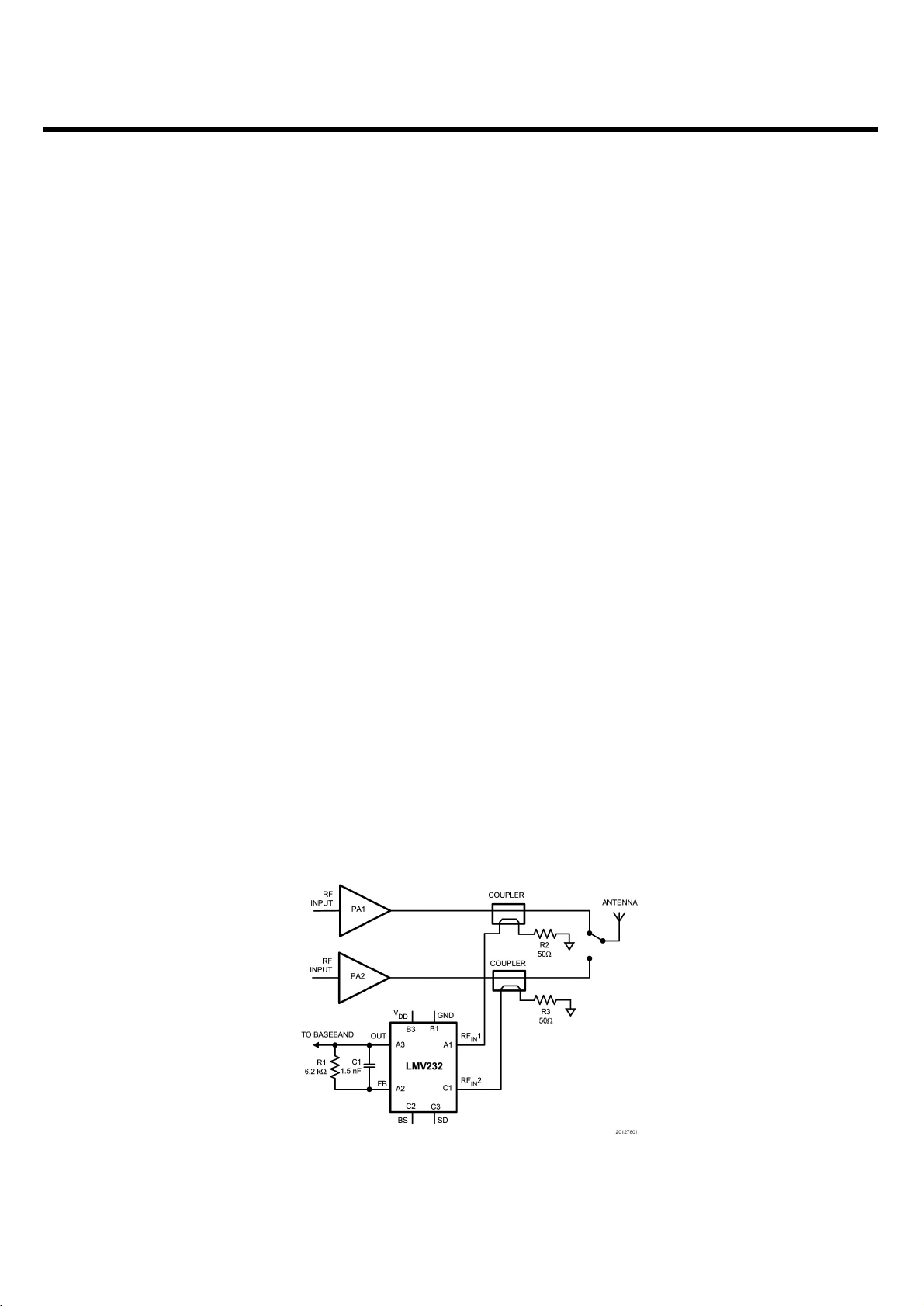
3.5.5 UMTS transmit power detector (U107 : LMV232TLX)
This detector couples PA output power level to calibrate the transmitter characteristic over the channel
variation and temperature. Its detector coupling range and converted voltage is based on diode
sensitivity and transmitter power level.
The MU500/MU550 uses National Semiconductor LMV232TLX power detector IC. In Figure 3.5.5-1,
RF input power range of the device has been optimized for use with a 20dB directional coupler,
without the need for additional external componets. The device has two digital interfaces. A Shutdown
function is available to set the device in a low-power shutdown mode. In case SD=High, the device is
in shutdown, if SD=LOW the device is active.The Band-Select function controls the selection of the
active RF input channel. In case BS=HIGH, Rfin1 is active. In case BS=LOW, Rfin2 is active.
Figure 3.5.5-1 Block diagram of LMV232TLX with Coupler
- 30 -
Copyright © 2008 LG Electronics. Inc. All right reserved.
Only for training and service purposes
LGE Internal Use Only
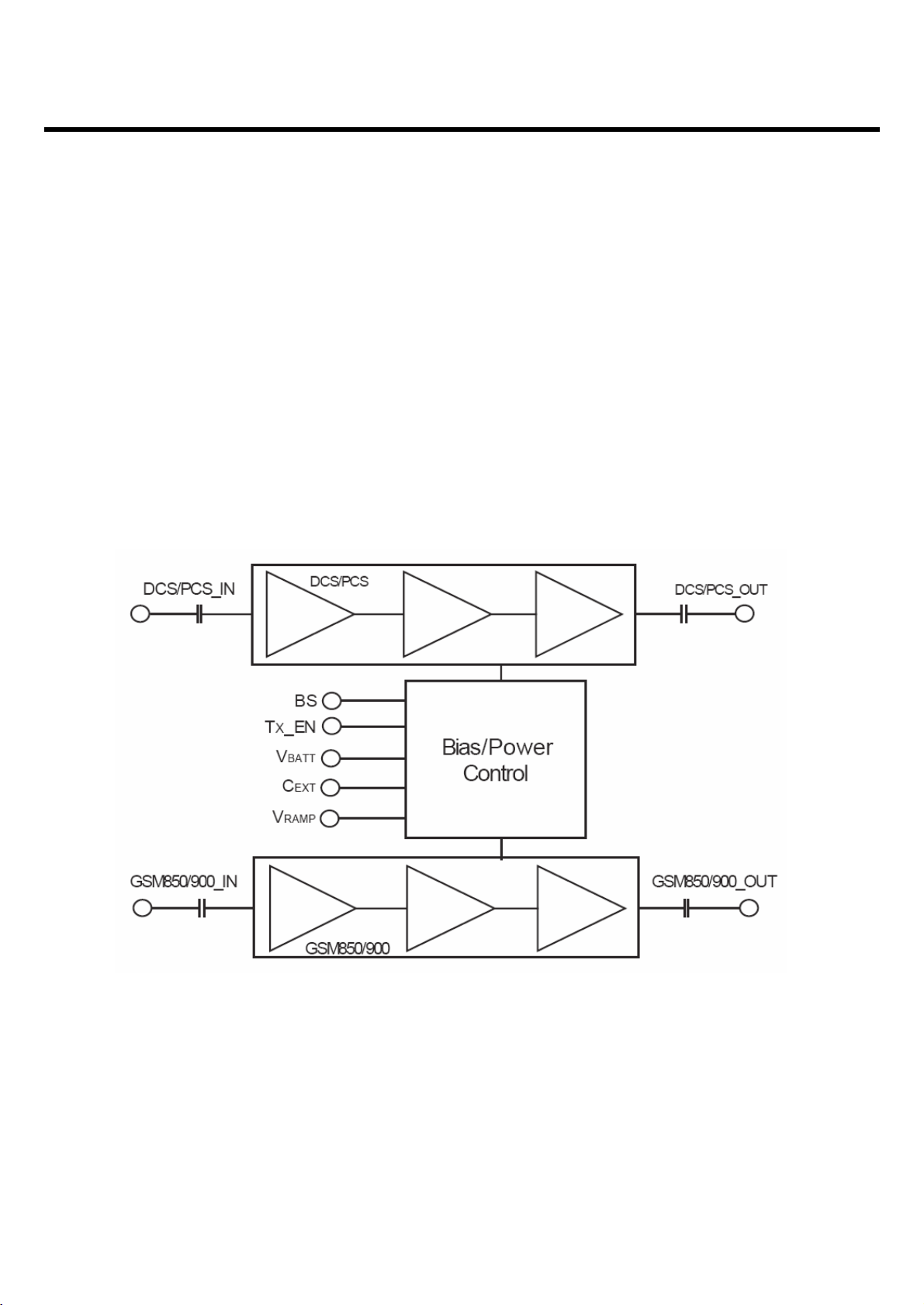
3.5.6 GSM/GPRS/EDGE Power amplifier (U102 : AND0041)
This power amplifier module is designed in a low profile (1.3 mm) and supports dual, tri and quad band
applications for GMSK and 8-PSK modulation schemes using a polar architecture. There aretwo
amplifier chains, one to support GSM850/900 bands, the other for DCS/PCS bands.
The module includes an internal reference voltage and integrated power control scheme for use in
both GMSK and 8-PSK operation. This facilitates fast and easy production calibration and reduces the
number of external components required to complete a power control function. The amplifier's power
control range is typically 55 dB, with the output power set by applying an analog voltage to VRAMP.
All of the RF ports for this device are internally matched to 50Ω . Internal DC blocks are provided at
the RF inputs.
3. TECHNICAL BRIEF
Figure 3.5.6-1 GSM PA functional block diagram

- 31 -
Copyright © 2008 LG Electronics. Inc. All right reserved.
Only for training and service purposes
LGE Internal Use Only
3. TECHNICAL BRIEF
3.5.7 GSM transmit VCO (X101 : MQW5V0C869M)
The dual Tx VCO is a key component within the GSM OPLL. This VCO performance directly impacts
PLL and transmitter performance. VCO specifications refer to muRata MQW5V0C869M datasheet.
The dual Tx VCO outputs, one for Low-band GSM and one for high band, drive a resistive network that
splits the active signal into two signals: 1) the input to the active PA . this is the low loss path, and 2)
the OPLL feedback signal . this is the high loss path.
The losses from the VCO outputs to the PA inputs must be factored into the output chain.s power
budget. Each path includes a π-pad that introduces approximately a 3-dB loss. The low band GSM πpad is formed by R1014 plus R1018, R1021, and R1022; the high band GSM π-pad is formed by
R1016 plus R1019, R1020, and R1022. One leg of each π-pad is used to couple the VCO output to
form the feedback path as described below.
For a given VCO output drive level, the loss to the RTR6250 input must assure the specified input
level is achieved (-18 to -12 dBm). Large resistors included in the π-pads are used to lightly couple off
the VCO outputs to create the feedback signal.
Since the RTR6250 TX_VCO_FB pin presents fairly high impedance, an external terminating resistor
is required (R1022, 51 Ω). A series capacitor (82 pF) AC couples the feedback signal into the
RTR6250 IC.
3.5.8 UMTS Rx RF filter (FL109, FL110)
FL109 - B7837 869 ~ 894MHz GSM850 Rx RF filter
FL110 - B7847 1805 ~1880MHz USPCS1800 Rx RF filter
An RF filter is located between the UMTS LNA and mixer. Insertion loss is important, but not as critical
as losses before the LNA. The most important parameters of this component include:
• Out-of-band rejection or attenuation levels, usually specified to meet these conditions:
- Far out-of-band signals - ranging from DC up to the first band of particular concern and from the
last band of particular concern to beyond three times the highest passband frequency.
- Tx-band leakage - the transmitter channel power, although attenuated by the duplexer, still
presents a cross-modulation threat in combination with Rx-band jammers. The RF filter must
provide rejection of this Tx-band leakage.
- Other frequencies of particular concern . bands known to include other wireless transmitters that
may deliver significant power levels to the receiver input.
• Phase and amplitude balance - the ZIF architecture requires well-balanced differential inputs to the
RFR6202 IC. This is accomplished by the RF filter which takes a single-ended output from the
RFL6202 IC and provides differential outputs having nominal 180°∆ phase separation. Phase and/or
amplitude imbalance causes degraded common-mode rejection and second-order nonlinearity, so
their requirements are specified jointly.
- ±3 degrees and ± 1 dB
- -12 to + 3 degrees and ± 0.7 dB
Of course, passband ripple and return loss are still important in all cases for the same reasons
explained in the antenna switch module and duplexer sections.
 Loading...