

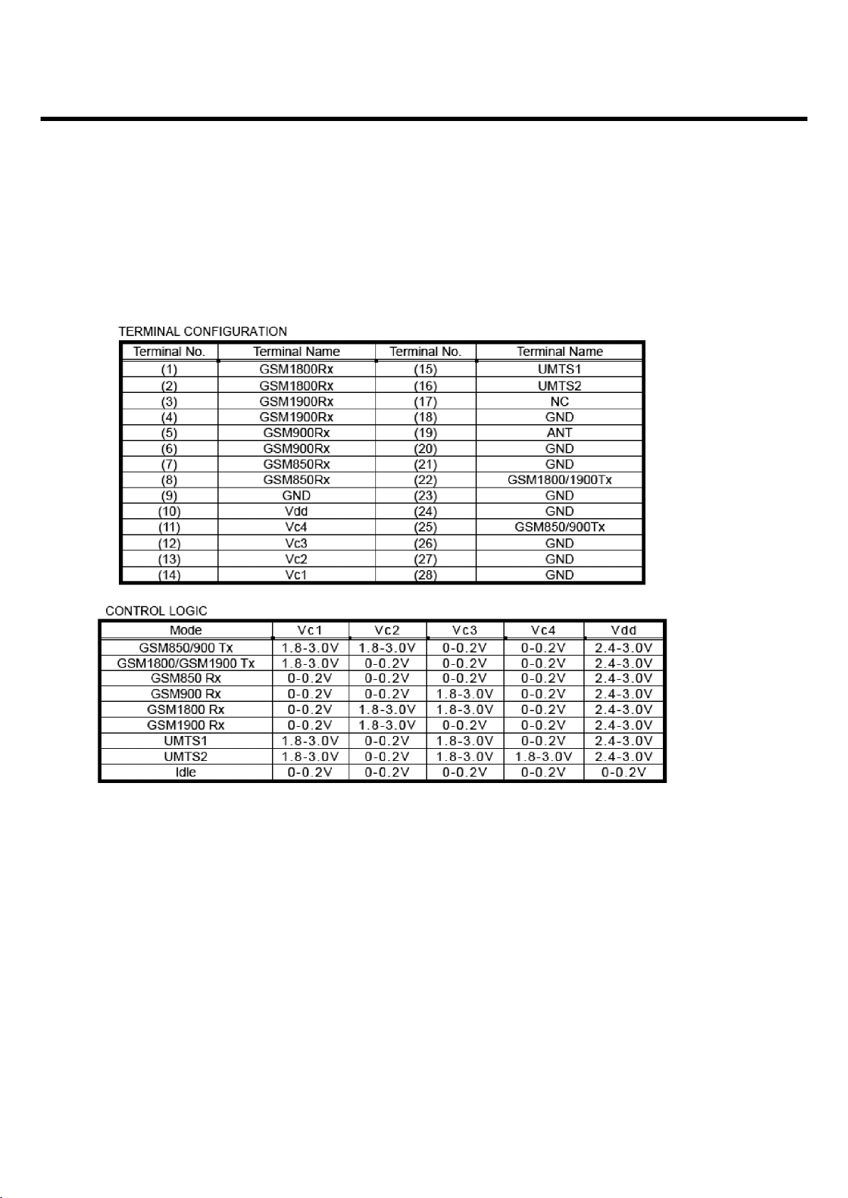
LG MU515 Service Manual
Date: January, 2008 / Issue 1.0
Service Manual
MU515
Service Manual
Model : MU515
Internal Use Only

- 3 -
1. INTRODUCTION .............................. 5
1.1 Purpose................................................... 5
1.2 Regulatory Information............................ 5
2. PERFORMANCE...............................7
2.1 System Specification................................7
2.2 Using Condition (Accessory)....................7
2.3 Radio Performance..................................8
2.4 Current Consumption.............................11
2.5 Operation Time ......................................11
2.6 RSSI Bar................................................11
2.7 Battery Bar.............................................12
2.8 BACKUP BATTERY...............................12
2.9 Sound Level...........................................12
3. TECHNICAL BRIEF ........................13
3.1 General Description ...............................13
3.2 GSM Mode.............................................15
3.3 UMTS Mode...........................................19
3.4 LO Phase-locked Loop ..........................22
3.5 Off-chip RF Components .......................24
3.6 Digital Baseband(DBB/MSM6260).........32
3.7 Block Diagram(MSM6260).....................34
3.8 Subsystem(MSM6260) ..........................35
3.9 Power Block...........................................43
3.10 External memory interface...................48
3.11 H/W Sub System..................................49
3.12 Main Features......................................65
4. TROUBLE SHOOTING ...................69
4.1 RF Component.......................................69
4.2 Checking VCXO Block...........................72
4.3 Checking Ant. SW Module Block ...........74
4.4 Checking UMTS Block...........................76
4.5 Checking GSM Block.............................83
4.6 Power ON Troubleshooting....................92
4.7 Charger Troubleshooting .......................95
4.8 USB Troubleshooting.............................98
4.9 SIM Detect Troubleshooting ................100
4.10 Camera Troubleshooting ...................102
4.11 Keypad Backlight Troubleshooting ....104
4.12 Folder ON/OFF Troubleshooting .......105
4.13 Main LCD Troubleshooting ................106
4.14 Receiver Path ....................................107
4.15 Headset path......................................109
4.16 Speaker phone path...........................111
4.17 Main microphone ...............................113
4.18 Headset microphone..........................115
4.19 Vibrator ..............................................117
5. DOWNLOAD..................................118
5.1 Introduction ..........................................118
5.2 Downloading Procedure.......................118
5.3 Troubleshooting Download Errors .......133
5.4 Caution.................................................141
6. BLOCK DIAGRAM ........................142
6.1 GSM & UMTS RF Block.......................142
6.2 Interface Diagram ................................143
7. Circuit Diagram ............................145
8. BGM Pin Map................................153
9. PCB LAYOUT................................167
10. Calibration & RF Auto Test
Program (Hot Kimchi)................159
10.1 Configuration of HOT KIMCHI ...........159
10.2 How to use HOT KIMCHI...................160
11. EXPLODED VIEW &
REPLACEMENT PART LIST ..... 163
11.1 EXPLODED VIEW ............................ 163
11.2 Replacement Parts
<Mechanic component>.................... 165
<Main component> ........................... 169
11.3 Accessory ......................................... 186
Table Of Contents
LGE Internal Use Only
Copyright © 2007 LG Electronics. Inc. All right reserved.
Only for training and service purposes

- 4 -
LGE Internal Use Only
Copyright © 2007 LG Electronics. Inc. All right reserved.
Only for training and service purposes

LGE Internal Use Only
Copyright © 2007 LG Electronics. Inc. All right reserved.
Only for training and service purposes
- 5 -
1.1 Purpose
This manual provides the information necessary to repair, calibration, description and download the
features of this model.
1.2 Regulatory Information
A. Security
Toll fraud, the unauthorized use of telecommunications system by an unauthorized part (for example,
persons other than your company’s employees, agents, subcontractors, or person working on your
company’s behalf) can result in substantial additional charges for your telecommunications services.
System users are responsible for the security of own system. There are may be risks of toll fraud
associated with your telecommunications system. System users are responsible for programming and
configuring the equipment to prevent unauthorized use. The manufacturer does not warrant that this
product is immune from the above case but will prevent unauthorized use of commoncarrier
telecommunication service of facilities accessed through or connected to it. The manufacturer will not
be responsible for any charges that resultfrom such unauthorized use.
B. Incidence of Harm
If a telephone company determines that the equipment provided to customer is faulty and possibly
causing harm or interruption in service to the telephone network, it should disconnect telephone
service until repair can be done. A telephone company may temporarily disconnect service as long as
repair is not done.
C. Changes in Service
A local telephone company may make changes in its communications facilities or procedure. If these
changes could reasonably be expected to affect the use of the phones or compatibility with the net
work, the telephone company is required to give advanced written notice to the user, allowing the user
to take appropriate steps to maintain telephone service.
D. Maintenance Limitations
Maintenance limitations on the phones must be performed only by the manufacturer or its authorized
agent. The user may not make any changes and/or repairs expect as specifically noted in this manual.
Therefore, note that unauthorized alternations or repair may affect the regulatory status of the system
and may void any remaining warranty.
1. INTRODUCTION
1. INTRODUCTION
LGE Internal Use Only
Copyright © 2007 LG Electronics. Inc. All right reserved.
Only for training and service purposes
E. Notice of Radiated Emissions
This model complies with rules regarding radiation and radio frequency emission as defined by local
regulatory agencies. In accordance with these agencies, you may be required to provide information
such as the following to the end user.
F. Pictures
The pictures in this manual are for illustrative purposes only; your actual hardware may look slightly
different.
G. Interference and Attenuation
A phone may interfere with sensitive laboratory equipment, medical equipment, etc. Interference from
unsuppressed engines or electric motors may cause problems.
H. Electrostatic Sensitive Devices
ATTENTION
Boards, which contain Electrostatic Sensitive Device (ESD), are indicated by the sign.
Following information is ESD handling:
• Service personnel should ground themselves by using a wrist strap when exchange system boards.
• When repairs are made to a system board, they should spread the floor with anti-static mat which is
also grounded.
• Use a suitable, grounded soldering iron.
• Keep sensitive parts in these protective packages until these are used.
• When returning system boards or parts like EEPROM to the factory, use the protective package as
described.
1. INTRODUCTION
- 6 -
LGE Internal Use Only
Copyright © 2007 LG Electronics. Inc. All right reserved.
Only for training and service purposes
2. PERFORMANCE
- 7 -
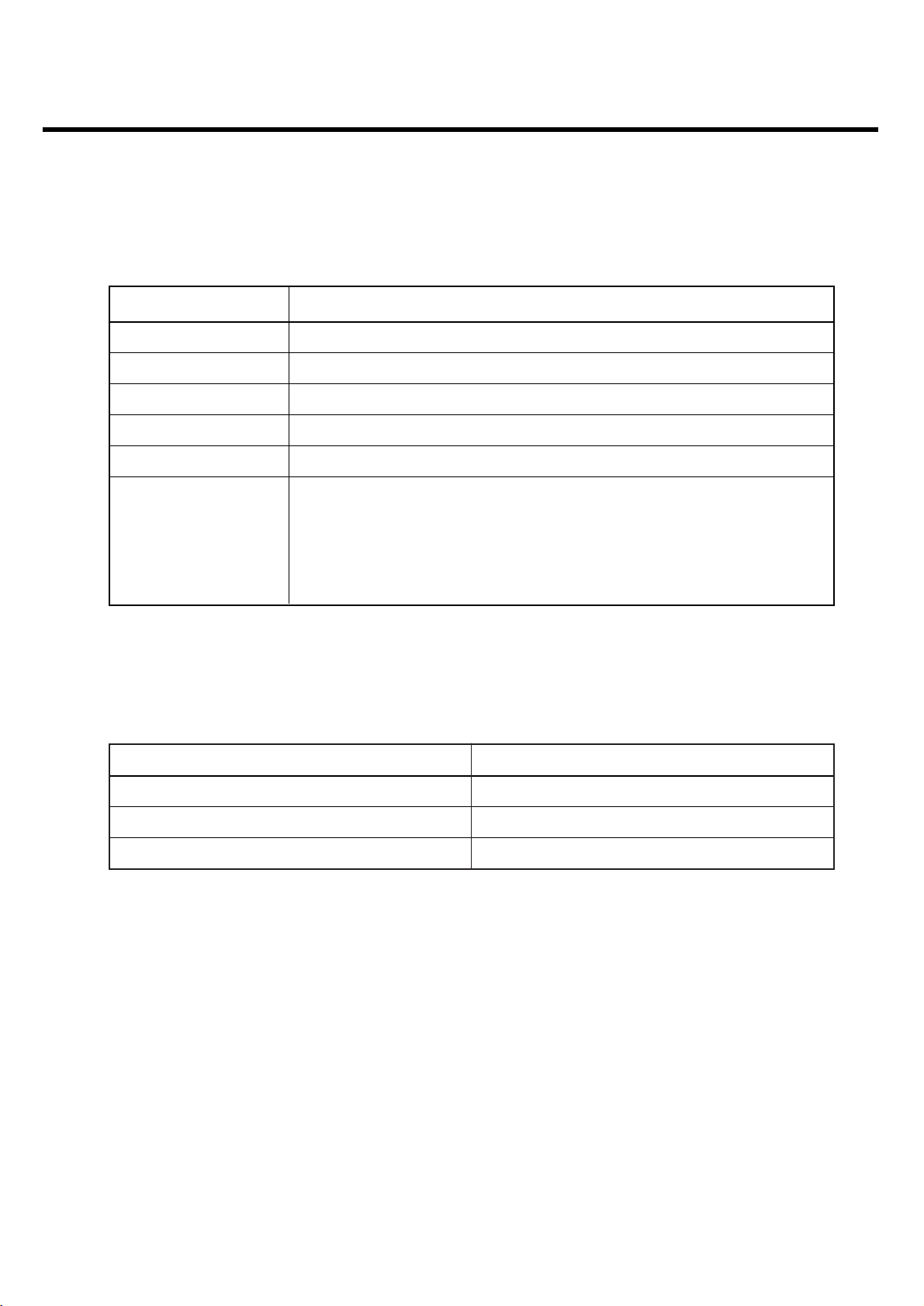
2.1 System Specification
2.2 Using Condition (Accessory)
1) Maximum Using Condition (Using Environment)
2. PERFORMANCE
Item Type / Spec.
1.Type TFT Main_LCD & Mono Sub LCD Folder
2.Size 96 x 49.5 x 18.3 mm
3.Weight 100.5g, (With 1,000mA Battery)
4.Battery Standard :1,000 mAh (Li-ion)
5.LCD Type TFT Main LCD(2’, 176 x 220), Mono Sub LCD(1.3’ 128 X160)
6.Accessory
1)Travel Adaptor 1) Input : AC 100~240V , Output : 5.1V, 700mA
2)Ear-Mic Adaptor 2) ELA
3)Data Cable 3) USB data cable (option)
Item Specification
Available AC Input Power AC : 240 V Max
Available DC Input Power DC : 12 V Max
Storage Temperature - 20 ~ + 70 °C
LGE Internal Use Only
Copyright © 2007 LG Electronics. Inc. All right reserved.
Only for training and service purposes
2) General Using Condition
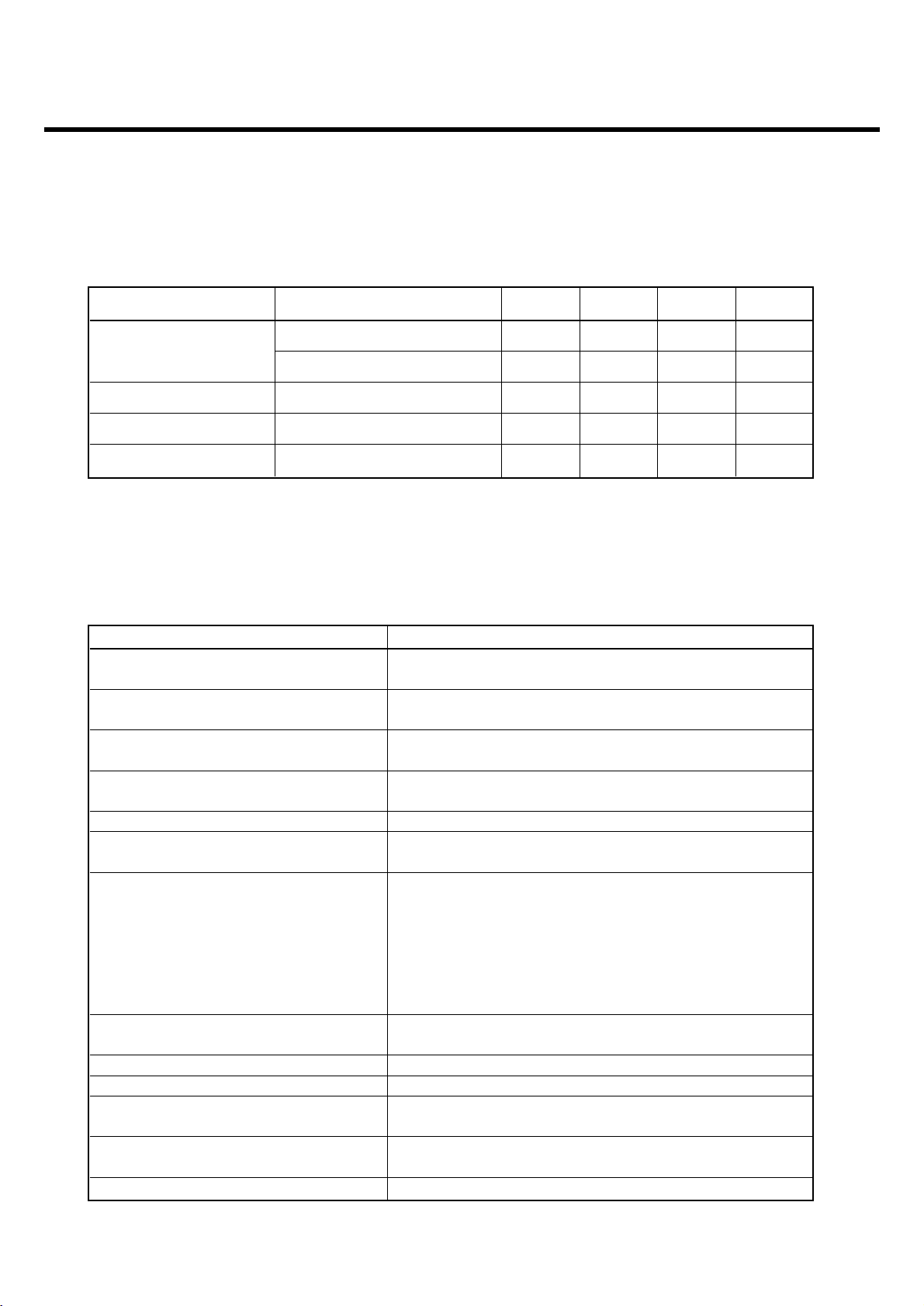
2.3 Radio Performance
1) Transmitter-GSM Mode
2. PERFORMANCE
- 8 -
Item Spec. Min Typ. Max Unit
Output Power
DC Power 12 Vdc
Battery Power 3.2 3.7 4.2 Vdc
Input Power AC Power 100 110 240 Vac
Current Consumption W
Operation Temperature -20 60 °C
Item Specification
Phase Error
Rms : 5°
Peak : 20°
Frequency Error
GSM : 0.1 ppm
DCS/PCS : 0.1 ppm
EMC(Radiated Spurious Emission
GSM/DCS : < -28dBm
Disturbance)
Transmitter Output power and Burst Timing
GSM : 5dBm - 33dBm ± 3dB
DCS/PCS : 0dBm - 30dBm ± 3dB
Burst Timing <3.69us
Spectrum due to modulation out to less 200kHz : -36dBm
than 1800kHz offset 600kHz : -51dBm/-56dBm
GSM :
1800-3000kHz :< -63dBc(-46dBm)
Spectrum due to modulation out to larger 3000kHz-6000kHz : <-65dBc(-46dBm)
than 1800kHz offset to the edge of the 6000kHz < : < -71dBc(-46dBm)
transmit band DCS :
1800-3000kHz :< -65dBc(-51dBm)
6000kHz < : < -73dBc(-51dBm)
Spectrum due to switching transient
400kHz : -19dBm/-22dBm(5/0), -23dBm
600kHz : -21dBm/-24dBm(5/0), -26dBm
Reference Sensitivity - TCH/FS Class II(RBER) : -105dBm(2.439%)
Usable receiver input level range 0.012(-15 - -40dBm)
Intermodulation rejection - Speech ± 800kHz, ± 1600kHz
channels : -98dBm/-96dBm (2.439%)
AM Suppression
-98dBm/-96dBm (2.439%)
-GSM : -31dBm - DCS : -29dBm
Timing Advance ± 0.5T
LGE Internal Use Only
Copyright © 2007 LG Electronics. Inc. All right reserved.
Only for training and service purposes
2. PERFORMANCE
- 9 -
2)Transmitter - WCDMA Mode
Item Specification
Transmit Frequency
WCDMA850 : 824 MHz ~ 849 MHz
WCDMA1900 : 1850 ~1910 MHz
Maximum Output Power +24 dBm / 3.84 MHz, +1 / -3 dB
Frequency Error within ±0.1 PPM
Open Loop Power Control
Normal Conditions : within ±9 dB,
Extreme Conditions : within ±12 dB
Minimum Transmit Power < -50 dBm /3.84 MHz
Occupied Bandwidth < 5 MHz at 3.84 Mcps (99% of power)
Adjacent Channel > 33 dB @ ±5 MHz,
Leakage Power Ratio (ACLR) > 43 dB @ ±10 MHz
< -36 dBm / 1 kHz RW @ 9 kHz ≤ < 150 kHz
< -36 dBm / 10 kHz RW @ 150 KHz ≤ f < 30 MHz
< -36 dBm / 100 kHz RW @ 30 MHz ≤ f < 1 GHz
Spurious Emissions < -30 dBm / 1 MHz RW @ 1 GHz ≤ f < 12.75 GHz
|f-fc| > 12.5 MHz < -41 dBm / 300 kHz RW @ 1893.5 MHz < f < 1919.6 MHz
< -67 dBm / 100 kHz RW @ 925 MHz ≤ f ≤ 935 MHz
< -79 dBm / 100 kHz RW @ 935 MHz < f ≤ 960 GHz
< -71 dBm / 100 kHz RW @ 1805 MHz ≤ f ≤ 1880 MHz
Transmit Intermodulation
< -31 dBc @ 5 MHz & < -41 dBc @ 10 MHz
when Interference CW Signal Level = -40 dBc
Error Vector Magnitude < 17.5 %, when Pout ≥ -20 dBm
Peak Code Domain Error < -15 dB at Pout ≥ -20 dBm

LGE Internal Use Only
Copyright © 2007 LG Electronics. Inc. All right reserved.
Only for training and service purposes
2. PERFORMANCE
- 10 -
3)Receiver - WCDMA Mode
Item Specification
Receive Frequency
WCDMA850 : 849 MHz ~ 894 MHz
WCDMA1900 : 1930 ~1990 MHz
Reference Sensitivity Level BER < 0.001 when Îor= -106.7 dBm / 3.84 MHz
Maximum Input Level BER < 0.001 when Îor= -25 dBm / 3.84 MHz
Adjacent Channel ACS > 33 dB where BER < 0.001 when Îor= -92.7 dBm / 3.84 MHz
Selectivity (ACS) & I
oac
= -52 dBm / 3.84 MHz @ ±5 MHz
BER < 0.001 when Îor= -103.7 dBm / 3.84 MHz
Blocking Characteristic & I
blocking
= -56 dBm / 3.84 MHz @ Fuw(offset) = ±10 MHz
or I
blocking
= -44 dBm / 3.84 MHz @ Fuw(offset) = ±15 MHz
Spurious Response BER < 0.001 when Îor= -103.7 dBm / 3.84 MHz & I
blocking
= -44 dBm
BER < 0.001 when Îor= -103.7 dBm / 3.84 MHz
Intermodulation & I
ouw1
= -46 dBm @ F
uw1
(offset) = 10 MHz
& I
ouw2
= -46 dBm / 3.84 MHz @ F
uw2
(offset) = ±20 MHz
Spurious Emissions < -57 dBm / 100 kHz BW @ 9 kHz ≤ f < 1 GHz
< -47 dBm / 1 MHz BW @ 1 GHz ≤ f ≤ 12.75 GHz
LGE Internal Use Only
Copyright © 2007 LG Electronics. Inc. All right reserved.
Only for training and service purposes
2. PERFORMANCE
- 11 -
2.4 Current Consumption
2.5 Operation Time
2.6 RSSI Bar
WCDMA Only GSM Only
Sleep Mode 1.5mA(sleep current) ↓ 1.5mA(sleep current) ↓
Standby 4mA(DRX=1.28sec) ↓ 4mA(MF=5) ↓
Talk Mode
VC 13dBm
310 (Tx Lvl:5) ↓
(low power mode) : 300 mA↓
NO SVC Mode TBD TBD
Power Off 300µA ↓ 300µA ↓
(Backup Battery Charging) 500µA ↓ 500µA ↓
Level Change WCDMA GSM
1) BAR 5 -90 ± 2 dBm -87 ± 2 dBm
2) BAR 5 → 4 -90 ± 2 dBm -87 ± 2 dBm
3) BAR 4 → 3 -95 ± 2 dBm -92 ± 2 dBm
4) BAR 3 → 2 -100 ± 2 dBm -97 ± 2 dBm
5) BAR 2 → 1 -103 ± 2 dBm -102 ± 2 dBm
6) BAR 1 →0 -106 ± 2 dBm -107 ± 2 dBm
Stand by Voice Call VT
WCDMA 333 hours ↑ = 3mA ↓ 180 mins ↑ = 300mA
Only (1000mAh battery, (1000mAh battery, /
DRX cycle = 1.28) TX = 13dBm)
GSM 333 hours ↑ = 3mA ↓ 190 mins ↑ = 310mA ↓
Only (1000mAh battery, (1000mAh battery,
/
Paging frame class5) TX = Level 5)
LGE Internal Use Only
Copyright © 2007 LG Electronics. Inc. All right reserved.
Only for training and service purposes
2. PERFORMANCE
- 12 -
2.7 Battery Bar
2.8 BACKUP BATTERY : Over 50 hours
(When Normal POWER OFF/EMERGENCY OFF)
2.9 Sound Level
Key Tone
1) Standby :
a) Speaker : 70~120dBspl (When 30cm distance, Maximum Tone)
b) Headset : 70~100dBspl
c) Warning Tone : 70~120dBspl (When 30cm distance, Maximum Tone)
2) Talk :
a) Speaker : 70 ~ 100dBspl
b) Headset : 70 ~ 100dBspl (Key Tone(In Calling) 100dBspl under)
c) Warning Tone : 70~100dBspl (When 30cm distance, Maximum Tone)
Indication Standby
Bar3 3.76 ± 0.05V
Bar 3 → 2 3.76 ± 0.05V
Bar 2 → 1 3.687 ± 0.05V
Bar 1 → Empty 3.617 ± 0.05V
Low Voltage, Warning message+ 3.493 ± 0.05V (Stand-by) / 3.617 ± 0.05V (Talk)
Blinking [Interval : 3min(Stand-by) / 1min(Talk)]
Power Off 3.28 ± 0.05V
LGE Internal Use Only
Copyright © 2007 LG Electronics. Inc. All right reserved.
Only for training and service purposes
3. TECHNICAL BRIEF
- 13 -
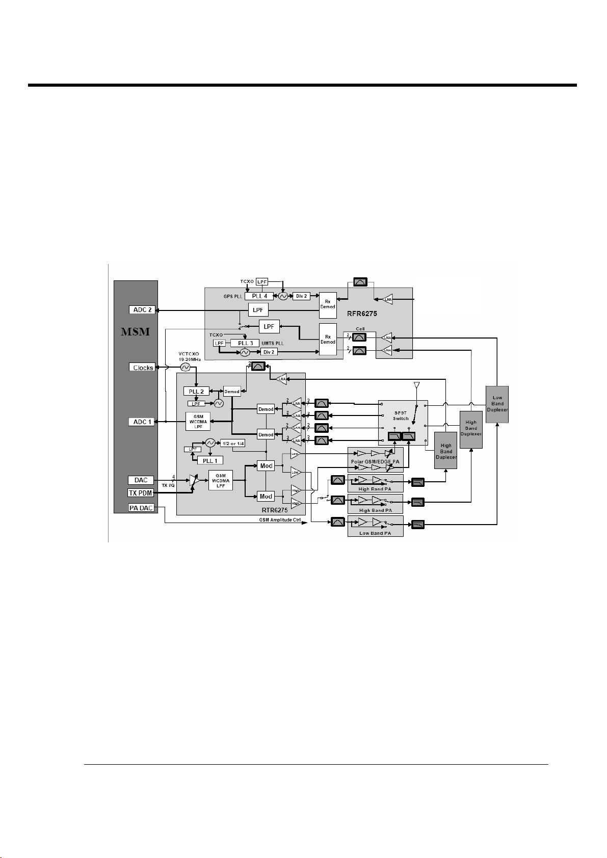
3.1 General Description
The MU515 supports UMTS-850, UMTS-1900, GSM-850, GSM-900, DCS-1800, and PCS-1900 based
GSM/GPRS/EDGE/UMTS. All receivers and the UMTS transmitter use the radioOne1Zero-IF
architecture to eliminate intermediate frequencies, directly converting signals between RF and
baseband. The quad-band GSM transmitters use a baseband-to-IF upconversion followed by an offset
phase-locked loop that translates the GMSK-modulated or 8-PSK-modulated signal to RF.
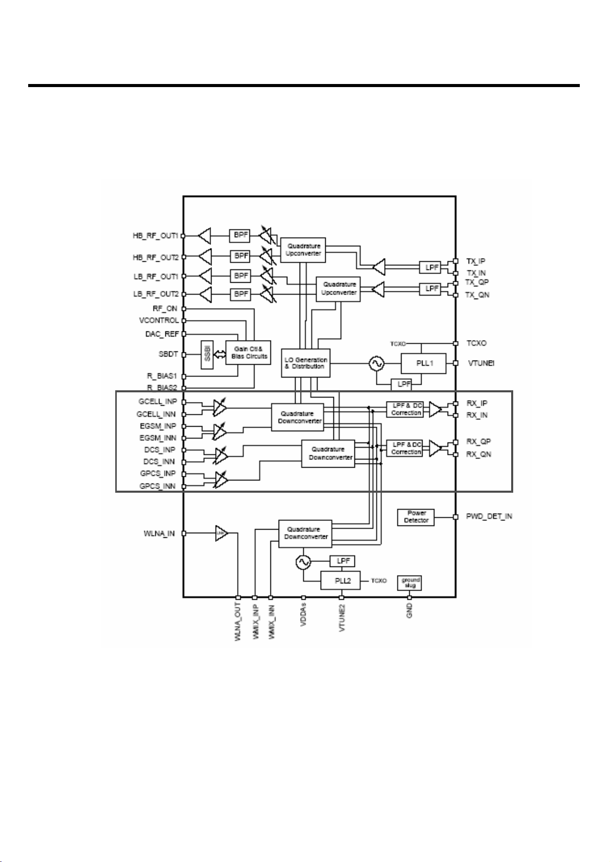
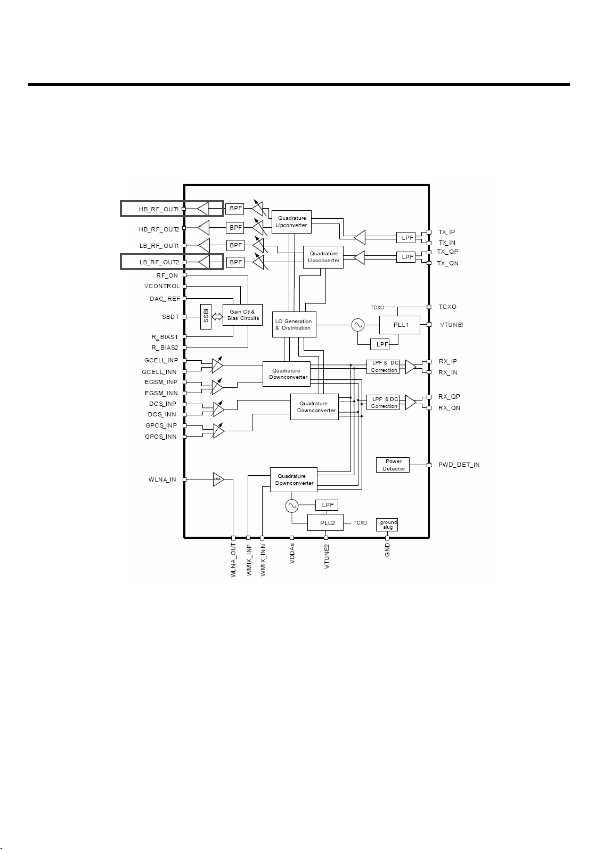
A generic, high-level functional block diagram of MU515 is shown in Figure 1-1. One antenna collects
base station forward link signals and radiates handset reverse link signals. The antenna connects with
receive and transmit paths through a FEM(Front End Module) (plustwo duplexers for UMTS high-band
and low-band operations).
1
QUALCOMM’s branded chipset that implements a Zero-IF radio architecture.
3. TECHNICAL BRIEF
Fig 1.1 Block diagram of RF part

LGE Internal Use Only
Copyright © 2007 LG Electronics. Inc. All right reserved.
Only for training and service purposes
The UMTS receive paths each include an LNA, an RF band-pass filter, and a downconverter that
translate the signal directly from RF-to-baseband using radioOne ZIF techniques. The high-band
UMTS receive path and low-band path are accommodated in the RFR6275 IC. The RFIC.s Rx analog
baseband outputs, for the receive chains, connect to the MSM IC. The UMTS and GSM Rx baseband
outputs share the same inputs to the MSM IC (at ADC1).
For the transmit chains, the RTR6275 IC directly translates the Tx baseband signals (from the MSM
device) to an RF signal using an internal LO generated by integrated on-chip PLL and VCO. The
RTR6275 IC outputs deliver fairly high-level RF signals that are first filtered by Tx SAWs and then
amplified by their respective UMTS PAs. The high- and low-band UMTS RF transmit signals emerge
from the RTR6275 transceiver.
In the GSM receive path, the received RF signals are applied through their band-pass filters and
down-converted directly to baseband in the RTR6275 transceiver IC. These baseband outputs are
shared with the UMTS receiver and routed to the MSM IC for further signal processing. The RFR6275
GSM/UMTS IC receiver baseband outputs share the same interface to the MSM IC input ADC as the
RTR6275 IC baseband outputs.
The GSM/EDGE transmit path employs one stage of up-conversion and, in order to improve efficiency,
is divided into phase and amplitude components to produce an open-loop Polar topology:
1. The on-chip quadrature up-converter translates the GMSK-modulated signal or 8-PSK modulated
signal, to a constant envelope phase signal at RF;
2. The amplitude-modulated (AM) component is applied to the ramping control pin of Polar power
amplifier from a DAC within the MSM
MU515 power supply voltages are managed and regulated by the PM6650 Power Management IC.
This versatile device integrates all wireless handset power management, general housekeeping, and
user interface support functions into a single mixed signal IC. It monitors and controls the external
power source and coordinates battery recharging while maintaining the handset supply voltages using
low dropout, programmable regulators.
The device’s general housekeeping functions include an ADC and analog multiplexer circuit for
monitoring on-chip voltage sources, charging status, and current flow, as well as user-defined off-chip
variables such as temperature, RF output power, and battery ID. Various oscillator, clock, and counter
circuits support IC and higher-level handset functions. Key parameters such as under-voltage lockout
and crystal oscillator signal presence are monitored to protect against detrimental conditions.
3. TECHNICAL BRIEF
- 14 -
LGE Internal Use Only
Copyright © 2007 LG Electronics. Inc. All right reserved.
Only for training and service purposes
3. TECHNICAL BRIEF
- 15 -
3.2 GSM Mode
3.2.1 GSM Receiver
The Dual-mode MU515’s receiver functions are split between the three RFICs as follows:
• UMTS-850,1900 operation uses the RFR6275 Receiver ICs to implement the receive signal path,
accepting an RF input and delivering analog baseband outputs (I and Q).
• GSM-850, GSM-900, DCS-1800, and PCS-1900 modes both use the RTR6275 IC only. Each mode
has independent front-end circuits and down-converters, but they share common baseband circuits
(with only one mode active at a time). All receiver control functions are beginning with SBI2-controlled
parameters.
RF Front end consists of antenna, antenna switch module(DGM099M01) which includes four RX saw
filters(GSM850, GSM900, GSM900, DCS and PCS). The antenna switch module allows multiple
operating bands and modes to share the same antenna. In MU515, a common antenna connects to
one of eight paths: 1) UMTS-850 Rx/Tx, 2) UMTS-1900 Rx/Tx, 3) GSM-850 Rx, 4) GSM-900 Rx, 5)
GSM-850 GSM-900 Tx, (Low Band Tx’s share the same path) 6) DCS-1800 Rx, and 7) DCS1800,PCS-1900 Tx(High Band Tx’s share the same path), 8) PCS-1900 Rx. UMTS operation requires
simultaneous reception and transmission, so the UMTS Rx/Tx connection is routed to a duplexer that
separates receive and transmit signals. GSM850/GSM900, DCS, and PCS operation is time division
duplexed, so only the receiver or transmitter is active at any time and a frequency duplexer is not
required.
2
The RFIC operating modes and circuit parameters are MSM-controlled through the proprietary 3-line Serial Bus Interface (SBI). The Application
Programming Interface (API) is used to implement SBI commands. The API is documented in AMSS Software-please see applicable AMSS
Software documentation for details.
ANT_SEL0 ANT_SEL1 ANT_SEL2
GSM900/GSM850 TX HIGH LOW HIGH
DCS/PCS TX LOW HIGH HIGH
GSM 850 RX LOW LOW LOW
GSM 900 RX HIGH LOW LOW
DCS RX HIGH HIGH LOW
PCS RX LOW HIGH LOW
UMTS 850 LOW HIGH HIGH
UMTS 1900 LOW LOW HIGH
ANTENNA SWITCH MODULE LOGIC
Table 1.1 Antenna Switch Module Control logic
DGM099M01

LGE Internal Use Only
Copyright © 2007 LG Electronics. Inc. All right reserved.
Only for training and service purposes
The GSM850, GSM900, DCS, and PCS receiver inputs of RTR6275 are connected directly to the
transceiver front-end circuits(filters and antenna switch module). GSM850, GSM900, DCS, and PCS
receiver inputs are similar to the RFR6275 UMTS Rx input in that they also use differential
configurations to improve common-mode rejection and second-order nonlinearity performance. The
balance between the complementary signals is critical and must be maintained from the RF filter
outputs all the way into the IC pins
Since GSM850, GSM900, DCS, and PCS signals are time-division duplex (the handset can only
receive or transmit at one time), switches are used to separate Rx and Tx signals in place of frequency
duplexers - this is accomplished in the switch module.
The GSM850, GSM900, DCS, and PCS receive signals are routed to the RTR6275 through band
selection filters and matching networks that transform single-ended 50-Ωsources to differential
impedances optimized for gain and noise figure. Similar to the RFR, the RTR input uses a differential
configuration to improve second-order inter-modulation and common mode rejection performance. The
RTR6275 input stages include MSM-controlled gain
The amplifier outputs drive the RF ports of the quadrature RF-to-baseband downconverters. The
downconverted baseband outputs are multiplexed and routed to lowpass filters (one I and one Q)
having passband and stopband characteristics suitable for GMSK or 8-PSK processing.
These filter circuits include DC offset corrections. The filter outputs are buffered and passed on to the
MSM6260 IC for further processing (an interface shared with the RFR6275 UMTS receiver outputs.
3. TECHNICAL BRIEF
- 16 -
LGE Internal Use Only
Copyright © 2007 LG Electronics. Inc. All right reserved.
Only for training and service purposes
3. TECHNICAL BRIEF
- 17 -
RTR6275 RX feature
LGE Internal Use Only
Copyright © 2007 LG Electronics. Inc. All right reserved.
Only for training and service purposes
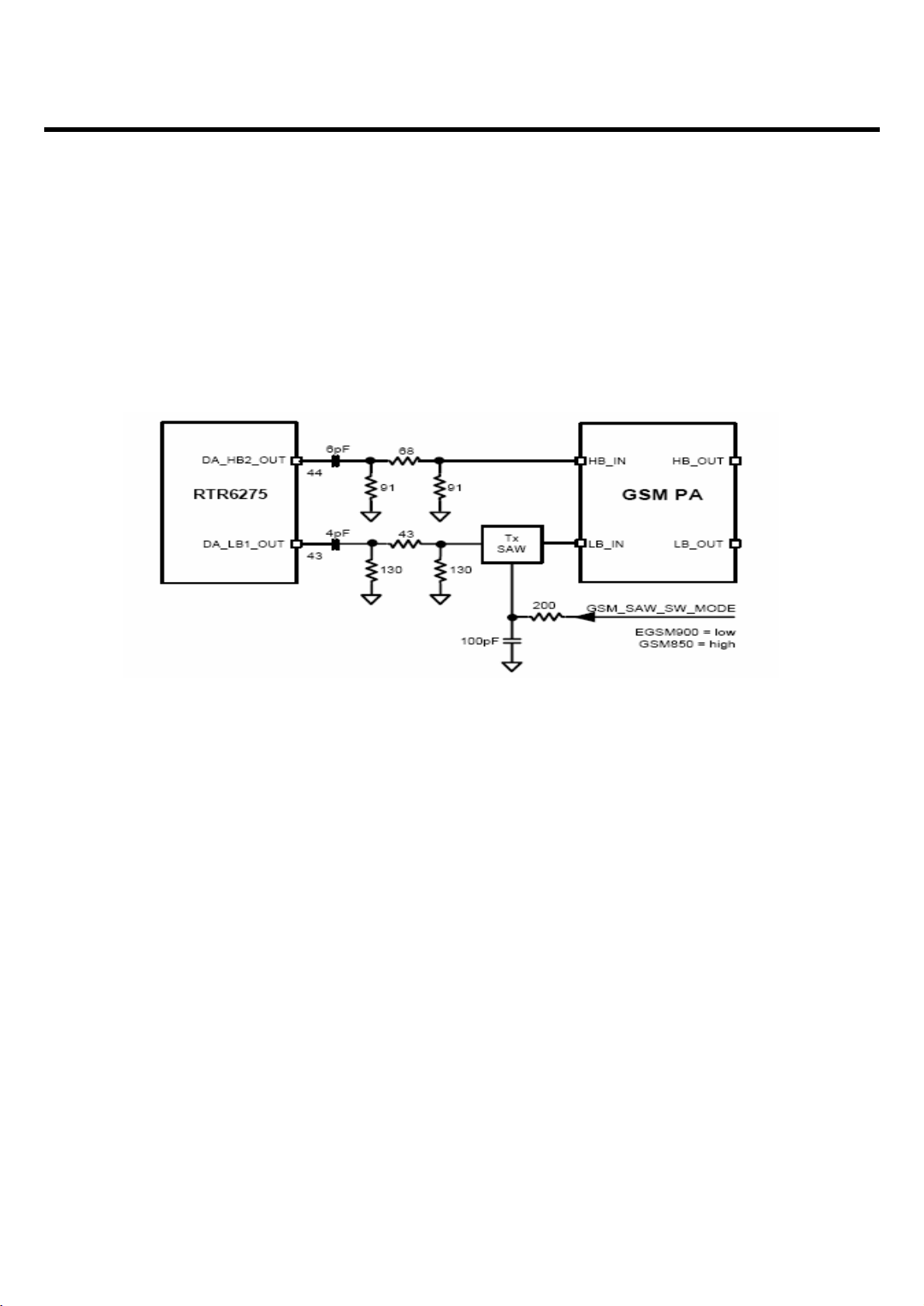
3.2.2 GSM Transmitter out put
The RTR6275 transmitter outputs(DA_HB2_OUT and DA_LB1_OUT)include on-chip output matching
inductors. 50ohm output impedance is achieved by adding a series capacitor at the output pins. The
capacitor value may be optimized for specific applictions and PCB characteristics based on pass-band
symmetry about the band center frequency, the suggested starting value is shown in Figure1.2.
The RTR6275 IC is able to support GSM 850/1900 and GSM 1800/1900 mode transmitting. This design
guideline shows a quad-band GSM application.
Both high-band and low band outputs are followed by resistive pads to ensure that the load Presented
to the outputs remains close to 50ohm. The low-band GSM. Tx path also includes a Tx-band SAW filter
to remove noise-spurious components and noise that would be amplified by the PA and appear in the
GSM Rx band.
3. TECHNICAL BRIEF
- 18 -
Figure 1.2.2-1 GSM Transmitter matching
LGE Internal Use Only
Copyright © 2007 LG Electronics. Inc. All right reserved.
Only for training and service purposes
3. TECHNICAL BRIEF
- 19 -
3.3 UMTS Mode
3.3.1 Receiver
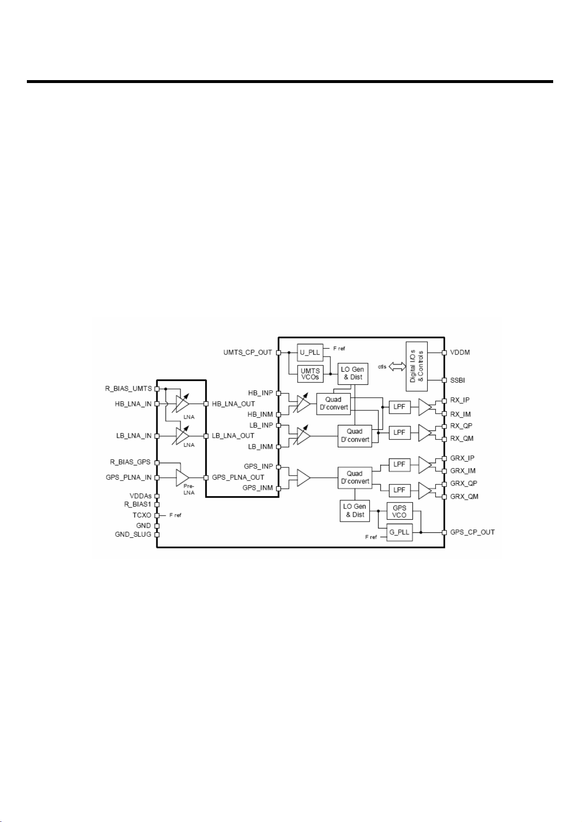
The UMTS duplexer receiver output is routed to LNA circuits within the RFR6275 device.
UMTS LNA circuits(one for low-band UMTS and one for high-band UMTS path) separated from all other
receive functions contained within the RFR6275 reveiver IC to improve mixer LO to RF isolation- a
critical parameter in the ZIF architecture. Isolation is further improved using high-reverse isolation
circuits in the LNA designs. The LNA gains are stepped via API control. The IC operating mode and
LNA bias currents are automatically adjusted via software to minimize DC power consumption.
Figure 1.3.1-1 RFR6275 IC functional block diagram

LGE Internal Use Only
Copyright © 2007 LG Electronics. Inc. All right reserved.
Only for training and service purposes
Separate GPS and UMTS down-converters exist within the RFR6275 to allow GPS signals to be
processed independently of UMTS signals. The inputs use differential configurations to improve
second-order intermodulation and common-mode rejection performance. The differential input gain
stage implements MSM IC-controlled gain adjustments to extend receiver dynamic range.
The outputs of the differential amplifiers drive the RF port of the quadrature RF-tobaseband downconverters. The down-converters are routed to low-pass filters (one I and one Q) whose pass-band and
stop-band characteristics supplement MSM device processing. These filter circuits allow for DC offset
correction and the differential I/Q outputs are buffered to interface with the MSM IC.
. Numerous secondary functions also are integrated on-chip: the Rx LO generation and distribution
circuits and various interface, control, and status circuits. An on-chip UMTS VCO is phase locked to the
external VC-TCXO signal and processed, by the LO generation and distribution circuits, to create the
UMTS Rx LO signals for the quadrature down-converter. A second on-chip GPS VCO is also phaselocked to the VC-TCXO signal to generate the LO signals for the GPS down-converter. The LO signals,
applied to their respective mixer, are at frequencies different to that of the VCOs, which is an important
consideration for ZIF processing. The QUALCOMM MSM device provides status and control signaling,
employing power reduction features (such as selective circuit power-down, gain control, and bias
control) to extend handset standby time.
3.3.2 Transmitter
The UMTS Tx path begins with differential baseband signals (I and Q) from the MSM device. mixers.
The up-converter output is amplified by multiple variable gain stages that provide transmit AGC control.
The AGC output is filtered and applied to the driver amplifier; this output stage includes an integrated
matching inductor that simplifies the external matching network to a single series capacitor to achieve
the desired 50-Ωinterface.
The RTR6275 UMTS output is routed to its power amplifier through a bandpass filter, and delivers fairly
high-level signals that are filtered and applied to the PA. Transmit power is delivered from the duplexer
to the antenna through the switch module.
The transceiver LO synthesizer is contained within the RTR6275 IC with the exception of the off-chip
loop filter components and the VC-TCXO. This provides a simplified design for multimode applications.
The PLL circuits include a reference divider, phase detector, charge pump, feedback divider, and digital
logic generator.
UMTS Tx. Using only PLL1, the LO generation and distribution circuits create the necessary LO signals
for nine different frequency converters. the UMTS transmitter also employs the ZIF architecture to
translate the signal directly from baseband to RF. This requires FLOto equal FRF, and the RTR6275 IC
design achieves this without allowing F
VCO
to equal FRF.
The RTR6275 IC is able to support UMTS 2100/1900 and UMTS 850 mode transmitting. This design
guideline shows only UMTS 2100/1900 and UMTS 850 applications.
3. TECHNICAL BRIEF
- 20 -
LGE Internal Use Only
Copyright © 2007 LG Electronics. Inc. All right reserved.
Only for training and service purposes
3. TECHNICAL BRIEF
- 21 -
RTR6275 IC functional block diagram
LGE Internal Use Only
Copyright © 2007 LG Electronics. Inc. All right reserved.
Only for training and service purposes
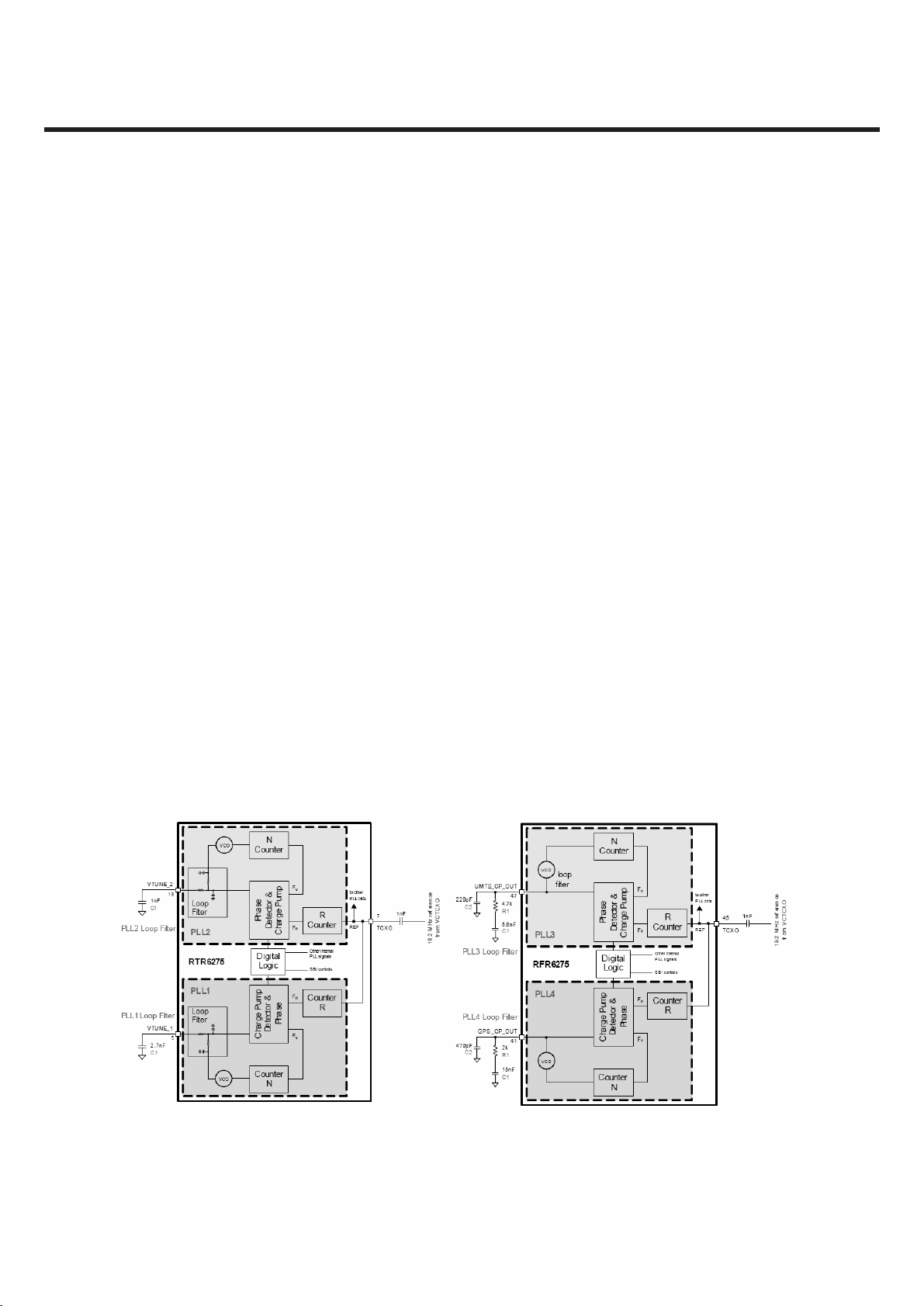
3.4 LO Phase-locked Loop
All LO functions are fully integrated on-chip and do not require user any adjustment. QUALCOMM has
established and implemented frequency plans and LO generation schemes that support the radioOne
Platform B-series chipset. Only one area requires handset designer attention: the loop filters relating to
each PLL. These are addressed in this chapter. All the UMTS Rx, GSM Rx, and GPS PLL circuits are
included within the RFICs: reference dividers, phase detectors, charge pumps, feedback dividers, and
digital logic. There are four integrated VCOs and PLLs within the Platform B (RFCMOS)
chipset as shown in Figure 5-1 and Figure 5-2:
■ Figure 5-1
1. PLL1, within the RTR6275 IC, produces the LO for up- and down-conversion of GSM Tx/Rx, and
UMTS Tx.
2. PLL2, within RTR6275 IC, produces the Rx LO for one of the (high band) UMTS receive Paths.
■ Figure 5-2
3. PLL3, within the RFR6275 IC, produces the Rx LO for the remaining UMTS receive paths.
4. PLL4, within the RFR6275 IC, produces the Rx LO for the GPS receive path.
Within the RFICs, a buffered 19.2 MHz TCXO signal provides the synthesizer input (REF), the
frequency reference to which the PLL is phase- and frequency-locked. Thereference is divided by the
R-Counters to create a fixed frequency input to the phase detector, FR. The other phase detector input
(FV) varies as the loop acquires lock, and is generated by dividing the VCO frequency using the
feedback path N-Counter. The closed loop will force FV to equal FR when locked. If the loop is not
locked, the error between FV and FR will create an error signal at the output of the charge pump. This
error signal is filtered by the loop filter components and applied to the VCO, tuning the output
frequency so that the error is decreased. Ultimately, the loop forces the error to approach zero and the
PLL is phase- and frequency-locked.
3. TECHNICAL BRIEF
- 22 -
RFR6275 PLLs functional block diagram
Figure 5-1 Figure 5-2
LGE Internal Use Only
Copyright © 2007 LG Electronics. Inc. All right reserved.
Only for training and service purposes
3. TECHNICAL BRIEF
- 23 -
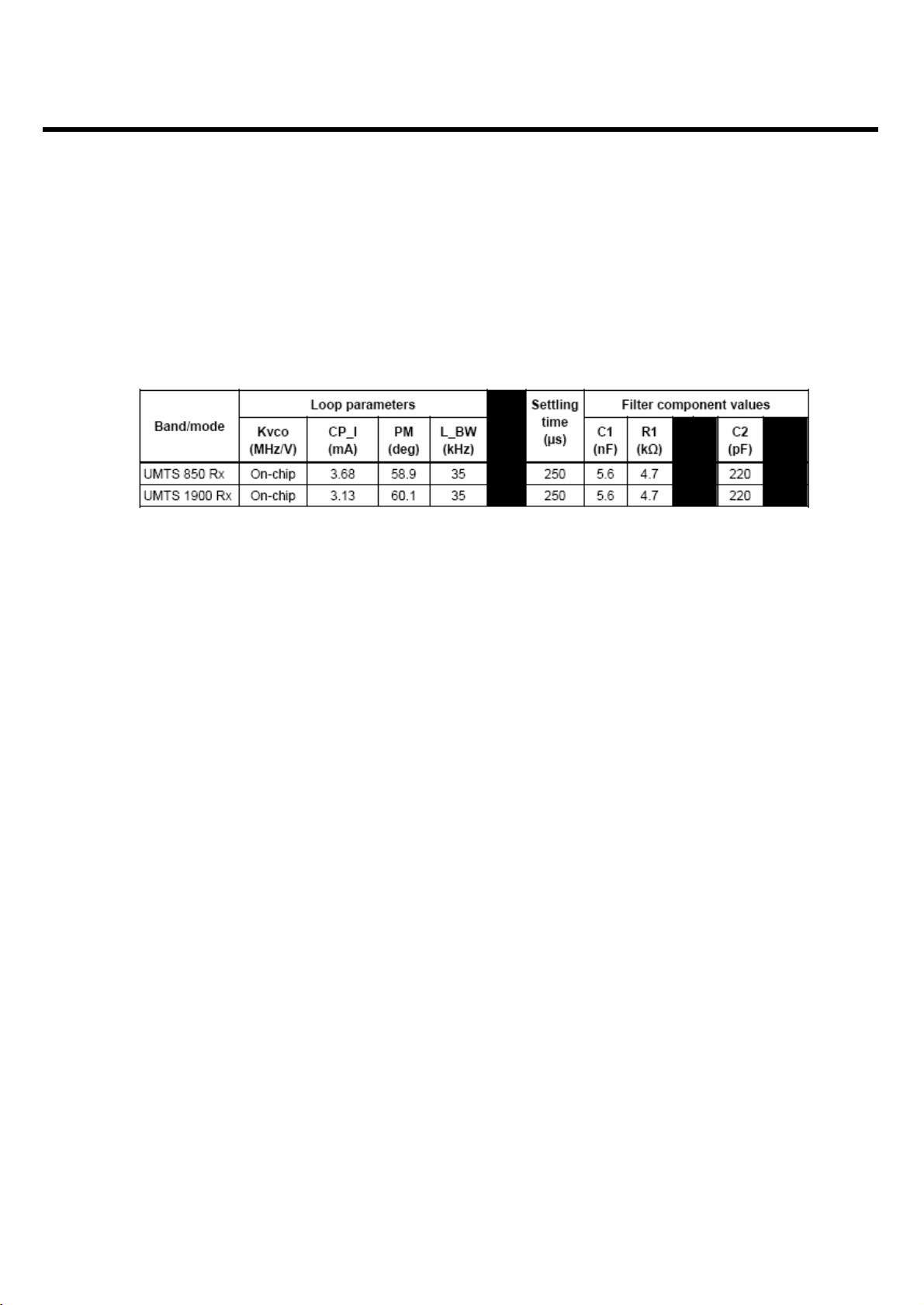
3.4.1 UMTS Rx PLL (PLL3)
QUALCOMM provides a baseline PLL3 design for UMTS Rx. Loop filter component reference
designators are shown in Figure 5-2.
Table_ Baseline PLL3 design for UMTS Rx
Notes: 1. The performance values listed in this table are based on simulation results and are provided
as a starting point for handset designers. Synthesizer performance is still being evaluated
and optimized during this document release. Loop parameter, settling time, and filter
component values are all expected to change when the optimization effort is completed.
Future revisions will include expected performance based on measured data.
2. For MU515 C1_2.2nF C2_150pF R1_10k
3. Loop parameter acronyms are: Kvco VCO tuning sensitivity CP_I Charge pump current
(controlled by API software) PM Phase margin L_BW Loop bandwidth
4. The listed VCO tuning sensitivity is based on QUALCOMM internal Rx VCO.
5. The listed settling times are for switching between channels at opposite ends of the active
band and settling to within 250 Hz of the final frequency.
6. Test and evaluation efforts were ongoing at the time of this document release. Check future
versions for design recommendations based on our test results.
3.4.2 Transceiver PLL (PLL1)
The PLL1 within the RTR6275 IC creates the Rx LO for all the GSM receive bands and GSM transmit
bands as well as the UMTS transmit bands. The PLL1 of RTR6275 IC (with on-chip VCO) creates the
transceiver LO that supports the quad-band GSM receivers and the GSM transmitters as well as the
tri-band UMTS transmit outputs. All LO functional blocks are integrated into the RTR6275 IC except for
some loop filter capacitors (Figure 5-1). On-chip circuits include reference divider, phase detector,
charge pump, VCO, feedback divider, and digital logic status. The off-chip loop filter capacitors allow
minimal optimization of PLL performance characteristics (stability, transitory response, settling time,
and phase noise) for different applications.
LGE Internal Use Only
Copyright © 2007 LG Electronics. Inc. All right reserved.
Only for training and service purposes
3.5 Off-chip RF Components
3.5.1 Antenna switch module
3. TECHNICAL BRIEF
- 24 -

LGE Internal Use Only
Copyright © 2007 LG Electronics. Inc. All right reserved.
Only for training and service purposes
3. TECHNICAL BRIEF
- 25 -
3.5.2 UMTS duplexer
A UMTS duplexer splits a single operating band into receive and transmit paths. Important
performance requirements include;
■ Insertion loss . this component is also in the receive and transmit paths ; In the MU515 typical losses
: UMTS1900_ Tx = 2.1 dB, UMTS1900_ Rx = 2.8 dB and UMTS850_ Tx =1.9 dB, UMTS850_ Rx =
2.7 dB
■ Out-of-band rejection or attenuation . the duplexer provides input selectivity for the receiver, output
filtering for the transmitter, and isolation between the two. Rejection levels for both paths are
specified over a number of frequency ranges. Two Tx-to-Rx isolation levels are critical to receiver
performance:
■ Rx-band isolation . the transmitter is specified for out-of-band noise falling into the Rx band. This
noise leaks from the transmit path into the receive path, and must be limited to avoid degrading
receiver sensitivity. The required Rx-band isolation depends on the PA out of-band noise levels and
Rx-band losses between the PA and LNA. Minimum duplexer Rx band isolation value is about 45
dB.
■ Tx-band isolation . the transmit channel power also leaks into the receiver. In this case, the leakage
is outside the receiver passband but at a relatively high level. It combines with Rx band jammers to
create cross-modulation products that fall in-band to desensitize the receiver. The required Tx-band
isolation depends on the PA channel power and Tx-band losses between the PA and LNA. Minimum
duplexer Tx-band isolation value is about 55 dB.
■ Passband ripple . the loss of this fairly narrowband device is not flat across its passband. Passband
ripple increases the receive or transmit insertion loss at specific frequencies, creating performance
variations across the band.s channels, and should be controlled.
■ Return loss . minimize mismatch losses with typical return losses of 10 dB or more (VSWR <2:1).
■ Power handling . high power levels in the transmit path must be accommodated without degraded
performance. The specified level depends on the operating band class and mobile station class (per
the applicable standard), as well as circuit losses and antenna EIRP. Several duplexer
characteristics depend upon its source and load impedances. QUALCOMM strongly recommends
an isolator be used between the UMTS PA and duplexer to assure proper performance.
LGE Internal Use Only
Copyright © 2007 LG Electronics. Inc. All right reserved.
Only for training and service purposes
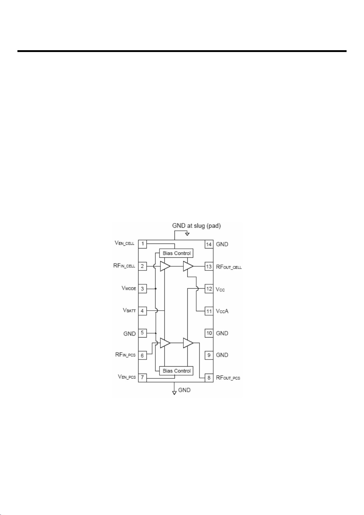
3.5.3 UMTS Power Amplifier
UMTS850/UMTS1900 Power Amplifier module.
The AWT6321 addresses the demand for increased integration in dual-band handsets for North
American CDMA network deployments. The small footprint 3 mm x 5 mm x 1 mm surface mount RoHS
compliant package contains independent RF PA paths to ensure optimal performance in both
frequency bands, while achieving a 25% PCB space savings compared with solutions requiring two
single-band PAs. The package pinout was chosen to enable handset manufacturers to easily route
VCC to both power amplifiers and simplify control with a common VMODE pin. The device is
manufactured on an advanced InGaP HBT MMIC technology offering state-of-the-art reliability,
temperature stability, and ruggedness. The AWT6321 is part of ANADIGICS’ High- Efficiency-at-LowPower (HELPTM) family of CDMA power amplifiers, which deliver low quiescent currents and
significantly greater efficiency without a costly external DAC or DC-DC converter.
3. TECHNICAL BRIEF
- 26 -
Block Diagram
LGE Internal Use Only
Copyright © 2007 LG Electronics. Inc. All right reserved.
Only for training and service purposes
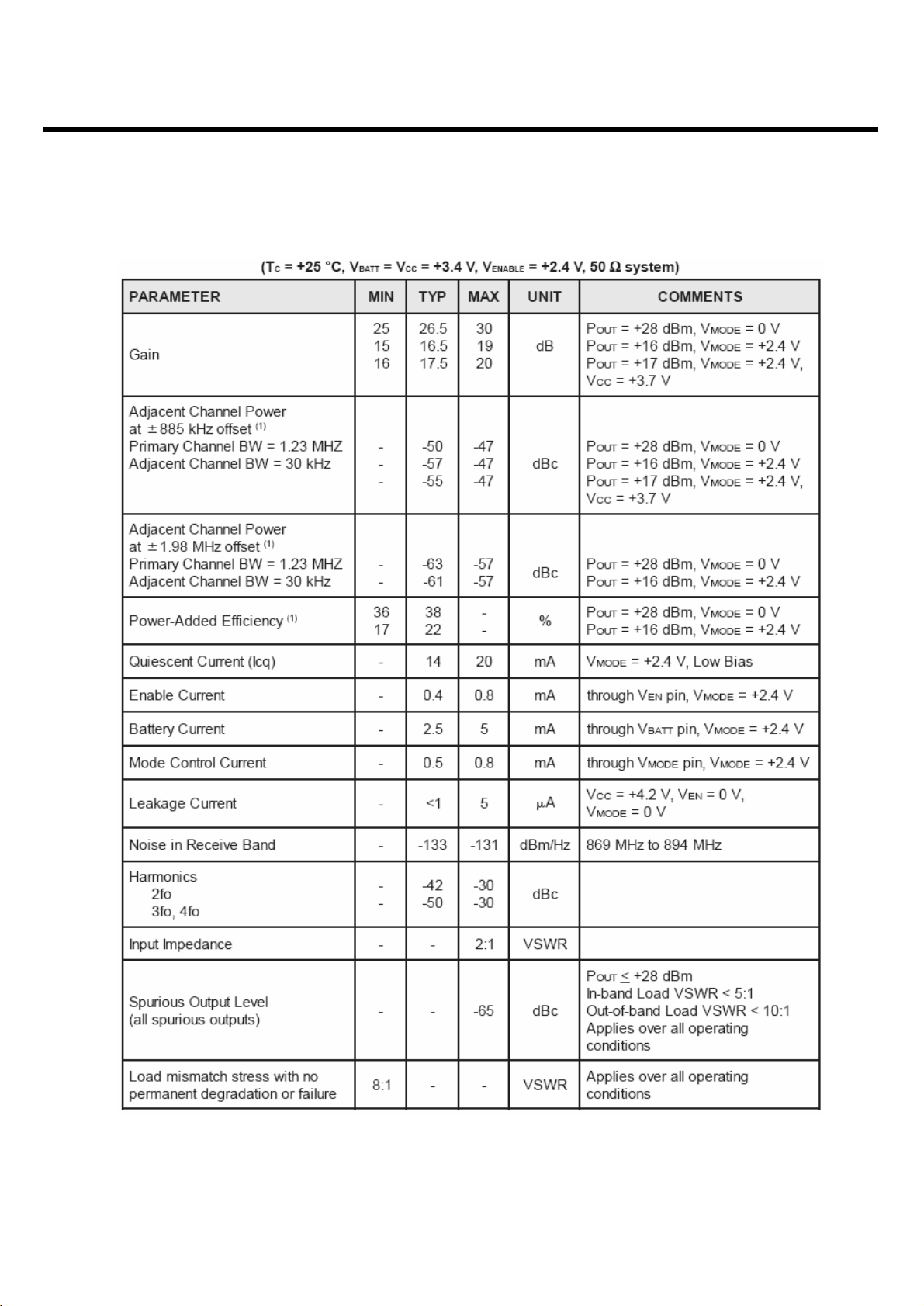
3. TECHNICAL BRIEF
- 27 -
Electrical specifications-Cellular Band
LGE Internal Use Only
Copyright © 2007 LG Electronics. Inc. All right reserved.
Only for training and service purposes
3. TECHNICAL BRIEF
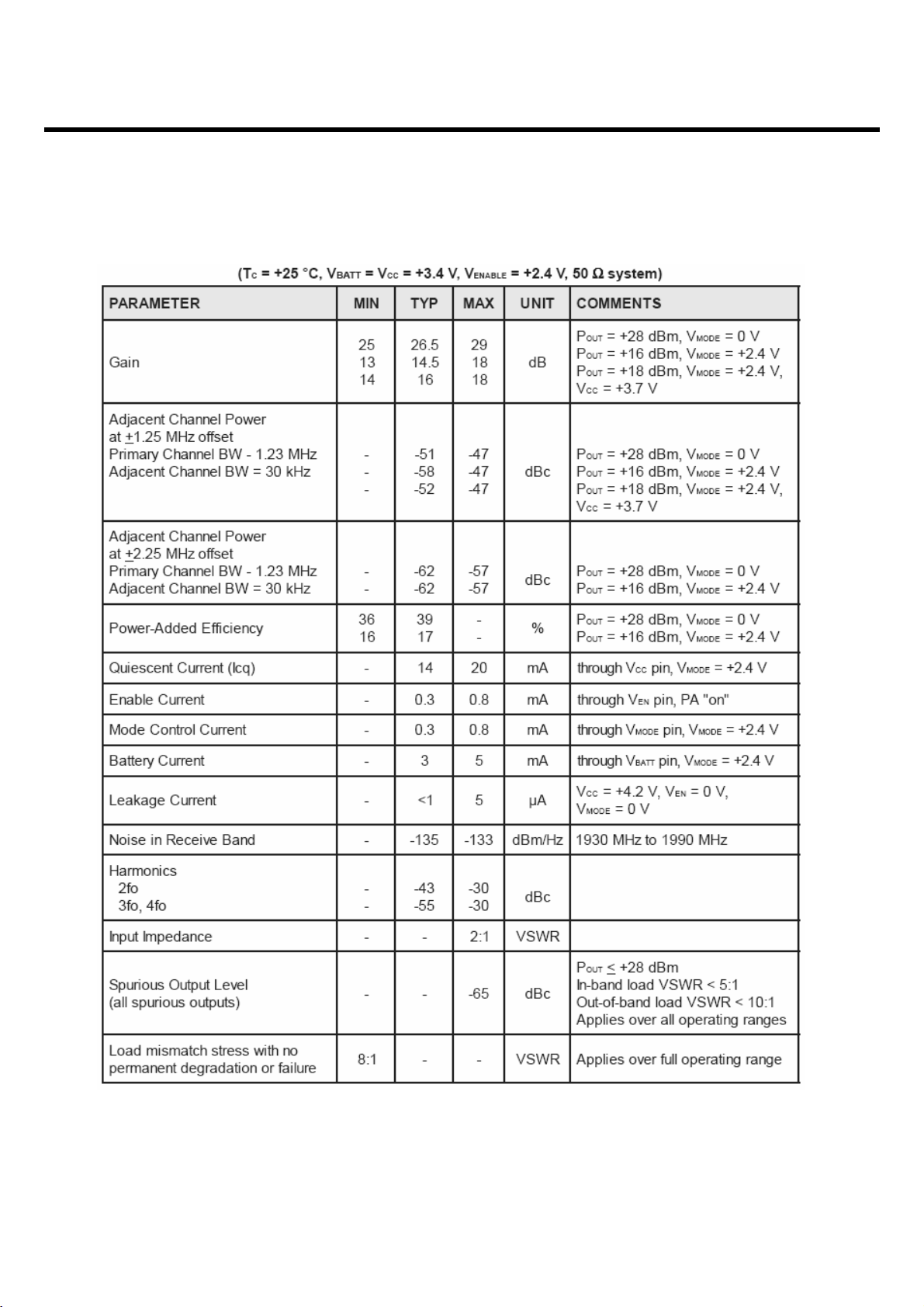
- 28 -
Electrical specifications - PCS Band
LGE Internal Use Only
Copyright © 2007 LG Electronics. Inc. All right reserved.
Only for training and service purposes
3. TECHNICAL BRIEF
- 29 -
3.5.4 Thermistor
This thermistor senses temperature variations around UMTS PA to adjust PA gain deviation for assure
compliance with the applicable transmit power control standards. Negative temperature compensation
thermistor is used in the MU515.
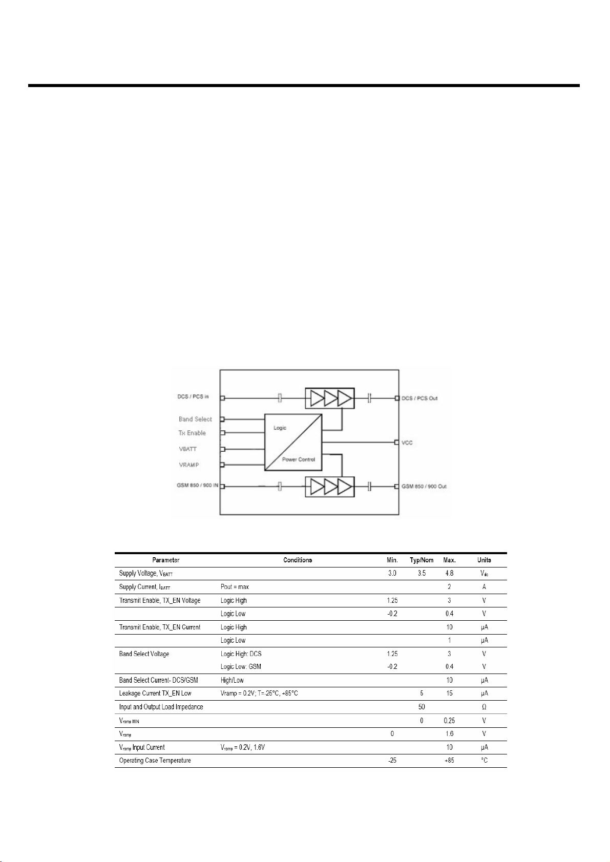
3.5.5 GSM/GPRS/EDGE Power amplifier
Product Description
The TQM7M5003 is a small (7x7mm), GSM/EDGE PAM for handset applications. This module has
been optimized for excellent EDGE efficiency, ACPR and EVM in an open loop polar modulation
environment at EDGE class E2+ operation while maintaining high GSM/GPRS efficiency. The
TQM7M5003 is fan-out compatible with TriQuint’s other power amplifier modules.
GSM PA functional block diagram
Operating Parameter

- 30 -
3. TECHNICAL BRIEF
3.5.6 UMTS Rx RF filter
Filter1 869 ~ 894MHz Filter2 1805 ~1880MHz
An RF filter is located between the UMTS LNA and mixer. Insertion loss is important, but not as critical
as losses before the LNA. The most important parameters of this component include:
■ Out-of-band rejection or attenuation levels, usually specified to meet these conditions:
❑ Far out-of-band signals - ranging from DC up to the first band of particular concern and from the
last band of particular concern to beyond three times the highest passband frequency.
❑ Tx-band leakage - the transmitter channel power, although attenuated by the duplexer, still
presents a cross-modulation threat in combination with Rx-band jammers. The RF filter must
provide rejection of this Tx-band leakage.
❑ Other frequencies of particular concern . bands known to include other wireless transmitters that
may deliver significant power levels to the receiver input.
■ Phase and amplitude balance - the ZIF architecture requires well-balanced differential inputs to the
RFR6202 IC. This is accomplished by the RF filter which takes a single-ended output from the
RFL6202 IC and provides differential outputs having nominal 180° phase separation. Phase and/or
amplitude imbalance causes degraded common-mode rejection and second-order nonlinearity, so
their requirements are specified jointly.
❑ ±3 degrees and ± 1 dB
❑ -12 to + 3 degrees and ± 0.7 dB
Of course, passband ripple and return loss are still important in all cases for the same reasons
explained in the antenna switch module and duplexer sections.
3.5.7 VCTCXO
The Voltage Controlled Temperature Compensated Crystal Oscillator (VCTCXO) provides the
reference frequency for all RFIC synthesizers as well as clock generation functions within the
MSM6260 IC. The oscillator frequency is controlled by the MSM6260’s TRK_LO_ADJ pulse density
modulated signal in the same manner as the transmit gain control.
The filtered PDM signal results in an analog control signal into the VCTCXO tuning port whose voltage
is directly proportional to the density of the digital bit stream. The MSM device varies the pulse density
to change the analog control voltage that sets the oscillator frequency - all within a feedback control
loop that minimizes handset frequency drift relative to the network.
LGE Internal Use Only
Copyright © 2007 LG Electronics. Inc. All right reserved.
Only for training and service purposes
- 31 -
3. TECHNICAL BRIEF
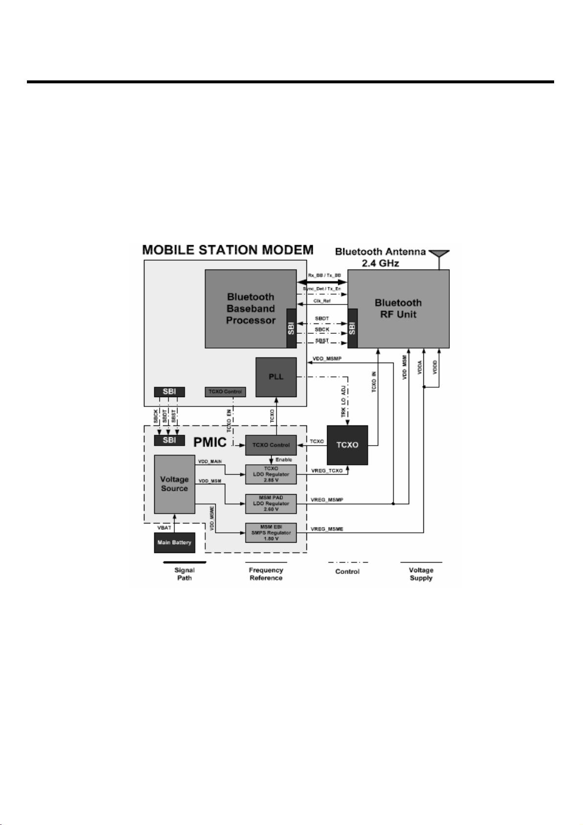
3.5.8 Bluetooth
The MSM6260 includes BT baseband embedded BT 1.1 compliant baseband core, so the other
bluetooth components are an bluetooth RF module and Antenna. Figure1.5.12-1 shows the
bluetooth system architecture in the MU515.
LGE Internal Use Only
Copyright © 2007 LG Electronics. Inc. All right reserved.
Only for training and service purposes
Figure1.5.12-1 Bluetooth system architecture
 Loading...