

Page 1

960L
Multi-Channel
Digital Effects System
Service
Manual
Page 2
960L Multi-Channel Digital Effects System Service Manual
Copyright © 1999 Lexicon, Inc.
All Rights Reserved
Lexicon Inc. ● 3 Oak Park ● Bedford, MA 01730-1441 ● Tel (781) 280-0300 ● Customer Service Fax (781) 280-0499
Lexicon Part # 070-14826 Rev 0
Printed in the United States of America
Page 3

960L Multi-Channel Digital Effects System Service Manual
Page 4
960L Multi-Channel Digital Effects System Service Manual
Page 5

Lexicon
Table of Contents
Chapter 1 Reference Documents, Required Equipment............................. 1-1
Reference Documents............................................................................................................................. 1-1
Required Equipment................................................................................................................................ 1-1
Tools .................................................................................................................................................... 1-1
Test Equipment.................................................................................................................................... 1-1
Chapter 2 General Information ................................................................... 2-1
Periodic Maintenance .............................................................................................................................. 2-1
Ordering Parts ......................................................................................................................................... 2-1
Returning Units to Lexicon for Service .................................................................................................... 2-1
Chapter 3 Specifications............................................................................. 3-1
960L Mainframe....................................................................................................................................... 3-1
LARC2 User Interface ............................................................................................................................. 3-3
Chapter 4 Performance Verification............................................................ 4-1
Initial Inspection and checkout: ............................................................................................................... 4-1
960L Mainframe: .................................................................................................................................. 4-1
LARC2 controller:................................................................................................................................. 4-1
Cables:................................................................................................................................................. 4-1
Power Supplies: ................................................................................................................................... 4-1
Audio/Functional Tests Setup*: ............................................................................................................... 4-5
I/O Gain Tests ......................................................................................................................................... 4-6
Analog In to Analog Out Audio Gain Test: ........................................................................................... 4-6
Analog In To Digital Out Audio Gain Test: ........................................................................................... 4-6
Digital Input to Analog Output Gain Test:............................................................................................. 4-6
Frequency Response: ............................................................................................................................. 4-6
Analog In to Analog Out Frequency Response Test:........................................................................... 4-6
Analog In To Digital Out Frequency Response Test:........................................................................... 4-6
Digital In To Analog Out Frequency Response Test:........................................................................... 4-7
THD+N Measurement:............................................................................................................................. 4-7
Analog In to Analog Out THD+N Test:................................................................................................. 4-7
Analog In to Digital Out THD+N Test: .................................................................................................. 4-7
Digital In to Analog Out THD+N Test: .................................................................................................. 4-7
Crosstalk Tests:....................................................................................................................................... 4-8
Analog In to Digital Out Crosstalk Test: ............................................................................................... 4-8
Digital In to Analog Out Crosstalk Test: ............................................................................................... 4-8
Dynamic Range Tests: ............................................................................................................................ 4-8
Analog In to Analog Out Dynamic Range Test: ................................................................................... 4-8
Analog In to Digital Out Dynamic Range Test:..................................................................................... 4-8
Digital In To Analog Out Dynamic Range Test: ................................................................................... 4-8
Functional Tests: ..................................................................................................................................... 4-9
Midi Tests:............................................................................................................................................ 4-9
Listening Test:...................................................................................................................................... 4-9
Lexicon Audio Precision ATE Summary ............................................................................................ 4-11
Chapter 5 Service Notes............................................................................. 5-1
Motherboard - lithium battery................................................................................................................... 5-1
Power Supplies........................................................................................................................................ 5-1
Symptoms of possible power supply failures ....................................................................................... 5-1
Larc2 Meter Display LED Handling ......................................................................................................... 5-1
Removal and Replacement of Larc2 Piezo Transducer .......................................................................... 5-1
For units with the transducer soldered (Rev 5 PCB and up):............................................................... 5-1
For units with the transducer epoxied (Rev 4 PCB and below):........................................................... 5-1
Female RS-422 Wraparound Plug: ......................................................................................................... 5-3
Male RS-422 Wraparound Plug............................................................................................................... 5-4
Page 6

960L Multi-Channel Digital Effects System Service Manual
Chapter 6 Troubleshooting ......................................................................... 6-1
Diagnostics...............................................................................................................................................6-1
Overview...............................................................................................................................................6-1
960L Diagnostics: .................................................................................................................................6-1
960L Diagnostic User Interface: ...........................................................................................................6-2
Audio I/O Algorithm (8 In - 8 Out): ........................................................................................................6-3
Functional Diagnostic Test Scripts .......................................................................................................6-3
960L Setup for Functional Diagnostic Tests .........................................................................................6-4
960L Power On Diagnostic Descriptions: .............................................................................................6-4
960L Functional Diagnostic Descriptions:.............................................................................................6-5
960L Troubleshooting Tools: ..............................................................................................................6-16
Global Commands: .............................................................................................................................6-17
LISTING of RESIDENT SCRIPTS ......................................................................................................6-18
LARC2 DIAGNOSTICS ..........................................................................................................................6-24
Debug Port:.........................................................................................................................................6-25
POWER ON DIAGNOSTICS:.................................................................................................................6-26
Power On Diagnostics Sequence: ......................................................................................................6-26
Power On Self Tests:..........................................................................................................................6-28
INTERACTIVE DIAGNOSTICS:.............................................................................................................6-33
Self Test:.............................................................................................................................................6-34
LCD Test:............................................................................................................................................6-35
Key Test:.............................................................................................................................................6-35
LED Test:............................................................................................................................................6-36
Joystick Test: ......................................................................................................................................6-38
Fader/Motor Test: ...............................................................................................................................6-39
Lexicon Test: ......................................................................................................................................6-39
Memory Test:......................................................................................................................................6-40
Repetitive Test:...................................................................................................................................6-40
Diagnostics Suite: ...............................................................................................................................6-41
OPTION BOARD Menu:.........................................................................................................................6-42
MISCELLANEOUS TESTS:................................................................................................................6-44
Program Flash Data Checking:...........................................................................................................6-46
Chapter 7 Theory of Operation ................................................................... 7-1
NLX Backplane.........................................................................................................................................7-1
Overview...............................................................................................................................................7-1
Circuit Description.................................................................................................................................7-1
NLX Interface (Sheet1) .........................................................................................................................7-2
PCI Interface (Sheets 2, 3, 4) ...............................................................................................................7-2
IO Connectors (Sheet 5).......................................................................................................................7-2
Miscellaneous Connectors (Sheet 6)....................................................................................................7-2
IOBUS & Power Connectors (Sheet 7).................................................................................................7-2
DSPBUS Connectors (Sheet 8, 9)........................................................................................................7-3
I/O Backplane...........................................................................................................................................7-4
Introduction ...........................................................................................................................................7-4
Overview...............................................................................................................................................7-4
Circuit Description.................................................................................................................................7-5
I/O Clock card - Input/Output and Clock Generator card..........................................................................7-7
Midi Interface ........................................................................................................................................7-7
Ttl Wordclock Interface .........................................................................................................................7-7
Larc2 Interface......................................................................................................................................7-8
CPLD Logic...........................................................................................................................................7-8
Control Interface .................................................................................................................................7-10
Register Descriptions..........................................................................................................................7-10
Access ................................................................................................................................................7-10
Description .............................................................................................................................................7-10
Page 7

Lexicon
Board ID ................................................................................................................................................ 7-10
Interface revision ................................................................................................................................... 7-10
Preview Word Clock Select ................................................................................................................... 7-10
Clock Bus Interface............................................................................................................................ 7-10
Clock Selection .................................................................................................................................. 7-11
PLL Support ....................................................................................................................................... 7-11
Phase-Locked Loop ........................................................................................................................... 7-11
PLL Detailed Description ................................................................................................................... 7-12
Power Supply..................................................................................................................................... 7-14
Analog Input card .................................................................................................................................. 7-15
Overview. ........................................................................................................................................... 7-15
Input Buffer ........................................................................................................................................ 7-15
Common Mode Performance............................................................................................................. 7-15
A/D Converter .................................................................................................................................... 7-16
Signal Polarity .................................................................................................................................... 7-16
System Interface Logic ...................................................................................................................... 7-16
Control Interface ................................................................................................................................ 7-16
Register Descriptions......................................................................................................................... 7-16
Clock Interface ................................................................................................................................... 7-17
Digital Audio Interface........................................................................................................................ 7-17
Pin Descriptions ................................................................................................................................. 7-18
Power Supply..................................................................................................................................... 7-20
Analog Output card................................................................................................................................ 7-21
Overview............................................................................................................................................ 7-21
Circuit Description.............................................................................................................................. 7-21
D/A Converter .................................................................................................................................... 7-21
Filter................................................................................................................................................... 7-22
Output Driver...................................................................................................................................... 7-22
Mute Relay......................................................................................................................................... 7-22
Signal Polarity .................................................................................................................................... 7-23
System Interface Logic ...................................................................................................................... 7-23
Control Interface ................................................................................................................................ 7-23
Register Descriptions......................................................................................................................... 7-23
Clock Interface ................................................................................................................................... 7-23
Digital Audio Interface........................................................................................................................ 7-24
Power Supply..................................................................................................................................... 7-26
AES card ............................................................................................................................................... 7-28
Introduction ........................................................................................................................................ 7-28
Overview............................................................................................................................................ 7-28
Circuit Description.............................................................................................................................. 7-29
Startup Sequence .............................................................................................................................. 7-29
AES card Memory Map...................................................................................................................... 7-29
FPGA Control Register ...................................................................................................................... 7-30
FPGA Lock Register .......................................................................................................................... 7-30
Locking to the AES Input Word Clock................................................................................................ 7-31
Octal Select Register ......................................................................................................................... 7-31
Local Loopback Mode:....................................................................................................................... 7-32
Reverb card ........................................................................................................................................... 7-32
Introduction ........................................................................................................................................ 7-32
Overview............................................................................................................................................ 7-32
Circuit Description.............................................................................................................................. 7-33
Startup Sequence .............................................................................................................................. 7-36
DSP 56301 Expansion Port Memory Map ......................................................................................... 7-37
Larc2...................................................................................................................................................... 7-39
General Description ........................................................................................................................... 7-39
Central Processor (sheet 1) ............................................................................................................... 7-40
Page 8

960L Multi-Channel Digital Effects System Service Manual
Main Memory (sheet 2).......................................................................................................................7-41
Peripheral I/O Subsystems .................................................................................................................7-44
Power Supply......................................................................................................................................7-49
Register Summary ..............................................................................................................................7-50
Meter Bridge Module ..........................................................................................................................7-53
Chapter 8 - Parts List.................................................................................. 8-1
CHASSIS/MECHANICAL .........................................................................................................................8-1
I/O BPL ASSY,960L .................................................................................................................................8-2
I/O CLK BD ASSY,960L ...........................................................................................................................8-3
AIN BD ASSY,960L..................................................................................................................................8-4
AOUT BD ASSY,960L..............................................................................................................................8-5
AES BD ASSY,960L.................................................................................................................................8-7
RVB BD ASSY,960L ................................................................................................................................8-8
NLX CPU BD ASSY .................................................................................................................................8-9
NLX BPL EXT BD ASSY,960L .................................................................................................................8-9
I/O BPL EXT BD ASSY,960L ...................................................................................................................8-9
LARC2:...................................................................................................................................................8-10
CHASSIS/MECHANICAL: ..................................................................................................................8-10
SHIP MAT’L/PACKAGING/MISCELLANEOUS ..................................................................................8-14
POWER CORDS....................................................................................................................................8-14
SHIP MAT’L/PACKAGING/MISCELLANEOUS......................................................................................8-14
Spare Assemblies ..................................................................................................................................8-15
Chapter 9 Schematics and Drawings ......................................................... 9-1
Schematics:..............................................................................................................................................9-1
Drawings: .................................................................................................................................................9-1
Page 9

Lexicon
Chapter 1 Refe rence Documents, Required Equipment
Reference Documents
960L Owner's Manual - Lexicon P/N 070-14353 or latest revision
Software Release Notice, 960L - Lexicon P/N 070-14354 or latest revision
Required Equipment
Tools
The following is a minimum suggested technician's tool kit required for performing disassembly, assembly
and repairs:
• Clean, antistatic, well lit work area.
• (1) #1 Phillips tip screwdriver
• (1) #2 Phillips tip screwdriver
• Small pair chain nose pliers
• Solder: 63/37 - Tin/Lead Alloy composition, low residue, no-clean solder.
• Magnification glasses and lamps
• SMT Soldering / Desoldering bench-top repair station
Test Equipment
The following is a minimum suggested equipment list required for performing the proof of performance and
diagnostic tests.
• Digital Multi-Meter ( DMM )
• Amplifier with speakers or headphones.
• Cables: (dependent on your signal source)
• low distortion analog oscillator
• analog distortion analyzer and level meter with Audio Band-Pass filter
• 100 MHz oscilloscope
• digital distortion analyzer & digital function generator (e.g. Stanford Research Systems Model DS360 or
Audio Precision System 1 with DSP Option/System 2).
• Variable AC Power Supply with voltage and current meters,(known as a Variac), adjustable from 0 -
140VAC, and 0-2Amps.BK Precision 1653 or equivalent.
• 100/120 to 220/240 VAC step-up transformer
• LARC2 to 960L Interface Cable, Lexicon P/N 680-03525.
• (2) Male D9 RS422 Wraparound Connectors (see Chapter 5 for spec/drawing)
• (2) audio cables XLR male on one end with appropriate connectors on the opposite end for connection
to the low distortion oscillator.
• (2) audio cables XLR female on one end with appropriate connectors on the opposite end for
connection to a headphone amplifier.
• Stereo Headphones
• XLR male to XLR female audio cables, maximum length 1 meter.
• XLR male to XLR female audio cables, maximum length 2 meters.
• BNC to BNC Cables, maximum length 5 meters.
• XLR male to XLR female 110 ohm AES digital audio cables, maximum length 1 meter.
• (8) XLR male to XLR female 110 ohm AES digital audio cables, maximum length 2 meters.
• (2) 5 Pin DIN to 5 Pin DIN Cables, maximum length 3 meters, (MIDI Cables), Hosa Technology P/N
MID-305 or equivalent.
• Lexicon 960L PCI Extender cards P/N 023-14297
• Lexicon 960L I/O Extender cards P/N 023-14426
• 960L 120V Power Cord, Lexicon P/N 680-09149
1-1
Page 10

960L Multi-Channel Digital Effects System Service Manual
• IBM compatible personal computer capable of running Windows 95/98, minimum 200mHz Pentium
Processor, 128MB memory, 4GB Hard Disk Drive, SVGA Monitor, Video card w/ 4MB memory, Mouse,
17” monitor, Windows 95 Keyboard, CD-ROM Drive, 3.5" High Density Floppy Disk Drive, and Windows
95/98 Operating System.
• 6' DE-9 Female to DE-9 Female RS-232 Serial Cable.
• DE-9 Male to DE-9 Male RS-232 Null-Modem Adapter
• Female RS-422 Wraparound Plug (see Chapter 5 for spec/drawing)
• PS/2 Keyboard (or IBM 102/104-key keyboard with PS/2 adapter)
• Optional:
• High Current Continuity Tester, 10A, 100 milliohm. Associated Research 5030DT or
equivalent.
• (1) 15” Computer Monitor
• (1) PS/2 Mouse
• LARC2 Option Board (Rev.1), Lexicon P/N 023-14310.
• 32MB PCMCIA FLASH Memory Card, PCMCIA 2.1 Compliant, 5 Volt, (LINEAR Flash
PC Card, Centennial P/N FL32M-20-11736-J5).
• External Power Supply, 12VDC @ 3A, 5.5 mm O.D., 2.5 mm I.D. barrel connector, with
the positive voltage on center contact. PowDec Model WI60-12V or equivalent.
Page 11

Lexicon
Chapter 2 Gene ral Information
Periodic Maintenance
Under normal conditions the 960L system requires minimal maintenance. Use a soft, lint-free cloth slightly
dampened with warm water and mild detergent to clean the exterior surfaces.
Do not use alcohol, benzene or acetone-based cleaners or any strong commercial cleaners. Avoid
using abrasive materials such as steel wool or metal polish. It the unit is exposed to a dusty environment, a
vacuum or low-pressure blower may be used to remove dust from the unit's exterior.
The 960L's cooling fan, located on the right side of the mainframe (facing the front) has a removable filter. It
should be cleaned periodically with water and mild detergent, rinsed thoroughly, dried and reinstalled.
Ordering Parts
When ordering parts, identify each part by type, price and Lexicon Part Number. Replacement parts can be
ordered from:
LEXICON, INC.
3 Oak Park
Bedford, MA 01730-1441
Telephone: 781-280-0300; Fax: 781-280-0499; email: csupport@lexicon.com
ATTN: Customer Service
Returning Units to Lexicon for Service
Before returning a unit for warranty or non-warranty service, consult with Lexicon Customer
Service to determine the extent of the problem and to obtain Return Authorization. No equipment
will be accepted without Return Authorization from Lexicon.
If Lexicon recommends that a 960L be returned for repair and you choose to return the unit to Lexicon for
service, Lexicon assumes no responsibility for the unit in shipment from the customer to the factory,
whether the unit is in or out of warranty. All shipments must be well packed (using the original packing
materials if possible), properly insured and consigned, prepaid, to a reliable shipping agent.
When returning a unit for service, please include the following information:
• Name
• Company Name
• Street Address
• City, State, Zip Code, Country
• Telephone number (including area code and country code where applicable)
• Serial Number of the unit
• Description of the problem
• Preferred method of return shipment
• Return Authorization #, on both the inside and outside of the package
Please enclose a brief note describing any conversations with Lexicon personnel (indicate the name of the
person at Lexicon) and give the name and telephone daytime number of the person directly responsible for
maintaining the unit.
Do not include accessories such as manuals, audio cables, footswitches, etc. with the unit, unless
specifically requested to do so by Lexicon Customer Service personnel.
2-1
Page 12

Page 13

Chapter 3 Spec ifications
960L Mainframe
Analog Input
Connectors Eight, Female XLR
Impedance 50Kohm, balanced
Level (for 0 dbFS) +24dBu
Freq Response @48K 20Hz-20KHz, ±1db
Freq Response @96K 20Hz-40KHz, ±1db
A/D Conversion 24 bits
128x oversampled
A/D Dyn Range >110 dB (20-20kHz)
THD <.002%
CMRR >50db
Crosstalk @ 1Khz < -100dB
Analog Output
Connectors Eight, Male XLR
Impedance 50 Ohm, balanced
Level (at 0 dbFS) +24dBu
Freq Response @48K 20Hz-20Khz, ±1db
Freq Response @96K 20Hz-40Khz, ±1db
D/A Conversion 24 bits
8x oversampled @ 44.1/48Khz
4x oversampled @ 88.2/96Khz
Lexicon
D/A Dyn Range >110 dB (20-20kHz)
THD <.002%
Crosstalk @ 1Khz < -100dB
A/A Performance
Freq Response @48K 20Hz-20Khz, ±1db
Freq Response @96K 20Hz-40Khz, ±1db
Dyn Range >107 dB (20-20kHz)
THD <.002%
Digital Audio IO
Connectors Four Male XLR Outputs
Four Female XLR Inputs
Format AES/EBU
Word Size 24 bits
Sample Rates
Internal 44.1/48/88.2/96KHz
Accuracy within ±10ppm
External 44.1/48/88.2/96KHz
Lock Range ±1%
Group Delays (milliseconds)
3-1
Page 14

960L Multi-Channel Digital Effects System Service Manual
A/D
A/A 2.42 2.23 1.80 1.66
D/A 1.54 1.42 1.35 1.25
D/D 0.54 0.50 0.36 0.33
Synchronization
TTL Word Clock Input *
75 Ohm, BNC
self-terminating loopthru
TTL Word Clock Output * Low Z, BNC
(* Falling edge marks start of frame)
Clock Jitter
Intrinsic Exceeds AES3 Amendment 1
Jitter Gain Exceeds AES3 Amendment 1
Control Interfaces
LARC2 Ports 2
MIDI ** In/Out/Thru
(**supports program change)
Algorithms
Ambience (48K Stereo & Surround)
Chamber (48K Stereo & Surround)
Plate (48K Stereo & Surround)
Reverse (48K Stereo & Surround)
Random Hall
(48/96K Stereo & 48K Surround)
Ambient Chamber (48K Surround)
44.1
Khz
1.44 1.33 0.81 0.74
48
Khz
88.2
Khz
96
Khz
Standard Hardware Configuration
DSP/CPU Card Compartment
One System CPU Card
One Reverb DSP Card
Two Spare DSP card slots
One MIDI Card
IO Card Compartment
One Analog Input Card
One Analog Output Card
One AES/EBU Digital IO Card
One IO/Clock Card
One Spare IO Card slot
Storage Media
Hard Disk
3.5” Floppy Disk Drive
CD-ROM Drive
Reverb Card Configurations
48K
Page 15

Stereo Machines Four
2in x 5out Machines Two
5in x 5out Machines Two
96K
Stereo Machines Two
2in x 5out Machines One
5in x 5out Machines One
Internal Hard Disk Storage
Factory Programs 240
User Registers 1000
Removable 3.5” Floppy Disk Storage
User Registers 100
Power
Requirements***
100-120 / 220-240 VAC
50-60Hz, 300W max
(some mainframes will have a mains voltage selection
switch; if there is no selector switch, it will operate
on mains voltages from 100-240 VAC)
Connector 3-pin IEC
Lexicon
Dimensions
Rack Units 4U
Size 19.0" L x 7.0" W x 17.4" H
(483mm x 178mm x 442mm)
Weight
Regulatory Approvals
FCC Class A
CE EN55103-1, EN55103-2
UL UL1419
cUL C22.2
TUV EN60065
Environment
Operating 10 to 40 °C
Storage -30 to 70 °C
Humidity 95% max, non-condensing
LARC2 User Interface
Display
Type Passive Matrix LCD
Resolution 640x240
Colors 256
Backlight Fluorescent
Contrast HW controlled (rear panel)
Brightness SW controlled
35 lbs
LED Meter Bridge
Configuration 8 channels x 3 levels
Levels
-60dBFS (Signal)
3-3
Page 16

960L Multi-Channel Digital Effects System Service Manual
-6dBFS
-0.5dBFS (Overload)
Control Surface
Faders 8
60mm throw, motorized, touch sensitive
Joystick Two axis
Dedicated Function Keys 29 (12 backlit)
Soft Buttons 8
Connectors
960L 9-pin D-sub
Aux. PS/2 Keyboard 6-pin Mini-DIN
Ext. Power concentric, 2.5mm
Operating Distance
With power from 960L up to100 feet
With Ext. Power up to1000 feet
Power
Requirements 12 VDC, 3 A (max)
Dimensions
Size 12.7” L x 8.25” W x 5.0” H
(323mm x 210mm x 127mm)
Weight 4 lbs
Regulatory Approvals
FCC Class A
CE EN55103-1, EN55103-2
TUV EN60065
Environment
Operating 5 to 40 °C
Storage -30 to 70 °C
Humidity 95% max, non-condensing
Page 17

Lexicon
Chapter 4 Perfo rmance Verification
This section describes the tests and procedures for verification of the operation of the 960L with LARC2
and the integrity of its analog and digital audio signal paths.
Initial Inspection and checkout:
Note: Please refer to the chassis assembly drawing in the Schematics and Drawings section later in this
manual.
960L Mainframe:
1. Remove the top and bottom covers of the 960L
2. Inspect the entire unit for obvious signs of physical damage.
3. Unscrew the front panel screws and fold down the front panel.
4. Verify that the main processor board, midi card, and reverb cards are seated properly and are held
down with screws. Also verify that all cable connections to the midi card, main processor board, and
backplanes are in place.
5. At the back of the unit, in the power supply section, verify that all connections are firmly seated to the
backplane. Verify all ribbon cables are firmly seated to the I/O backplane and that Pin 1 of all ribbon
cables (identified by a red stripe) are at the top of the connectors.
6. Carefully turn the unit over.
7. Verify that all of the drives are properly secured in place. Verify all ribbon cables and power cables to
these devices are firmly seated.
8. Verify all ribbon cables to both the NLX and I/O backplanes are firmly seated.
9. On the back panel of the 960L make sure all cards are tightly screwed in place. Inspect all connectors
for wear or breaks that might cause intermittent operation.
LARC2 controller:
1. Inspect the entire unit for obvious signs of physical damage such as cracked or broken plastic
housings.
2. Verify display is not cracked or shattered.
3. Verify all sliders move up and down smoothly and do not bind.
4. Verify the joystick also has a smooth, fluid movement.
5. Depress all the buttons to insure non-stick operation.
Cables:
Inspect both the 960L power cable and LARC cable for physical damage or excessive wear.
Power Supplies:
Note: It is important that the power supply be tested while fully connected in the 960L mainframe
to insure proper voltage readings.
System Current Draw Tests:
1. For 100/120V operation, verify that the voltage selection switch* on the back of the 960L is set to the
115 Volt setting.
2. Set the voltage level on the Variable AC power supply down to 0 volts then turn it ON.
3. Plug the 960L into the variable AC power supply and switch the main power switch on the rear panel to
the ON position.
4. Slowly bring the variable AC power supply voltage up to 120 Volts. The current draw will vary from
between approximately 0.5A and 1.5A.
5. At 120V verify that the current draw is approximately 0.75 A and that the Green Power On LED above
the Front Panel power switch is on.
6. Power off.
4-1
Page 18
960L Multi-Channel Digital Effects System Service Manual
7. For 220/240V operation, verify that the voltage selection switch* on the back of the 960L is set to the
230 Volt setting.
8. Follow steps 2 through 6 above. Note - the current draw should be approximately one-half of that listed
in the steps above dependant upon the accuracy of the current meter. It should not be higher.
*Note: Different manufacturer's power supplies have been specified for the 960L. There are some slight
mechanical differences in some of these power supplies. Some units will have a power supply with a
voltage setting switch as noted above. Some units will have a power supply that does not have a voltage
selection switch. The AC voltage input will be automatically sensed by the supply. Be sure to inspect the
unit in case of the need to "switch" for the appropriate AC input voltage.
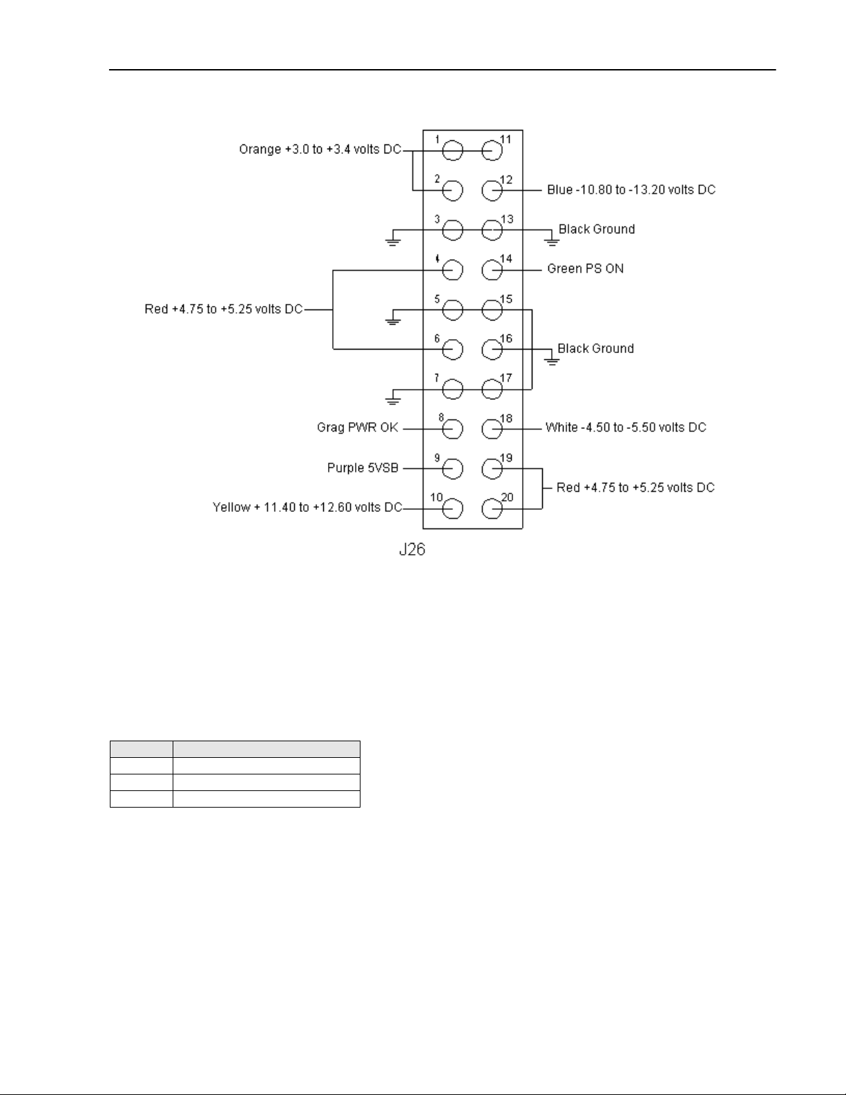
Main Power Supply Connector J26 Voltage Level Tests:
1. Remove the top and bottom covers of the 960L.
2. Remove all DSP cards and the Midi card from the card cage in the front section of the 960L and place
them in static shielding bags.
3. With the front of the 960L facing you, locate the solder side of connector J26 on the Left side of the NLX
backplane.
4. Clip the ground lead of the DMM meter to the chassis for ground reference.
5. Take the Plus lead and using the table below verify the voltage levels indicated on J26.
Pin # Wire Color Voltage Range
1 Orange + 3 volts DC +.4/-0
4 Red + 5 volts DC ±.25
10 Yellow + 12. volts DC ±.6
12 Blue -12 volts DC ±1.2
13 Black Ground
18 White - 5 volts DC ±.5
4-2
Page 19
Lexicon
NOTE: The following voltage tests are to insure that the connectors are plugged into the NLX
backplane and that power is being properly distributed to the other devices. This may also help in
determining whether or not the devices themselves are defective.
To gain easier access to the test points called out in the following tests, you will want to turn over the
mainframe of the 960L so the bottom faces up or rest it on its side.
All power connections to the backplane, Hard Drive, CD ROM Drive and 3.5" Floppy Drive have the same
colored wiring code.
Color Voltage Range
Yellow + 12. volts DC ±.6
Black Ground
Red + 5 volts DC ±.25
NLX Backplane Connector J9 Voltage Level Test:
1. Locate the power connector J9 on the rear backplane.
2. Measure the voltages on the connector with your DMM leads.
3. Place the DMM ground lead on the Black wire connector and the DMM plus lead on the Yellow wire
connector and verify the voltage is +12 VDC (± .6 VDC).
4. Place the DMM ground lead on the Black wire connector and the DMM plus lead on the Red wire
connector and verify the voltage is + 5 VDC (± .25 VDC).
3.5" Floppy Drive Connector:
1. Locate the power connector on the back of 3.5” Floppy Drive.
2. With your DMM leads measure the voltages on the connector.
4-3
Page 20

960L Multi-Channel Digital Effects System Service Manual
3. Place the DMM ground lead on the Black wire connector and the DMM plus lead on the Yellow wire
connector and verify the is +12 VDC (± .6 VDC).
4. Place the DMM ground lead on the Black wire connector and the DMM plus lead on the Red wire
connector and verify the voltage is +5 VDC (± .25 VDC).
CD-ROM Drive Connector:
1. Locate the power connector on the back of CD-ROM drive.
2. With your DMM leads measure the voltages on the connector.
3. Place the DMM ground lead on the Black wire connector and the DMM plus lead on the Yellow wire
connector and verify the voltage is +12 VDC (± .6 VDC).
4. Place the DMM ground lead on the Black wire connector and the DMM plus lead on the Red wire
connector and verify the voltage is +5 VDC (± .25 VDC).
Hard Drive Connector:
1. Locate the power connector on the back of Hard Drive.
2. With your DMM leads measure the voltages on the connector.
3. Place the DMM ground lead on the Black wire connector and the DMM plus lead on the Yellow wire
connector and verify the voltage is +12 VDC (± .6 VDC).
4. Place the DMM ground lead on the Black wire connector and the DMM plus lead on the Red wire
connector and verify the voltage is +5 VDC (± .25 VDC).
For the following voltage tests, an I/O extender card (part # 023-14426) will be needed to bring the cards
out of the mainframe in order to gain access to the test points called out in the following tests.
Analog Output Card Voltage Test:
The supplies being tested on this card will be the +/-12 VSUP, and the +5VD provided by the main supply
via the backplane and voltages +5VD, 6.6V, +/-18V, 24V, and 36V created on the card.
1. Before powering on the 960L for this test, remove the Analog Output card from the rear of the chassis.
2. Insert the I/O extender card and install the Analog Output card into the extender card.
3. Power on the 960L.
4. For your ground reference locate test point marked GND to the Left of U3.
5. At the back right hand corner of the card locate the –12V-test point just below FB2. Verify the voltage is
-12VDC ±1.2VDC.
6. Next locate in the test point marked +12V just below FB3. Verify the voltage is +12VDC ±.6VDC.
7. Locate the +5VD voltage test point left side of the card just above U6. Verify the voltage is +5VDC
±.25VDC.
8. Locate the +5 VA voltage test point just below U3 between D8 and D9. Verify the voltage is +5VDC
±.25VDC.
9. Locate the + VB voltage test point on the right side of the card just to the left of C15. Verify the voltage
is between + 6.27 and + 6.93 VDC.
10. Locate the +/- VCC voltage test points on the right side of the card. +VCC is just to the right of C206
and –VCC is just to the right of that under FB54. Verify the voltage to be +17.50VCC and -17.50VCC
+/- 1.0 volt each.
Analog Input Card Voltage Test:
The supplies being tested on this card will be the +/- 12 VSUP provided by the main supply via the
backplane and the +5VD, and +5VA created on the card.
1. Before powering on the 960L for this test, remove the Analog Input card from the rear of the chassis.
2. Insert the I/O extender card and install the Analog Input card into the extender card.
3. Power on the 960L.
4. For your ground reference, locate test point marked GNDA just above D7.
4-4
Page 21

Lexicon
5. At the back right hand corner of the card locate the FB1. Measure the +12 volts here and verify the
voltage is +12VDC ± .6VDC.
6. Next locate FB2. Measure the -12 volts here and verify the voltage is -12VDC ± 1.2VDC.
7. Using the same ground reference measure pin 3 of U3 (+ 5 VA). Verify the voltage is +5VDC ± .25VDC.
8. Locate the + 5 VD test point on the left side of the card just to the left of U1. Using the ground reference
marked GNDD2 just to the right of the + 5 VD verify the voltage is +5VDC ± .25VDC.
AES Input /Output Card Voltage Test:
The supply being tested on this card will be the +5VD provided by the main supply via the backplane.
1. Before powering on the 960L remove the AES Input/Output card from the rear of the chassis.
2. Insert the I/O extender card and install the AES Input/Output card into the extender card.
3. Power on the 960L.
4. Locate the ground reference test point marked GND1 just above U3.
5. Locate test point marked + 5 V to the right of the GND1 test point.
6. With the DMM verify the voltage is +5VDC ± .25VDC.
Input/Output Clock Generator Card Voltage Test:
The supplies being tested on this card will be the +/-12 VSUP and the +5VD provided by the main supply
via the backplane.
1. Before powering on the 960L remove the Input/Output Clock card from the rear of the chassis.
2. Insert the I/O extender card and install the Input/Output Clock card into the extender card.
3. Power on the 960L.
4. For a ground reference locate test point marked GND2 on the right side of the card.
5. Locate the ferrite bead FB3 at the back of the card just to the right of the connector and measure the
+12 volts. Verify the voltage is +12VDC ± .6VDC.
6. FB4 is next to FB3. Measure the -12 volts here. Verify the voltage -12VDC ± 1.2VDC.
7. Locate the ground reference test point marked GND1 on the left side of the card just to the left of U1.
8. Locate test point marked + 5 V just below U1.
9. With the DMM verify the voltage is +5VDC ± .25VDC.
Audio/Functional Tests Setup*:
1. Power on the 960L with the main power switch and wait for the Power on diagnostics cycle to finish.
2. On the Larc2, press the Control Button. The Control Mode screen will appear at this time.
3. Press the #1 button to set the clock source to Internal. Note: for any "Digital In" tests, you will need to
return to this screen and select Source #3, AES/EBU.
4. Press the Right arrow button to jump to the Rate page.
5. Press the #2 button to select a 48kHz sample rate.
6. Press the Soft button labeled CONFIG under the display.
7. Press the #4 button. This will highlight the 1-8in/8out setup for Diagnostics.
8. Press the Edit button, the screen will then display the Edit Mode page
9. Press the Soft button labeled Algorithm, the display will then read Algorithms Options Enabled.
10. Press the Soft button labeled Select, a small box will open with 1-OctalThru stated.
11. Press the #1 button, then the Enter button this will load the Diagnostic 1-8in/8out setup.
12. Press Control and then the ►key to highlight Inputs.
13. Press the + key to toggle the state to AN (Analog). Note: for any "Digital In" tests, you will need to
return to this screen and toggle the state to AES (Digital).
14. Set the distortion analyzer to measure VRMS.
*Note: The following tests should also be performed at the 44.1kHz and 96kHz sample rates. Prior to
performing the following tests at each sample rate, you must perform the previous set-up procedure
substituting the indicated sample rate in step 5.
4-5
Page 22

960L Multi-Channel Digital Effects System Service Manual
I/O Gain Tests
Analog In to Analog Out Audio Gain Test:
1. Connect a balanced XLR audio cable between the low distortion oscillator and the 960L # 1 Audio
Input.
2. Connect a balanced XLR audio cable between the 960L # 1 Audio Output and the distortion analyzer.
3. Apply a 1kHz sinewave @ 9.75 VRMS.
4. Verify the output level to be 10 VRMS ±1.5V.
5. Repeat the test on the remaining Input /Outputs 2-8.
Analog In To Digital Out Audio Gain Test:
1. Connect a balanced XLR audio cable between the low distortion oscillator and the 960L # 1 Audio
Input.
2. Connect a balanced XLR audio cable between the 960L # 1-2 AES Output and the digital distortion
analyzer.
3. Apply a 1kHz sinewave @ 10.94 VRMS.
4. Verify the output level to be -1 dBFS ± 1dBFS.
5. Move the audio input cable to the # 2 Input and repeat the test.
6. Repeat the test on the remaining Input /Outputs pairs 3-4, 5-6, and 7-8.
Digital Input to Analog Output Gain Test:
Note: Change the Clock Source and Inputs to AES - see Audio/Functional Tests Setup.
1. Connect a balanced XLR audio cable between the digital function generator and the 960L # 1-2 AES
Input.
2. Connect a balanced XLR audio cable between the 960L # 1 Audio Output and the distortion analyzer.
3. Apply a 1kHz sinewave @ -1 dBFS.
4. Verify the output level to be 11.5 VRMS ±1.5V.
5. Move the audio output cable to the # 2 Output and repeat the test.
6. Repeat the test on the remaining Input /Outputs pairs 3-4, 5-6, and 7-8.
Frequency Response:
Analog In to Analog Out Frequency Response Test:
Note: Change the Clock Source to Internal and Inputs to Analog - see Audio/Functional Tests Setup.
1. Disable all filters on the distortion analyzer.
2. Connect a balanced XLR audio cable between the low distortion oscillator and the 960L # 1 Audio
Input.
3. Connect a balanced XLR audio cable between the 960L # 1 Audio Output and the distortion analyzer.
4. Apply a 1kHz sinewave @ 2.45 VRMS.
5. Set the Analyzer for a 0dB reference (@1khz)
6. Sweep the oscillator from 20Hz to 20kHz and verify the level is +/- 1dBr throughout the sweep.
7. Repeat the test on the remaining Input /Outputs 2-8.
Analog In To Digital Out Frequency Response Test:
1. Disable all filters on the digital distortion analyzer.
2. Connect a balanced XLR audio cable between the low distortion oscillator and the 960L # 1 Audio
Input.
3. Connect a balanced XLR audio cable between the 960L # 1-2 AES Output and the digital distortion
analyzer.
4. Apply a 1kHz sinewave @ 6.90 VRMS.
5. Set the Analyzer for a 0dB reference (@1khz)
6. Sweep the oscillator from 20Hz to 20kHz and verify the level is +/- 1dBr throughout the sweep.
4-6
Page 23

Lexicon
7. Move the Audio Input cable to Audio Input #2 and repeat the test.
8. Repeat the test on the remaining Input /Outputs pairs 3-4,5-6, and 7-8.
Digital In To Analog Out Frequency Response Test:
Note: Change the Clock Source and Inputs to AES - see Audio/Functional Tests Setup.
1. Disable all Filters on the distortion analyzer
2. Connect a balanced XLR audio cable between the digital function generator and the 960L # 1-2 AES
Input.
3. Connect a balanced XLR audio cable between the 960L # 1 Audio Output and the distortion analyzer.
4. Apply a 1kHz sinewave @ -1 dBFS.
5. Set the Analyzer for a 0dB reference (@1khz)
6. Sweep the oscillator from 20Hz to 20kHz and verify the level is +/- 1dBr throughout the sweep.
7. Move the audio output cable to the # 2 Output and repeat the test.
8. Repeat the test for the remaining Input /Outputs pairs 3-4,5-6, and 7-8.
THD+N Measurement:
Analog In to Analog Out THD+N Test:
Note: Change the Clock Source to Internal and Inputs to Analog - see Audio/Functional Tests Setup.
1. Connect a balanced XLR audio cable between the low distortion oscillator and the 960L # 1 Audio
Input.
2. Connect a balanced XLR audio cable between the 960L # 1 Audio Output and the distortion analyzer.
3. Apply a 997Hz sinewave @ 9.75 VRMS.
4. Set the distortion analyzer to measure THD+N.
5. Enable the Audio Band Pass filter on the distortion analyzer.
6. Verify the output THD+N on the Analyzer is < 0.002%.
7. Repeat the rest for the remaining Input /Outputs 2-8.
Analog In to Digital Out THD+N Test:
1. Connect a balanced XLR audio cable between the low distortion oscillator and the 960L # 1 Audio
Input.
2. Connect a balanced XLR audio cable between the 960L # 1-2 AES Output and the digital distortion
analyzer.
3. Apply a 997Hz sinewave @ 10.94 VRMS.
4. Set the distortion analyzer to measure THD+N.
5. Enable the Audio Band Pass filter on the distortion analyzer.
6. Verify the output THD+N on the Analyzer is < -94 dBFS.
7. Move the audio input cable to the # 2 Input and repeat the test.
8. Repeat the test for the remaining Input /Outputs pairs 3-4,5-6, and 7-8.
Digital In to Analog Out THD+N Test:
Note: Change the Clock Source and Inputs to AES - see Audio/Functional Tests Setup.
1. Connect a balanced XLR audio cable between the digital function generator and the 960L # 1-2 AES
Input.
2. Connect a balanced XLR audio cable between the 960L # 1 Audio Output and the distortion analyzer.
3. Apply a 997Hz sinewave @ -1 dBFS.
4. Set the distortion analyzer to measure THD+N.
5. Enable the Audio Band Pass filter on the distortion analyzer.
6. Verify the output THD+N on the Analyzer is < -94 dBFS.
7. Move the audio output cable to the # 2 Output and repeat the test.
8. Repeat the test for the remaining Input /Outputs pairs 3-4,5-6, and 7-8.
4-7
Page 24

960L Multi-Channel Digital Effects System Service Manual
Crosstalk Tests:
Analog In to Digital Out Crosstalk Test:
1. Connect a balanced XLR audio cable between the low distortion oscillator and the 960L # 1 Audio
Input.
2. Connect a balanced XLR audio cable between the 960L # 1-2 AES Output and the digital distortion
analyzer.
3. Apply a 997Hz sinewave @ 10.94 VRMS.
4. Enable the Audio Band Pass filter on the distortion analyzer.
5. Verify the level on AES Output #2 to be < -100 dB throughout the sweep.
6. Move the Input cable to the # 2 Input and repeat the test for AES Output #1.
7. Repeat the test for the remaining Input /Outputs pairs 3-4, 5-6, and 7-8.
Digital In to Analog Out Crosstalk Test:
Note: Change the Clock Source and Inputs to AES - see Audio/Functional Tests Setup.
1. Connect a balanced XLR audio cable between the digital function generator and the 960L # 1-2 AES
Input.
2. Connect a balanced XLR audio cable between the 960L # 2 Audio Output and the distortion analyzer.
3. Apply a 997Hz sinewave @ -1 dBFS.
4. Enable the Audio Band Pass filter on the distortion analyzer.
5. Verify the level on Output #2 to be < -100 dB throughout the sweep.
6. Move the audio output cable to the # 1 Output and repeat the test.
7. Repeat the test for the remaining Input /Outputs pairs 3-4,5-6, and 7-8.
Dynamic Range Tests:
Analog In to Analog Out Dynamic Range Test:
Note: Change the Clock Source to Internal and Inputs to Analog - see Audio/Functional Tests Setup.
1. Connect a balanced XLR audio cable between the low distortion oscillator and the 960L # 1 Audio
Input.
2. Connect a balanced XLR audio cable between the 960L # 1 Audio Output and the distortion analyzer.
3. Apply a 997Hz sinewave @ 24dBu.
4. Set the distortion analyzer for a 0dB reference.
5. Enable the Audio Band Pass filters on the distortion analyzer.
6. Lower the input by 60dB to -36dBu.
7. Verify the THD+N at the # 1 output to be <-110 dBr.
8. Repeat the test for the remaining Input/Outputs 2-8.
Analog In to Digital Out Dynamic Range Test:
1. Connect a balanced XLR audio cable between the low distortion oscillator and the 960L # 1 Audio
Input.
2. Connect a balanced XLR audio cable between the 960L # 1-2 AES Output and the digital distortion
analyzer.
3. Apply a 997Hz sinewave @ 24dBu.
4. Set the distortion analyzer for a 0dB reference.
5. Lower the input by 60 dB to -36dBu.
6. Verify the THD+N level at the # 1-2 AES Output to be <-110 dBFS.
7. Move the audio input cable to the # 2 Input and repeat the test.
8. Repeat the test for the remaining Input /Outputs pairs 3-4, 5-6, and 7-8.
Digital In To Analog Out Dynamic Range Test:
Note: Change the Clock Source and Inputs to AES - see Audio/Functional Tests Setup.
4-8
Page 25

Lexicon
1. Connect a balanced XLR audio cable between the digital function generator and the 960L # 1-2 AES
Input.
2. Connect a balanced XLR audio cable between the 960L # 1 Audio Output and the distortion analyzer.
3. Apply a 997Hz sinewave @ -1 dBFS.
4. Set the distortion analyzer for a 0dB reference.
5. Enable the Audio Band Pass filter on the distortion analyzer.
6. Lower the input by 60dB to -61dBFS.
7. Verify the THD+N at the # 1 output to be < -110 dB.
8. Move the audio output cable to the # 2 Output and repeat the test.
9. Repeat the test for the remaining Input /Outputs pairs 3-4, 5-6, and 7-8.
Functional Tests:
Midi Tests:
Setup
1. This test will require 1 Midi cable. The cable is connected to the Midi In and Out connector on the back
of the 960L creating a loop that the internal diagnostics requires to perform the test.
2. The 960L must first be placed into Diagnostic mode. This is done by powering on the 960L's main
power switch on the rear panel, then immediately pressing and holding down the Program and Machine
buttons on the LARC2 for 2 seconds. When the LARC2 displays "Requesting Menu Mode …", the
buttons can be released. The display will take about two minutes, then it should state the following:
960L Boot Menu - Version ### Speed ### BIOS date ##/##/##
[Note: ### are placeholders for actual values which may vary]
1) Run 960L
2) Update 960L Software
3) Update LARC2 Boot ROM
4) Update LARC2
5) 960L Diagnostics
Can’t lock CD Drive: Access is denied
3. Press the # 5 button to enter the Diagnostics.
4. The display will scroll through some information then settle. At the bottom of the display it will read,
Press 0 for a list of tests.
5. Press the # 9 on the LARC2 then the Enter button.
6. If the Midi circuitry is good the display will read
MIDI Test : Passed
All test PASSED
If it fails then the display will read
MIDI Test : Failed : No data received
One or more tests failed
7. To exit Diagnostics, power off, then power on the unit.
Listening Test:
Setup:
1. Connect the two audio XLR male cables from the low distortion oscillator to Analog Inputs marked 1
and 2 on the back of the 960L.
2. Connect the two audio XLR female cables from the Headphones Amplifier to the Analog Outputs
marked 1 and 2 on the back of the 906L.
3. Set the oscillator to 220Hz @ 2.5VRMS.
4-9
Page 26

960L Multi-Channel Digital Effects System Service Manual
4. Turn the volume control on the Headphone Amplifier completely counter-clockwise, and plug in the
stereo headphones.
5. Power on the 960L.
6. Configure the 960L as follows. Control Mode to Stereo, Program load Bank 12 Halls, then load program
#1 Large Halls.
Verify Clean Audio:
1. Put on Headphones
2. Press the Edit button on the LARC2 make sure the Mix/Wet slider is set to Wet
3. Slowly increase the volume on the Headphone Amplifier unit it’s at a comfortable listening level.
4. Slowly sweep the oscillator across the audio frequency band and verify that no pops, clicks, static,
hash, and breakup in the audio.
5. Move the input and output cables to the next machine pair of the 960L (3,4) (5,6) and (7,8).
6. Repeat the test for each paired output.
Shock Test:
1. While still listening with the headphones. Lift each corner to the 960L a few inches off the workbench
and drop.
2. Verify there is no audio break up.
3. Inspect all components after to be sure nothing was loosened by this test.
4-10
Page 27

Lexicon Audio Precision ATE Summary
m
u
Lexicon
SOURCE ANALYZER 960L Setup
Analog or Digital Generator Bal/ Gnd/ Analog or Digital Analyzer Upper Lower Clock Sample Audio
Test Name Left Right Freq (hz) Z-out Unbal Float Level Measure Typ Read Limit Limit Filter Imp. Band. Configuration Algorithm Source Rate Source
Mute Test Analog Generator Analog Analyzer
Analog Generator Digital Analyzer
A-D 48 kHz Internal Sa
960lmute n/a n/a n/a n/a n/a n/a dBu Level -999 -100 -2000 n/a 100k <10 - >500k n/a n/a n/a n/a n/a
a-d 48k gain 23dBu 23dBu 997 40 Bal Gnd dBFS Level -1 0 -2 n/a n/a <10 - Fs/2 8 In 8 Out OctalThru Internal 48000 Analog
a-d 48k freq resp 19dBu 19dBu 20-20k 40 Bal Gnd dBr Level 0 1 -1 n/a n/a <10 - Fs/2 8 In 8 Out OctalThru Internal 48000 Analog
a-d 48k thd+n 23dBu 23dBu 20-20k 40 Bal Gnd dBFS THD+N -110 -94 -120 n/a n/a <10Hz->20kHz LP 8 In 8 Out OctalThru Internal 48000 Analog
A-D 44.1 kHz Internal Sample Rate Tests
A-D 96 kHz Internal Sample Rate Tests
a-d 44k gain 23dBu 23dBu 997 40 Bal Gnd dBFS Level -1 -0.5 -1.5 n/a n/a <10 - Fs/2 8 In 8 Out OctalThru Internal 44100 Analog
a-d 44k thd+n 23dBU 23dBu 20-20k 40 Bal Gnd dBFS Level -110 -94 -120 n/a n/a <10Hz->20kHz LP 8 In 8 Out OctalThru Internal 44100 Analog
a-d 44k dyn-rng -36dBu -36dBu 20-20k 40 Bal Gnd dBFS THD+N -113 -110 -130 n/a n/a <10Hz->20kHz LP 8 In 8 Out OctalThru Internal 44100 Analog
a-d 48k dyn-rng -36dBu -36dBu 20-20k 40 Bal Gnd dBFS THD+N -113 -110 -130 n/a n/a <10Hz->20kHz LP 8 In 8 Out OctalThru Internal 48000 Analog
a-d 48k cmrr 23dBu 23dBu 997 40 CMTST Gnd dBu Level -70 -50 -100 n/a n/a <10Hz->20kHz LP 8 In 8 Out OctalThru Internal 48000 Analog
a-d 48k xtalk 23dBu 23dBu 997 40 Bal Gnd dBu Level -140 -100 -150 n/a n/a <10 - Fs/2 8 In 8 Out OctalThru Internal 48000 Analog
a-d 96k gain 23dBu 23dBu 997 40 Bal Gnd dBFS Level -1 -0.5 -1.5 n/a n/a <10 - Fs/2 8 In 8 Out OctalThru Internal 96000 Analog
Digital Generator Analog Analyzer
D-A 48 kHz AES Sample
a-d 96k freq resp 19dBu 19dBu 20-40k 40 Bal Gnd dBr Level 0 1 -1 n/a n/a <10 - Fs/2 8 In 8 Out OctalThru Internal 96000 Analog
a-d 96k thd+n 23dBu 23dBu 20-20k 40 Bal Gnd dBFS THD+N -110 -94 -120 n/a n/a <10Hz->20kHz LP 8 In 8 Out OctalThru Internal 96000 Analog
a-d 96k dyn-rng -36dBu -36dBu 20-20k 40 Bal Gnd dBFS THD+N -113 -110 -130 n/a n/a <10Hz->20kHz LP 8 In 8 Out OctalThru Internal 96000 Analog
d-a 48k gain -1dBFS -1dBFS 997 n/a n/a n/a dBu Level 23.5 24.5 22.5 n/a 100k <10 - 22k 8 In 8 Out OctalThru AES 48000 AES
d-a 48k freq resp -1dBFS -1dBFS 20-20k n/a n/a n/a dBr Level 0 1 -1 n/a 100k <10 - >500k 8 In 8 Out OctalThru AES 48000 AES
D-A 44.1 kHz AES Sample Rate Tests
d-a 48k thd+n -1dBFS -1dBFS 20-20k n/a n/a n/a % THD+N 0.0004 0.002 0.0001 n/a 100k <10 - 22k 8 In 8 Out OctalThru AES 48000 AES
d-a 48k dyn-rng -60dBFS -60dBFS 20-20k n/a n/a n/a dBr THD+N -113 -110 -120 n/a 100k <10 - 22k 8 In 8 Out OctalThru AES 48000 AES
d-a 48k xtalk -1dBFS -1dBFS 997 n/a n/a n/a dB Level -140 -100 -150 n/a 100k <10 - 22k 8 In 8 Out OctalThru AES 48000 AES
D-A 96k AES Sample Rate Tests
d-a 44k gain -1dBFS -1dBFS 997 n/a n/a n/a dBu Level 23.5 24.5 22.5 n/a 100k <10 - 22k 8 In 8 Out OctalThru AES 44100 AES
d-a 44k thd+n -1dBFS -1dBFS 20-20k n/a n/a n/a % THD+N 0.0004 0.002 0.0001 n/a 100k <10 - 22k 8 In 8 Out OctalThru AES 44100 AES
d-a 44k dyn-rng -60dBFS -60dBFS 20-20k n/a n/a n/a dBr THD+N -113 -110 -120 n/a 100k <10 - 22k 8 In 8 Out OctalThru AES 44100 AES
d-a 96k gain -1dBFS -1dBFS 997 n/a n/a n/a dBu Level 23.5 24.5 22.5 n/a 100k <10 - 22k 8 In 8 Out OctalThru AES 96000 AES
d-a 96k freq resp -1dBFS -1dBFS 20-40k n/a n/a n/a dBr Level 0 1 -1 n/a 100k <10 - >500k 8 In 8 Out OctalThru AES 96000 AES
d-a 96k thd+n -1dBFS -1dBFS 20-20k n/a n/a n/a % THD+N 0.0006 0.002 0.0001 n/a 100k <10 - 22k 8 In 8 Out OctalThru AES 96000 AES
d-a 96k dyn-rng -60dBFS -60dBFS 20-20k n/a n/a n/a dBr THD+N -113 -110 -120 n/a 100k <10 - 22k 8 In 8 Out OctalThru AES 96000 AES
Digital Input/Output Analog Analyzer
Digital Generator Analog Analyzer
BNC Thru Tests
D-A BNC Word Clock O
word clk thru gain 2.500 Vpp 48000 n/a n/a n/a n/a Vpp Level 2.500 2.60 2.3 n/a n/a n/a 8 In 8 Out OctalThru BNC n/a n/a
word clk thru freq Output Sample Rate Sweep 100k-40k n/a Hz Freq 100k - 40k +50 -50 n/a n/a n/a 8 In 8 Out OctalThru BNC 100k - 40k n/a
Analog Generator Analog Analyzer
D-A BNC Word Clock In Sample Rate Tests
D-A BNC 96k Word Clock In/Out Sample Rate Tests
A-A Tests
d-a 48k word clk out thd+n -1dBFS -1dBFS 997 n/a n/a n/a % THD+N 0.0006 0.002 0.0001 Off 100k <10Hz-22kHz 8 In 8 Out OctalThru Internal 48000 AES
d-a 44k word clk out thd+n -1dBFS -1dBFS 997 n/a n/a n/a % THD+N 0.0006 0.002 0.0001 Off 100k <10Hz-22kHz 8 In 8 Out OctalThru Internal 44100 AES
d-a 48k word clk in thd+n -1dBFS -1dBFS 997 Sweep 48.495k to 47.505k % THD+N 0.0004 0.002 0.0001 Off 100k <10Hz-22kHz 8 In 8 Out OctalThru BNC 48 ,975-47,0250 AES
d-a 44k word clk in thd+n -1dBFS -1dBFS 997 Sweep 44554k to 43.646k % THD+N 0.0004 0.002 0.0001 Off 100k <10Hz-22kHz 8 In 8 Out OctalThru BNC 45,000-43,200 AES
d-a 96k word clk in thd+n -1dBFS -1dBFS 997 Sweep 96.989k to 95.011k % THD+N 0.0006 0.002 0.0001 Off 100k <10Hz-22kHz 8 In 8 Out OctalThru BNC 97,950-94,050 AES
d-a 96k word clk out thd+n -1dBFS -1dBFS 997 n/a n/a n/a % THD+N 0.0006 0.002 0.0001 Off 100k <10Hz-22kHz 8 In 8 Out OctalThru Internal 96000 AES
a-a gain 22dBu 22dBu 997 40 Bal Gnd dBu Level 22.5 23.5 21.5 n/a 100k <10Hz->500kHz 8 In 8 Out OctalThru Internal 48000 Analog
a-a freq resp 10dBu 10dBu 20-20k 40 Bal Gnd dBr Level 0 1 -1 n/a 100k <10Hz->500kHz 8 In 8 Out OctalThru Internal 48000 Analog
a-a thd+n 22dBu 22dBu 20-20k 40 Bal Gnd % THD+N 0.0006 0.002 0.0001 n/a 100k <10Hz-22kHz 8 In 8 Out OctalThru Internal 48000 Analog
Analog Generator Analog Analyzer
Listen Test
960 Listen 15dBu 15dBu 500 40 Bal Gnd n/a n/a n/a n/a n/a n/a n/a n/a Stereo Thru Random Hall Internal 48000 Analog
4-11
Page 28

960L Multi-Channel Digital Effects System Service Manual
4-12
Page 29

Lexicon
Chapter 5 Serv ice Notes
Motherboard - lithium battery
The motherboard has a lithium battery. This is not user replaceable. Only a qualified service technician
should replace it. Lithium batteries may be considered a hazardous substance should be disposed of in
accordance with any local, national or international laws or guidelines.
Power Supplies
Various manufacturer's power supplies have been specified for the 960L. There are some slight mechanical
differences in some of these power supplies. Some units will have a power supply with a voltage setting
switch as noted above. Some units will have a power supply that does not have a voltage selection switch
and the AC voltage input will be automatically sensed by the supply. Always be sure to inspect the rear
panel of the 960L for indication of proper AC voltage setup and in case of the need to "switch" for the
appropriate AC input voltage.
Symptoms of possible power supply failures
1. The fan mounted on the processor of the Main PC card and the fan mounted on the right side of the
chassis are spinning in slow motion or not spinning at all.
2. The Larc2 is indicating not seeing the 960L mainframe.
If supply problems are suspected, please test for proper voltage reading with a DMM meter as described in
the Troubleshooting section of this service manual.
Larc2 Meter Display LED Handling
Due to the special storage and handling procedures required for these dry packed moisture sensitive
devices and the sensitivity to temperature, Lexicon recommends that the Meter Board Assembly be
replaced in its entirety when service of the LEDs is required. Spare modules can be obtained from the
factory, Lexicon P/N 021-14511.
Removal and Replacement of Larc2 Piezo Transducer
For units with the transducer soldered (Rev 5 PCB and up):
Removal
1. Wick the solder from the transducer and the PCB solder pads.
2. Re-flow the remaining solder while gently lifting the transducer edge with an X-acto blade.
Replacement
1. Prep the PCB solder pads as needed
2. Assemble the transducer as outlined in the assembly notes on DWG # 080-14234, ASSY DWG, MECH,
MAIN BD, LARC 2
3. Solder the transducer to the six pads provided.
NOTE: Solder the pads alternately across from each other to minimize overheating of the transducer
For units with the transducer epoxied (Rev 4 PCB and below):
Removal
1. Gently insert the blade between the PCB and transducer to pry it loose from the 5-minute epoxy.
5-1
Page 30

960L Multi-Channel Digital Effects System Service Manual
Replacement
1. Assemble the transducer as outlined in the assembly notes on DWG # 080-14234, ASSY DWG, MECH,
MAIN BD, LARC 2
5-2
Page 31

Female RS-422 Wraparound Plug:
Lexicon
5-3
Page 32

960L Multi-Channel Digital Effects System Service Manual
Male RS-422 Wraparound Plug
5-4
Page 33

Lexicon
Chapter 6 Trou bleshooting
Check the Lexicon web site and Customer Support Knowledgebase for the latest software and information:
http://www.lexicon.com
http://www.lexicon.com/kbase/kbase.asp
Diagnostics
Overview
The purpose of this document is to describe the diagnostic tests in the 960L. The diagnostics in the 960L
are utilized to verify performance and functionality. The 960L and LARC2 are a high end, digital audio
effects system. The 960L and LARC2 system is a multi-channel digital audio effects processor that can also
be configured as a single channel processor. The LARC2 provides full control of 960L through a 50-foot, 9pin cable. The 960L and LARC2 system is composed of the following printed circuit assemblies
manufactured by Lexicon:
1. NLX backplane
2. I/O backplane
3. I/O Clock
4. Analog In
5. Analog Out
6. Reverb
7. AES
8. LARC2 Main
9. LARC2 Meter.
In addition there are 6 OEM devices:
1. NLX PC processor card (motherboard) with Celeron CPU Processor
2. NLX/ATX power supply
3. 3.5” floppy drive
4. CD-ROM
5. MIDI Card
6. Hard Disk Drive
960L Diagnostics:
The 960L has 3 sets of diagnostics, power on, functional, and troubleshooting. The power on diagnostics
are executed every time the 960L is powered on. The power on diagnostics verify basic reverb card
functionality, checks which cards are present in the I/O cage and communicates with the LARC2.
The functional diagnostics are used to verify the performance of the digital circuitry of the 960L. The
functional diagnostics test the following:
1. MIDI port
2. Serial 2 Port
3. Reverb Card, which includes
a. 56301 to Dual Port Ram
b. Z80 to Dual Port Ram
c. Z80 to DRAM
d. Z80 to SRAM
e. Lexichip3 WCS, (Writeable Control Storage)
f. Lexichip3 ADF, (Audio Data File)
g. TMIX
h. Serial Audio, (all the Octal Audio Data lines)
6-1
Page 34

960L Multi-Channel Digital Effects System Service Manual
4. I/O Cage Cards
The functional diagnostics test the hardware on the 960L that do not process audio, as well as the audio
processing circuitry. The non-audio processing sections include the MIDI, clock ports, and serial
communication on 960L. The audio processing is verified with functional diagnostics and a dry audioprocessing algorithm available in the normal operating mode called 8 In 8 Out. Diagnostic testing is
performed on the 960L prior to burn-in.
The troubleshooting diagnostics are those tests that are available to assist a technician, either in-house or
in another part of the world, to debug a 960L to the component level.
960L Diagnostic User Interface:
The primary user interface for the 960L diagnostics is the LARC2. The secondary user interface for the
diagnostics are the LED’s on the Reverb card, which indicate Reverb functionality. Lastly a computer
monitor can be connected to the NLX motherboard video port in order to change BIOS settings.
Pressing together and holding for 2 seconds the PROGRAM and MACHINE buttons on the LARC2
immediately after powering on the 960L enters the diagnostics. When the LARC 2 displays
Requesting Menu Mode from 960L . . ., the buttons can be released. In approximately 1 minute 30 seconds
the LARC2 will display the following boot menu:
960L Boot Menu - Version: X.XX Speed: XXX MHz BIOS: 11/22/99
1) Run 960L
2) Update 960L Software
3) Update LARC2 Boot ROM
4) Update LARC2 Software
5) 960L Diagnostics
Can’t lock CD Drive: Access is denied
The Version refers to the latest version of the boot menu that is running. The current version is 1.00R,
however this may change without requiring this document to be updated. The speed refers clock speed of
the Celeron processor. This value is 1-3 MHz below the actual value. So a value of 398 MHz would actually
be a 400 MHz Celeron. The date after the BIOS refers to the date of the Intel SU810 BIOS. Currently
version 5 of the BIOS dated 11/22/99 is the version required running on the 960L.
Pressing the 5 button on the LARC2 enters diagnostics. The display will appear similar to the sample below
on the LARC2 upon entering the diagnostics:
Lexicon 960L Diagnostics
Version X.XX MM DD YYYY HH:MM:SS
*****************************
*Chameleon Configuration *
*****************************
VxD Version = 6A
Num Cards = 1
Card 0 Configuration
Config Valid . . . YES
6-2
Subvendor ID . . .4863
56301 IDR . . . . ..0x2301
DB Type . . . . . . .Lexichip III
Page 35

Lexicon
DB Version . . . . 2
IO Card Info:
Card 0: Clock Version X
Card 1: unknown
Card 2: AES Version X
Card 3: Analog In Version X
Card 4: Analog Out Version X
Press 0 for a list of tests.
>
The text below Card 0 Configuration, verifies that a reverb card is present and can be identified by the
diagnostics. After that the cards in the I/O cage are identified. At this point if the reverb card cannot be
identified, look at the 4 leftmost LEDs on the reverb card. They should be lit. If the LEDs are not lit correctly
then the reverb card has a problem. If the reverb card has this serious a problem that it cannot be initialized
then the most likely problem is with he 56301 and associated circuitry.
If the cards are all recognized then the diagnostics can be run. There are 10 sets of diagnostic scripts
available with the 960L. In addition custom scripts can be written and run from the floppy drive. The 10 builtin scripts are run by pressing the numbered button corresponding to the script desired to be run and then
pressing the ENTER button. For a description of the scripts and their operation see the section labeled
Functional Diagnostic test Scripts.
Audio I/O Algorithm (8 In - 8 Out):
The audio data must be generated from an external source, such as an Audio Precision. The audio I/O
program is provided in the audio preset program with the parameters modified to produce a dry signal path.
Three audio paths are tested. Analog in to digital out, (A-D), digital in to analog out, (D-A), and analog in to
analog out, (A-A). Digital in to digital out, (D-D) is not tested directly during manufacturing proof of
performance but is available as a troubleshooting tool to repair defective AES cards.
User Audio Testing:
The user will be processing audio through the 960L and LARC2 and a system all the time. The user will
always be evaluating audio performance of the system. If the user detects a problem, the hardware
diagnostics can be executed to see if the hardware is working. If, however, a problem is not detected, then
if the user has the necessary equipment the Audio I/O program can be executed to see if the 960L and
LARC2 versus something else in the users system is the problem.
Functional Diagnostic Test Scripts
Resident Scripts:
To perform the functional diagnostics, scripting files in ASCII text are executed. These files function like
DOS batch files in that they contain the test or list of tests to be executed, one after the other. There are 10
built-in resident scripts. They are executed by pressing the corresponding numbered button on the LARC2
and then pressing the ENTER button. For example to run the script number 3, press the 3 button and then
press the ENTER button. The 10 scripts that are resident with the 960L are described as follows:
Script 0: Lists the menu, displays a list of available scripts on the LARC2.
Script 1: Executes the entire set of diagnostic tests.
6-3
Page 36

960L Multi-Channel Digital Effects System Service Manual
Script 2: Executes the MIDI Test and Serial Port 2 Test
Script 3: Executes the 56310 and Z80 to the DPRAM, (Dual Port RAM), Tests.
Script 4: Executes the Lexichip3 Tests.
Script 5: Executes the Z80 to SRAM and Z80 Wait Tests.
Script 6: Executes the TMIX Memory Tests
Script 7: Executes the Serial Audio Tests, the Octal data lines.
Script 8: Executes the I/O Card Cage Tests.
Script 9: Executes the MIDI Test
A full list of each script is included later in this chapter: A LISTING of RESIDENT SCRIPTS.
Custom Scripts:
Using a text editor, custom scripts can be made and run from the floppy drive. In order to perform this use a
computer and type the diagnostic tests to be executed using a text editor following the syntax as outlined in
the test description sections. Save the custom script with a file name. Prior to powering on the 906L
connect a PS/2 compatible keyboard into the PS/2 keyboard connection on the rear of the LARC2. Power
on the 960L and enter the diagnostic mode. This is performed by pressing together and holding for 2
seconds the PROGRAM and MACHINE buttons on the LARC2 immediately after powering on the 960L.
The LARC2 will display Requesting Menu Mode from 960L. See the previous section 960L Diagnostic User
Interface for more information. The floppy containing the custom script can be inserted into the floppy drive
of the 960L at any time. After the diagnostics have been entered using the keyboard connected to the
LARC2 type the command
Script [space] a:\filename
Where filename is the name of the custom script that has been created. The a:\ show the 960L the path to
the custom script, where the script is located so it can find the script. This assumes the custom is in the root
drive on the floppy. Don’t forget to put a space between the command script and the filename.
960L Setup for Functional Diagnostic Tests
MIDI Test:
To pass the MIDI test connect a 5 Pin DIN to 5 Pin DIN cable, (MIDI cable), from the MIDI In connector to
the MIDI Out connector on the I/O Clock card. In addition there are two methods to verify that the MIDI
THRU connector is functioning. The first method is to connect a 5 Pin DIN to BNC cable from the MIDI
THRU connector on the I/O Clock card to the input of a dual channel oscilloscope and observe the MIDI
data when executing the test. Second connect the MIDI THRU port to a MIDI reader such as a PC running
a MIDI terminal program, and observe the MIDI data C0 00. C0 00 is the MIDI data that is sent in the MIDI
diagnostic test.
Serial Port 2 Test:
To pass the serial port 2 test connect a D9 male connector that is wired as specified later in this chapter to
the REMOTE 2 connector on the I/O Clock Card. The REMOTE 1 connector is tested by communicating
with a LARC2.
960L Power On Diagnostic Descriptions:
The 960L power on diagnostics are executed every time the 960L chassis is powered on. The reverb card
is minimally checked for correct operation by the 960L application and the cards in the I/O cage are
identified. The minimal checking of the reverb card is for time purposes. To fully verify the reverb card
diagnostically the time required is approximately 20 minutes. This is unacceptably long each and every time
the 960L is powered on. The results of the power on diagnostics are not displayed on the LARC2. The only
method to verify that the minimal operation of the reverb card is to observe the Reverb card LEDs for
6-4
Page 37

Lexicon
correct operation. The reverb card has 8 LEDs along the front left edge on the side of the card that faces
the NLX motherboard, when the card is observed mounted in the 960L chassis. When powering on the
960L and executing the 960L application, (allow it to boot to normal operating mode), the LEDs will initially
be off for about 1 minute 45 seconds. Then all the LEDs will be lit very quickly. After that the 4 leftmost
LEDs, D1-D4, that are labeled Z80 #2, Z80 #2, Z80 #1, and Z80#1 respectively, will light in a periodic
pattern where D1 and D4 the two outside LEDs will be on and the other two off and then D2 and D3 the two
inside LEDs will be lit and the two outside LEDs will be off. This pattern will occur 4 times and take about 7
seconds. Then all four leftmost LEDs D1-D4 will be all lit for about 5 seconds. Finally the five leftmost LEDs
D1-D5, where D5 is labeled SYSTEM OK will be lit, and the process is completed. The total time to perform
the entire operation takes approximately 2 minutes.
The NLX motherboard has beeping that assists the technician. The first beeping occurs at 13 seconds and
is 2 quick beeps to indicate no keyboard is present. The you will hear floppy drive and CD-ROM motor
activity. The second beep occurs at 21 seconds and is 1 beep to indicate the BIOS is completed loading
and the operating system is beginning execution. If no beeps or any other beeping pattern occurs the
motherboard is not booting properly and a system level failure has occurred.
In the event of a failure the first thing to check is the power supplies. After that the motherboard is suspect
and should be swapped out with a known good motherboard. Extreme care should be exercised when
changing a motherboard. The bottom of the motherboard must never be allowed to come into contact with
the metal chassis of the 960L. The motherboard contains a lithium battery with a thru-hole battery holder. If
the leads of the battery holder come into contact with the metal chassis the battery will be shorted out and
permanent damage can occur. Also the amount of force required to insert the NLX motherboard into the
NLX connector is considerable. The contact pins are small and it is very easy to misalign the pins in the
connector or not fully seat the motherboard giving rise to false failures. To ensure fully seating the
motherboard verify that the right notched edge of the motherboard is almost against the NLX connector on
the NLX backplane and that the threaded standoffs in the front of the chassis are up against the slot cutout
of the motherboard support bracket.
If the 960L still won’t boot and the power supplies are good and a known good motherboard is installed
correctly, the next thing to verify is the reverb card. After that verify the CD-ROM, hard disk drive, and
floppy drive are working.
960L Functional Diagnostic Descriptions:
NOTE – The nomenclature for the four Lexichip3s on the reverb card will be Lexichip3 followed by a space
and then the number of the Lexchip3.
The 960L functional diagnostics verify that the 960L can pass MIDI data from the Out to In ports, the two
serial ports function, most of the reverb card functions, and the cards in the I/O cage can read and write to
registers on their respective FPGA’s or CPLD. The following sections describe the diagnostic tests
available. The syntax for the diagnostics is listed in the first line. For troubleshooting purposes a PS/2
keyboard can be connected to the LARC2 prior to powering on the 960L and individual diagnostic tests can
be executed any number of times by typing the diagnostic test name followed with the optional number of
times desired. A 0 entered means to run the test forever until a key is pressed on the keyboard. If no
number is entered the test runs once and stops. This is the default version. The default version of all the
following tests are executed by running the complete system script, which is number 1.
In order to access executing individual tests the correct path to where sets of test are located must be
entered on the keyboard. The following directories/folders exist:
MIDI Tests: The MIDI tests reside in a directory called MIDI.
Reverb Card Tests: The reverb card tests reside in a directory called reverbcardtests.
Serial Port Tests: The serial port tests reside in a directory called serial.
I/O Card Cage Tests: The I/O card tests are in directory called IOBackPlane
6-5
Page 38

960L Multi-Channel Digital Effects System Service Manual
In order to run an individual diagnostic test a keyboard must be connected to the LARC2 and the path typed
on the keyboard. To get to the MIDI tests type the word MIDI after the command prompt, which is the >,
(greater than symbol), and then ENTER. The commands are case insensitive. To get back to the root
directory type the command cd .., which is the DOS command for change directory followed by a space
then the period two times, and the ENTER. To get to the reverb card tests type reverbcardtests, all one
word with no spaces, and then press ENTER. Once you are in the desired directory typing help and then
pressing ENTER will provide a listing of the available tests. To see a description of any particular test type
more help then the name of the test. For example to see a description of the dual port ram test, first go the
directory where the test resides, reverbcardtests then press ENTER. Then type, more help dpramtest,
followed by ENTER, and a description of the dual port ram test will be displayed on the LARC2.
MIDI Test:
The syntax for the MIDI test is: MIDITest [optional NumRepeats].
The 960L MIDI tests verify the MIDI In to MIDI Out path. The MIDI pattern 0xC0 0x00 is generated by the
960L and sent to the MIDI Out port. Using a 5 pin DIN to 5 pin DIN cable connected from the MIDI In to
MIDI Out port the C0 00 data pattern is read and the test passes. This command sends a program change
message on MIDI channel 1 for program 1 (0xC0 0x00) then waits a short period for it to come back. The
test reports if no data is received, if the status byte is incorrect or if the data byte is incorrect.
Optionally, a decimal number can be entered on the command line to repeat the test. When this is done,
the error messages are held off until the last test try. The count is a "long" variable so the test can be
repeated literally millions of times for scope loop testing. A value of 0 runs the test infinitely.
Serial Port Test:
The syntax for the serial test is: SerialTest PortNum [optional NumRepeats].
Where PortNum is the port number. Ports 1 and 2 are available. Port 1 is the D9 connector labeled Remote
1 on the I/O Clock card and port 2 is labeled Remote 2. The default configuration is that Port 1 is enabled
for LARC2 operation and Port 2 is enabled for serial testing. So the serial Port1 test will fail and the serial
port 2 test will pass if the circuit is functioning. The system test all script, script number 1, only tests serial
port2.
This test performs a test of the serial ports of the 960L. This command tests the currently selected serial
port. The test sends the hex values 00, FF, 55 and AA out the designated port (TxD) and attempts to read
them back (RxD). The port settings can be set in the Global Settings under the Help menu. If Terminal
mode is enabled the diagnostic serial tests will fail. The terminal mode is for LARC2 communication with the
960L. The default settings are for terminal mode or LARC2 communication on port 1 and serial test enabled
on port 2.
An optional "NumRepeats" value can be entered on the command line. When this is done, the test is
repeated that number of times before reporting an error. A value of 0 repeats infinitely. This can be useful
for debugging serial port problems.
Reverb Card Tests:
The reverb card tests consist of testing the various parts of the reverb card. These are the 56301, the
56301 to Z80 DPRAM (Dual Port RAM), the 2 Z80s, the Z80 SRAM (static RAM), the 4 Lexichip3s, and the
3 TMIX chips.
56301 Tests:
The following reverb card tests check the 56301 DSP PCI Interface chip.
56301 DPRAM Test:
The syntax for the 56301 to dual port RAM test is: DPRAMTest CardId Z80ID [NumRepeats].
6-6
Page 39

Lexicon
Tests the Dual Port RAM, associated with a specific Z80, via the 56301 This command performs a memory
test on the dual port RAM (DPRAM) associated with a particular Z80 on a particular reverb card. Values of
0, 0xFF, 0xAA and 0x55 are written to the DPRAM via the 56301 then read back and confirmed An address
test is also run that writes each address value into its associated memory location (address 29 has the
value 29 written into it, address 30 has the value 30 written into it, etc...). This test confirms that the 56301
can access all of the DPRAM memory.
If this test fails, there is a problem with the address, data, or control lines between the 56301 and the
DPRAM.
Parameters:
CardID:
This number selects which reverb card to test. Legal values are 0 and 1, since only two reverb cards will be
supported. If only one card is present use the number 0.
Z80Id:
This specifies which DPRAM associated with a particular Z80 on the card to test. Legal Values are 0 and 1.
NumRepeats:
This optional parameter specifies how many times to run the test. A value of 0 runs the test indefinitely (until
a key is pressed). Dots are shown on the display to indicate that the test is still running.
56301 to Z80 Test:
The syntax for the 56301 to Z80 test is: 56kToZ80CmdTest CardId Z80ID [NumRepeats].
Tests the 56301's ability to notify the Z80 of a command.
This command tests the ability of the 56301 to notify the Z80 of a new command. The 56301 processor
sends messages to the Z80s through the DPRAM. The DPRAMs have a special feature that facilitates this;
the last two addresses of the DPRAM trigger the INT pins when written to. When address 7FE is written to
from the right (56301) side, the INTL pin goes low. If the Z80 then writes to the same address, the line
returns high. If the Z80 writes to address 7FF, the INTR pin goes low. If the 56301 then writes to the same
address, the line returns high.
The 56301 writes data to address 7FE of the DPRAM driving the INTL line low. The INTL line feeds pin 54
(M_R) of the Lexichip3, which can then be read (via the Lexichip3) by the Z80. Before any of this, however,
a tiny program is loaded into the DPRAM for the Z80 to run, which has the Z80 constantly reading address
0x3B18 in the Lexichip3 and checking for a low on bit 6 of the data it gets back. Address 0x3B18 is the
location in the Lexichip3 in which the INTL pin's state is stored at bit 6. When bit 6 goes low, the program
writes 0xAA into address 0x0014 of the DPRAM which the 56301 reads to confirm that the message was
received. If the value at address 0x0014 of the DPRAM is not 0xAA, then the Z80 did not detect a message
from the 56301 and the test fails.
In order for this test to pass, the INTL line must be connected to pin 54 of the Lexichip3. The Z80 must also
be able to read from the Lexichip3's memory so the address and data lines between the Z80 and the
Lexichip3 must be intact. Obviously, the mechanism within the DPRAM that triggers the INTL line going low
must be functional for the test to pass.
Parameters:
CardID:
This number selects which reverb card to test. Legal values are 0 and 1, since only two reverb cards will be
supported. If only one card is present use the number 0.
Z80Id:
This specifies which DPRAM associated with a particular Z80 on the card to test. Legal Values are 0 and 1.
NumRepeats:
This optional parameter specifies how many times to run the test. A value of 0 runs the test indefinitely (until
a key is pressed). Dots are shown on the display to indicate that the test is still running.
6-7
Page 40

960L Multi-Channel Digital Effects System Service Manual
Notes:
The following tests must pass before using this test:
56301DpramTest
Z80BootTest
Z80DpramTest
Z80 Tests:
Z80 Boot Test:
The syntax for the Z80 Boot Test is: Z80BootTest CardId Z80ID [NumRepeats].
This tests the Z80's ability to execute code from the DPRAM This command resets the Z80, loads a small
piece of code into the dual port RAM (DPRAM) then checks to see if the Z80 program ran. The program
first disables the interrupts then writes the number 0xAA to address 0x000C in the DPRAM. Finally, the Z80
halts. The diagnostic program then reads the contents of address 0x000C and confirms that it is 0xAA. This
test confirms that the Z80 data bus between to the DPRAM is in tack and that at least the first 4 bits of the
address bus are good as well. As a minimum, the remaining address bits must be low (but they could well
be shorted). This test also confirms that the chip select, read and write lines to from the Z80 are making it to
the DPRAM.
Parameters:
CardID:
This number selects which reverb card to test. Legal values are 0 and 1, since only two reverb cards will be
supported. If only one card is present use the number 0.
Z80Id:
This specifies which Z80 on the card to test. Legal Values are 0 and 1.
NumRepeats:
This optional parameter specifies how many times to run the test. A value of 0 runs the test indefinitely (until
a key is pressed). Dots are shown on the display to indicate that the test is still running.
Notes:
- This test explicitly does NOT make use of the interrupt command lines (INTL, INTR).
- - It is assumed that the DPRAM Test, which accesses the DPRAM from the 56301 side, passes.
Z80 DPRAM Test:
The syntax for the Z80 DPRAM Test is: Z80DpramTest CardId Z80ID [NumRepeats].
Tests a Dual Port RAM (via a Z80). This test confirms that the Z80 can access most memory locations in
the DPRAM. The special command trigger addresses 0x03FE and 0x03FF (0x07FE and 0x07FF in Rev 1
and higher cards) are not checked by this test. This test basically confirms that programs can safely be
loaded into the DPRAM for the Z80 to run. This command loads a small piece of code into the dual port
RAM (DPRAM) which writes a data value into a memory location then halts. To perform the test, the data
and address values in the tiny Z80 program are modified repeatedly to fill the DPRAM with specific data
which the PC reads back via the 56301 (side of the DPRAM) and checks. Values of 0, 0xFF, 0xAA, and
0x55 are tested. An address test is also run that writes each address value into its associated memory
location (address 29 has the value 29 written into it, address 30 has the value 30 written into it, etc...). If this
test fails but the Z80BootTest passes, there is probably a problem with the hi address lines between the
Z80 and the DPRAM.
Parameters:
CardID:
This number selects which reverb card to test. Legal values are 0 and 1, since only two reverb cards will be
supported. If only one card is present use the number 0.
Z80Id:
6-8
Page 41

Lexicon
This specifies which Z80 on the card to reset. Legal Values are 0 and 1.
NumRepeats:
This optional parameter specifies how many times to run the test. A value of 0 runs the test indefinitely (until
a key is pressed). Dots are shown on the display to indicate that the test is still running.
Notes:
This test explicitly does NOT make use of the interrupt command lines (INTL, INTR).
It is assumed that the DPRAM Test, which accesses the DPRAM from the 56301 side, passes.
Z80 to 56301 Tests:
The syntax for the Z80 to 56301 Test is: Z80To56kCmdTest CardId Z80ID [NumRepeats].
Tests the Z80's ability to notify the 56301 of a command This command tests the ability of the Z80 to notify
the 56301 of a new command. The 56301 processor sends messages to the Z80s, and the Z80s send
messages to the 56301 through the DPRAM. The DPRAMs have a special feature that facilitates this; the
last two addresses of the DPRAM trigger the INT pins when written to. When address 7FE is written to from
the right (56301) side, the INTL pin goes low. If the Z80 then writes to the same address, the line returns
high. If the Z80 writes to address 7FF, the INTR pin goes low. If the 56301 then writes to the same address,
the line returns high. The Z80 writes data to address 7FF of the DPRAM driving the INTR line low. The
INTR line feeds the interrupt pins of the 56301. The test resets the Z80, then loads a tiny Z80 program into
the beginning of the DPRAM. The Z80 program writes to DPRAM address 7FF, which pulls the INTR pin of
the DPRAM low triggering an interrupt on the 56301, then halts. After loading the program into the DPRAM,
the PC releases the reset on the Z80 allowing the program to run. The PC then continuously checks a
memory location in the 56301 for a particular bit to be set indicating that a Z80 interrupt has occurred. As
soon as the PC detects the bit, it clears it, instructs the 56301 to write to address 7FF on the DPRAM to
clear the INTR pin and reports the test as passed. If the bit never goes high, the PC eventually times out
and an error is reported.
In order for this test to pass, the INTR line must be connected to the buffer feeding the interrupt pins of the
56301. The Z80 must be able to access the DPRAM memory and run programs, and the mechanism within
the DPRAM that triggers the INTR line going low must be functional for the test to pass.
Parameters:
CardID:
This number selects which reverb card to test. Legal values are 0 and 1, since only two reverb cards will be
supported. If only one card is present use the number 0.
Z80Id:
This specifies which Z80 on the card to test. Legal Values are 0 and 1.
NumRepeats:
This optional parameter specifies how many times to run the test. A value of 0 runs the test indefinitely (until
a key is pressed). Dots are shown on the display to indicate that the test is still running.
Notes:
- The following tests must pass before using this test:
- 56301DpramTest
- Z80BootTest
- Z80DpramTest
Z80 SRAM Test:
The syntax for the Z80 SRAM Test is: Z80SramTest CardId Z80ID [NumRepeats].
Tests the Z80's SRAM and the Z80's ability to access it. This command loads alternately loads two small
programs into the DPRAM for the Z80, which move data to (write) and from (read) Z80 memory space. The
test begins by filling the memory space under test with a specific data value then reading back the contents
of each memory location, confirming the data contained therein is correct. Values of 0, 0xFF, 0xAA, and
6-9
Page 42

960L Multi-Channel Digital Effects System Service Manual
0x55 are tested. An address test is also run that writes each address value into its associated memory
location (address 29 has the value 29 written into it, address 30 has the value 30 written into it, etc...). This
test confirms that the Z80 can access all of its banked SRAM.
If this test fails but the Z80BootTest and Z80DpramTest pass, there is probably a problem with the address,
data or control lines between the SRAM and the Z80.
Parameters:
CardID:
This number selects which reverb card to test. Legal values are 0 and 1, since only two reverb cards will be
supported. If only one card is present use the number 0.
Z80Id:
This specifies which Z80 on the card to test. Legal Values are 0 and 1.
NumRepeats:
This optional parameter specifies how many times to run the test. A value of 0 runs the test indefinitely (until
a key is pressed). Dots are shown on the display to indicate that the test is still running.
Notes:
- It is assumed that the following tests pass:
- DPRAM Test
- Z80BootTest
- Z80DpramTest
Z80 Wait Test:
The syntax for the Z80 Wait Test is: Z80WaitTest CardId Z80ID [NumRepeats].
This test verifies the WAIT line from the Lexichip3 to the Z80.
Parameters:
CardID:
This number selects which reverb card to test. Legal values are 0 and 1, since only two reverb cards will be
supported. If only one card is present use the number 0.
Z80Id:
This specifies which Z80 on the card to reset. Legal Values are 0 and 1.
NumRepeats:
This optional parameter specifies how many times to run the test. A value of 0 runs the test indefinitely (until
a key is pressed). Dots are shown on the display to indicate that the test is still running.
Lexichip3 Tests:
Lexichip3 WCS Test:
The syntax for the Lexichip3 WCS Test is: Lexichip3WCSTest CardId Z80ID Lexichip3Id [NumRepeats].
This is a memory test of the WCS (program) memory on the Lexichip3. This test confirms that the Z80 can
access all of the Lexichip3's WCS (program) memory space. The test begins by filling the memory space
under test with a specific data value then reading back the contents of each memory location, confirming
the data contained therein is correct. Values of 0, 0xFF, 0xAA, and 0x55 are tested. An address test is also
run that writes each address value into its associated memory location (address 29 has the value 29 written
into it, address 30 has the value 30 written into it, etc...).
If this test fails but the Z80BootTest and Z80DpramTest pass, there is probably a problem with the address,
data or control lines between the Lexichip3 and the Z80.
Parameters:
6-10
Page 43

Lexicon
CardID:
This number selects which reverb card to test. Legal values are 0 and 1, since only two reverb cards will be
supported. If only one card is present use the number 0.
Z80Id:
This specifies which Z80 on the card associated with a pair of Lexichip3’s to test. Legal Values are 0 and 1.
Lexichip3Id:
This specifies which Lexichip3 associated with a particular Z80 to test. Legal values are 0 and 1.
NumRepeats:
This optional parameter specifies how many times to run the test. A value of 0 runs the test indefinitely (until
a key is pressed). Dots are shown on the display to indicate that the test is still running.
Notes:
- It is assumed that the following tests pass:
- DPRAM Test
- Z80BootTest
- Z80DpramTest
Details:
This command alternately loads two small programs into the DPRAM for the Z80, which move data to
(write), and from (read) Z80 memory space.
Lexichip3 ADF Test:
The syntax for the Lexichip3 ADF Test is: Lexichip3ADFTest CardId Lexichip3Id [NumRepeats].
This tests the ADF (Audio Data File) memory on the Lexichip3. The test begins by filling the ADF memory
with a specific data value then reading back the contents of each memory location, confirming the data
contained therein is correct. Values of 0, 0xFFFFFF, 0xAAAAAA and 0x555555 are tested.
This test confirms that the Z80 can access all of the Lexichip3's ADF memory space and that the memory
itself is operational.
Parameters:
CardID:
This number selects which reverb card to test. Legal values are 0 and 1, since only two reverb cards will be
supported. If only one card is present use the number 0.
Lexichip3Id:
This specifies which Lexichip3 to test. Legal values are 0 and 1.
NumRepeats:
This optional parameter specifies how many times to run the test. A value of 0 runs the test indefinitely (until
a key is pressed). Dots are shown on the display to indicate that the test is still running.
Notes:
- It is assumed that the following tests pass:
- DPRAM Test
- Z80BootTest
- Z80DpramTest
- Lexichip3 WCS Test
Details:
This command alternately loads two small programs into the DPRAM for the Z80, which move data to
(write), and from (read) Z80 memory space. Data is written into the ADF through direct memory "writes" to
the Lexichip3 but read back using the "Host Wide Data Latch".
TMIX Tests:
The following TMIX tests verify the operation of the 3 TMIX chips on the Reverb card.
6-11
Page 44

960L Multi-Channel Digital Effects System Service Manual
TMIX Host Test:
The syntax for the TMIX Host Port Test is: TMixHostPortTest CardId TMixID [NumRepeats].
This tests the 56301's ability to access a TMix's host port. This test confirms that the 56301 fully access the
host port on specified TMix chip. This command writes a walking 1's pattern (0000 00001, 0000 0010, etc..)
to the "Test Control Register" (address 0x7B) on the specified TMix chip. Each value is written to the
register then read back and confirmed before moving on to the next value. While the data path is fully
tested, the test makes no attempt to confirm that it is writing to/reading from the correct register in the TMix.
Writing to the host port (and therefor a Host Register) involves writing the address of the selected Host
Register to the TMix's "Pointer Port". The actual data is then written to the "Data Port" which the TMix writes
to the appropriate Host Register using the address in the Pointer Port. Confirming that the Pointer Port is
working properly would require setting specific Host Registers then checking to make sure that the TMix
operating mode changed appropriately.
The Host Ports on the three TMIX's in the system are at the following addresses in 56301 memory space:
TMix 1:
Pointer Port - 0x9D2000
Data Port - 0x9D2001
TMix 2:
Pointer Port - 0x9D3000
Data Port - 0x9D3001
TMix 3:
Pointer Port - 0x9D4000
Data Port - 0x9D4001
Parameters:
CardID:
This number selects which reverb card to test. Legal values are 0 and 1, since only two reverb cards will be
supported. If only one card is present use the number 0.
TMixId:
This specifies which TMix on the card to test. Legal Values are 0, 1, and 2.
NumRepeats:
This optional parameter specifies how many times to run the test. A value of 0 runs the test indefinitely (until
a key is pressed). Dots are shown on the display to indicate that the test is still running.
TMIX DSP RAM Test:
The syntax for the TMIX DSP RAM Test is: TMixDspRamTest CardId TMixID [NumRepeats].
This tests the 56301's ability to access the DPRAM in a TMIX chip The test begins by filling the memory
space under test with a specific data value then reading back the contents of each memory location,
confirming the data contained therein is correct. Values of 0, 0xFFFFFF, 0xAAAAAA and 0x555555 are
tested. An address test is also run that writes each address value into its associated memory location
(address 29 has the value 29 written into it, address 30 has the value 30 written into it, etc...).
This test confirms that the 56301 can access all of the Dual Port RAM.
Parameters:
CardID:
This number selects which reverb card to test. Legal values are 0 and 1, since only two reverb cards will be
supported. If only one card is present use the number 0.
TMixId:
This specifies which TMIX on the card to test. Legal Values are 0, 1, and 2.
NumRepeats:
This optional parameter specifies how many times to run the test. A value of 0 runs the test indefinitely (until
a key is pressed). Dots are shown on the display to indicate that the test is still running.
6-12
Page 45

Lexicon
TMIX Ping Pong RAM Test:
The syntax for the TMIX Ping Pong RAM Test is :TMixPingPongRamTest CardId TMixID [NumRepeats].
This tests a TMix's Ping Pong RAM In addition to testing the TMIX memory itself, this test also checks the
56301's ability to access the Ping Pong RAM in a TMIX chip. The test begins by filling the memory space
under test with a specific data value then reading back the contents of each memory location, confirming
the data contained therein is correct. Values of 0, 0xFFFFFF, 0xAAAAAA and 0x555555 are tested. An
address test is also run that writes each address value into its associated memory location (address 29 has
the value 29 written into it, address 30 has the value 30 written into it, etc...).
Parameters:
CardID:
This number selects which reverb card to test. Legal values are 0 and 1, since only two reverb cards will be
supported. If only one card is present use the number 0.
TMixId:
This specifies which TMIX on the card to test. Legal Values are 0, 1, and 2.
NumRepeats:
This optional parameter specifies how many times to run the test. A value of 0 runs the test indefinitely (until
a key is pressed). Dots are shown on the display to indicate that the test is still running.
Serial Audio Tests:
The syntax for the Serial Audio Test is: SerialAudioTest CardID [NumRepeats].
This tests serial audio paths in the system. The number 555555 hex is written to each channel on each
octal serial line between devices in the system. The following lines are tested:
- - TMIX 3 to Lexichip3 1
- - TMIX 3 to Lexichip3 2
- - TMIX 3 to Lexichip3 3
- - TMIX 3 to Lexichip3 4
- - Lexichip3 1 to TMIX 3
- - Lexichip3 2 to TMIX 3
- - Lexichip3 3 to TMIX 3
- - Lexichip3 4 to TMIX 3
- - Lexichip3 1 to Lexichip3 2 and Lexichip3 2 to Lexichip3 1
- - Lexichip3 3 to Lexichip3 4 and Lexichip3 4 to Lexichip3 3
- - TMIX 2 port 8 to TMIX 1 port 2 through the AES card
- - TMIX 2 port 9 to TMIX 1 port 3 through the AES card
- - TMIX 2 port 2 to TMIX 1 port 10 through the AES card
- - TMIX 2 port 3 to TMIX 1 port 0 through the AES card
- - TMIX 2 port 10 to TMIX 1 port 11 through the AES card
- - TMIX 2 port 11 to TMIX 1 port 1 through the AES card
Note that the data is shifted 1 bit to the right when it passes through the AES card (in its loopback mode) so
data is reported as 2AAAAA for tests, which use it.
Parameters:
CardID:
This number selects which reverb card to test. Legal values are 0 and 1, since only two reverb cards will be
supported. If only one card is present use the number 0.
NumRepeats:
This optional parameter specifies how many times to run the test. A value of 0 runs the test indefinitely (until
a key is pressed). Dots are shown on the display to indicate that the test is still running.
Devices:
0 - TMIX 1
6-13
Page 46

960L Multi-Channel Digital Effects System Service Manual
1 - TMIX 2
2 - TMIX 3
3 – Lexichip3 1
4 – Lexichip3 2
5 – Lexichip3 3
6 – Lexichip3 4
Device Port Assignments:
TMIX 1 (DeviceID: 0): Interfaces with the IO backplane. Typically used for inputs.
0 - TMIX_1_SERD0
1 - TMIX_1_SERD1
2 - TMIX_1_SERD2
3 - TMIX_1_SERD3
4 - TMIX_1_SERD4
5 - TMIX_1_SERD5
6 - TMIX_1_SERD6
7 - TMIX_1_SERD7
8 - TMIX_1_SERD8
9 - TMIX_1_SERD9
10 - TMIX_1_SERD10
11 - TMIX_1_SERD11
TMIX 2 (DeviceID: 1): Interfaces with the IO backplane. Typically used for outputs.
0 - TMIX_2_SERD0
1 - TMIX_2_SERD1
2 - TMIX_2_SERD2
3 - TMIX_2_SERD3
4 - TMIX_2_SERD4
5 - TMIX_2_SERD5
6 - TMIX_2_SERD6
7 - TMIX_2_SERD7
8 - TMIX_2_SERD8
9 - TMIX_2_SERD9
10 - TMIX_2_SERD10
11 - TMIX_2_SERD11
TMix 3 (DeviceID: 2)
0 - LEXI_1_SER_IN (Output to Lexichip3 port 0)
1 - LEXI_2_SER_IN (Output to Lexichip3 port 0)
2 - LEXI_3_SER_IN (Output to Lexichip3 port 0)
3 - LEXI_4_SER_IN (Output to Lexichip3 port 0)
4 - LEXI_1_SER_OUT (Input from Lexichip3 port 0)
5 - LEXI_2_SER_OUT (Input from Lexichip3 port 0)
6 - LEXI_3_SER_OUT (Input from Lexichip3 port 0)
7 - LEXI_4_SER_OUT (Input from Lexichip3 port 0)
Lexichip3 1 (DeviceID: 3)
0 - Input: LEXI_1_SER_IN (from TMIX 3 port 0)
0 - Output LEXI_1_SER_OUT (to TMIX 3 port 4)
1 - Input: LEXI2_TO_LEXI1_SER (from Lexichip3 2 port 1)
1 - Output LEXI1_TO_LEXI2_SER (to Lexichip3 2 port 1)
Lexichip3 2 (DeviceID: 4)
0 - Input: LEXI_2_SER_IN (from TMIX 3 port 1)
0 - Output LEXI_2_SER_OUT (to TMIX 3 port 5)
1 - Input: LEXI1_TO_LEXI2_SER (from Lexichip3 1 port 1)
1 - Output LEXI2_TO_LEXI1_SER (to Lexichip3 1 port 1)
6-14
Page 47

Lexicon
Lexichip 3 (DeviceID: 5)
0 - Input: LEXI_3_SER_IN (from TMIX 3 port 2)
0 - Output LEXI_3_SER_OUT (to TMIX 3 port 6)
1 - Input: LEXI4_TO_LEXI3_SER (from Lexichip3 4 port 1)
1 - Output LEXI3_TO_LEXI4_SER (to Lexichip3 4 port 1)
Lexichip3 4 (DeviceID: 6)
0 - Input: LEXI_4_SER_IN (from TMIX 3 port 3)
0 - Output LEXI_4_SER_OUT (to TMIX 3 port 7)
1 - Input: LEXI3_TO_LEXI4_SER (from Lexichip3 3 port 1)
1 - Output LEXI4_TO_LEXI3_SER (to Lexichip3 3 port 1)
Notes:
- It is assumed that the following tests pass:
- DPRAM Test
- Z80BootTest
- Z80DpramTest
- LexichipWCSTest
I/O card Tests:
The following tests verify communication with the cards in the I/O Cage. These are the I/O Clock, Analog In,
Analog Out and AES cards.
I/O Clock card Test:
The syntax for the I/O Clock card test is: IOClockBdTest CardID [optional NumRepeats].
This tests the control interface to the IO Clock card This command writes a walking 1s pattern to the control
register on the IO backplane's Clock card, reading the data back to confirm it.
Card Id:
This defines which card in the system to access. Initial systems will only contain a single card so a value of
0 should be used. An additional card would use a value of 1.
NumRepeats: (optional)
This defines how many times the test is run. The default (if not entered) is 1 time. A value of 0 runs the test
infinitely. Pressing any key exits the loop.
Analog Input card Test:
The syntax for the Analog Input card Test is: IOAInBdTest CardID [optional NumRepeats].
This tests the control interface to the Analog Input card This command writes a walking 1s pattern to the
control register on the IO backplane's Analog In card, reading the data back to confirm it.
Card Id:
This defines which card in the system to access. Initial systems will only contain a single card so a value of
0 should be used. An additional card would use a value of 1.
NumRepeats: (optional)
This defines how many times the test is run. The default (if not entered) is 1 time. A value of 0 runs the test
infinitely. Pressing any key exits the loop.
Analog Output card Test:
The syntax for the Analog Output card test is: IOAOutBdTest CardID [optional NumRepeats].
6-15
Page 48

960L Multi-Channel Digital Effects System Service Manual
This tests the control interface to the Analog Output card This command writes a walking 1s pattern to the
control register on the IO backplane's Analog Output card, reading the data back to confirm it.
Card Id:
This defines which card in the system to access. Initial systems will only contain a single card so a value of
0 should be used. An additional card would use a value of 1.
NumRepeats: (optional)
This defines how many times the test is run. The default (if not entered) is 1 time. A value of 0 runs the test
infinitely. Pressing any key exits the loop.
AES card Test:
The syntax for the AES card Test is: IOAESBdTest CardID [optional NumRepeats].
This tests the control interface to the AES card This command writes a walking 1s pattern to the control
register (offset 0x20) on the IO backplane's AES card, reading the data back to confirm it.
Card Id:
This defines which card in the system to access. Initial systems will only contain a single card so a value of
0 should be used. An additional card would use a value of 1.
NumRepeats: (optional)
This defines how many times the test is run. The default (if not entered) is 1 time. A value of 0 runs the test
infinitely. Pressing any key exits the loop.
960L Troubleshooting Tools:
As outlined in the sections on Functional Diagnostic Test Scripts and in the Functional Diagnostic
Descriptions custom test scripts can be implemented and individual tests can be performed to troubleshoot
defective 960Ls. In order to perform these actions a PS/2 keyboard must be connected to the LARC2 prior
to powering on the 960L. See these sections for information on how to use the keyboard to perform these
functions.
MIDI Troubleshooting Tool:
MIDI Send:
The syntax to send MIDI data is: MIDISend (data).
This tool outputs MIDI General MIDI messages. This command sends data to the MIDI output device.
Currently, only general MIDI messages are supported (no SysEx).
NOTE - "Data" must be in the hex format.
Example:
MIDISend C0 00
Sends a MIDI program change message on channel 1 for program 1 (0).
MIDI Information:
The syntax to get MIDI information is: MIDIInfo (no parameters).
This tool displays information about MIDI devices in the system. This command displays information about
the MIDI devices in the system. It takes about a second to process the command.
Serial Port Troubleshooting Tools:
Send Serial Data:
The syntax to send serial data is: SerialSend [data].
6-16
Page 49

Lexicon
This tool sends serial data bytes out the serial port This is a debugging tool that allows data to be sent out
the serial port. Up to 15 bytes can be sent at a time.
Set the Serial Port:
The syntax to set the serial port is: SerialSetPort [port num].
This tool sets the active serial port or reports the current selection. This command sets the serial port that
will be used by the diagnostic commands. If executed with no parameters, the currently selected serial port
is reported.
Parameters:
Legal values for the port num are 1 and 2.
Note that the SerialSetPort cannot be run if the "Terminal" is enabled. Terminal mode is the default for Port
1 due to the LARC2 using this port.
Global Commands:
TimeDate:
Displays the current time and date
This command is typically used in script files to provide a timestamp, which will appear in a log file. This can
be examined later to determine when the test was run (before or after repairs were made, for instance).
Version:
Reports the current version of the diagnostics.
Prints the current version on the display or log file along with date and time the software was created.
Rem [text]:
Allows comments to be added to script files. The Rem (remark) command allows comments to be added to
script files. The command itself actually does nothing.
Echo:
Echo followed by a message prints messages to the screen/log file. The echo command allows messages
to be printed on the display. Though it will operate directly from the command line, Echo was really added
to provide documentation and feedback from script files. Up to 16 words 32 characters long can be used
Script:
The script command followed by a complete path and filename executes commands from a script file
This command allows multiple commands or tests to be executed from a text based "script" file. Commands
are entered in the file as they would be on the command line. The effect is very similar to a DOS batch file.
Several commands from the DOS world have been emulated here to facilitate writing, maintaining, and
using script files: Echo and Rem. Like it's DOS equivalent, Echo "echos" text following the command to
display when the script is run. The Rem command basically does nothing but allows "emarks" (or
comments) to be added to the script file to help document what is going on
Help:
The help command provides a list of tests available in the directory that you are in and also information
about other commands.
6-17
Page 50

960L Multi-Channel Digital Effects System Service Manual
More [HELP command]:
The More command followed by help and then a test name displays extended help for the indicated
command. This displays the extended help information for the command entered on the command line after
the word HELP. If no command is specified, it attempts to locate information on the previous command.
CD [parameters]:
The cd command changes the current directory level of the diagnostics. Like it's DOS equivalent, this
command changes the current working directory. When executed with a directory name as a parameter, the
directory is entered. When executed with ".." (without the quotes), the diagnostics go up a level (stopping at
the root)
LogFile:
The logfile command opens, closes and provides information in a log file. The Log File records all displayed
information from the diagnostics into a text file. This is useful for reviewing the activities of an automated
script file or reporting bugs. The logfile command can also be used to acquire the serial number of a 960L.
Usage:
- When executed with no parameters, displays the current log file name.
- When executed with "ON" as a parameter, the log file is enabled (opened)
- When executed with "OFF" as a parameter, the log file is disabled (closed)
- When executed with a file name as a parameter, the new name is used for the log file. If the LogFile
was already enabled, the previous file is closed and the new file is opened.
- To acquire the serial number turn the logfile off by typing logfile disabled. Then change the name of the
logfile by typing logfile c:\960lserialno. Then type the command viewlog. The serial number of the
960L on the hard drive will be displayed followed by the date of manufacture. The date of
manufacture is listed as a four digit number with the month being the first two and the year being the
last two.
Exit
This command exits the diagnostic program.
Root
This command goes to the top of the command tree
Dir:
The dir command shows all of the commands available at the current level. This is similar to the DOS
equivalent.
LISTING of RESIDENT SCRIPTS
Script 0
REM
REM /////////////////////////////////////////////////////////////////////
REM // 960L Diagnostics Test Script
REM //
REM // COPYRIGHT (C) 2000, LEXICON INC., ALL RIGHTS RESERVED.
REM // NO PART OF THIS DOCUMENT MAY BE REPRODUCED IN ANY FORM WITHOUT THE
REM // EXPRESSED WRITTEN PERMISSION OF LEXICON INC.
REM //
REM // File: 0.htm
REM //
REM // Description: This document is a script file that runs all available tests
6-18
Page 51

REM //
REM // History: 03/13/2000 rjs Created
REM //
REM /////////////////////////////////////////////////////////////////////
REM
help
REM
Script 1
REM
REM /////////////////////////////////////////////////////////////////////
REM // 960L Diagnostics Test Script
REM //
REM // COPYRIGHT (C) 2000, LEXICON INC., ALL RIGHTS RESERVED.
REM // NO PART OF THIS DOCUMENT MAY BE REPRODUCED IN ANY FORM WITHOUT THE
REM // EXPRESSED WRITTEN PERMISSION OF LEXICON INC.
REM //
REM // File: 1.htm
REM //
REM // Description: This document is a script file that runs all available tests
REM //
REM // History: 03/13/2000 rjs Created
REM // 05/17/2000 clc modified to run all the system tests
REM //
REM /////////////////////////////////////////////////////////////////////
REM
TimeDate
cd Midi
MidiTest
cd ..
cd Serial
SerialTest 2
cd ..
cd Reverbcardtests
Dpramtest 0 0
Dpramtest 0 1
Z80BootTest 0 0
Z80BootTest 0 1
Z80DpramTest 0 0
Z80DpramTest 0 1
56kToZ80CmdTest 0 0
56kToZ80CmdTest 0 1
Z80To56kCmdTest 0 0
Z80To56kCmdTest 0 1
LexichipWcsTest 0 0 0
LexichipWcsTest 0 0 1
LexichipWcsTest 0 1 0
LexichipWcsTest 0 1 1
LexichipAdfTest 0 0
LexichipAdfTest 0 1
LexichipAdfTest 0 2
LexichipAdfTest 0 3
LexichipDramTest 0 0 0
LexichipDramTest 0 0 1
LexichipDramTest 0 1 0
Lexicon
6-19
Page 52

960L Multi-Channel Digital Effects System Service Manual
LexichipDramTest 0 1 1
Z80SramTest 0 0
Z80SramTest 0 1
z80waittest 0 0 0
z80waittest 0 0 1
z80waittest 0 1 0
z80waittest 0 1 1
TMIXHostPortTest 0 0
TMIXHostPortTest 0 1
TMIXHostPortTest 0 2
TMIXDspRamTest 0 0
TMIXDspRamTest 0 1
TMIXDspRamTest 0 2
TMIXPingPongRamTest 0 0
TMIXPingPongRamTest 0 1
TMIXPingPongRamTest 0 2
SerialAudioTest 0
cd ..
cd IOTools
IOClockBdTest 0
IOAInBdTest 0
IOAOutBdTest 0
IOAESBdTest 0
cd ..
REM
Script 2
REM
REM /////////////////////////////////////////////////////////////////////
REM // 960L Diagnostics Test Script
REM //
REM // COPYRIGHT (C) 2000, LEXICON INC., ALL RIGHTS RESERVED.
REM // NO PART OF THIS DOCUMENT MAY BE REPRODUCED IN ANY FORM WITHOUT THE
REM // EXPRESSED WRITTEN PERMISSION OF LEXICON INC.
REM //
REM // File: 2.htm
REM //
REM // Description: This document is a script file that runs all available tests
REM //
REM // History: 03/13/2000 rjs Created
REM // 05/17/2000 clc modified to run the MIDI
REM // and Serial Tests
REM /////////////////////////////////////////////////////////////////////
REM
cd Midi
MidiTest
cd ..
cd Serial
REM serialtest 1
serialtest 2
cd ..
REM
Script 3
REM
6-20
Page 53

REM /////////////////////////////////////////////////////////////////////
REM // 960L Diagnostics Test Script
REM //
REM // COPYRIGHT (C) 2000, LEXICON INC., ALL RIGHTS RESERVED.
REM // NO PART OF THIS DOCUMENT MAY BE REPRODUCED IN ANY FORM WITHOUT THE
REM // EXPRESSED WRITTEN PERMISSION OF LEXICON INC.
REM //
REM // File: 3.htm
REM //
REM // Description: This document is a script file that tests the MIDI Port
REM //
REM // History: 03/13/2000 rjs Created
REM // 05/17/2000 clc modified to test the 56301 and Z80
REM // to the Dual Port Ram
REM /////////////////////////////////////////////////////////////////////
REM
cd Reverbcardtests
Dpramtest 0 0
Dpramtest 0 1
Z80BootTest 0 0
Z80BootTest 0 1
Z80DpramTest 0 0
Z80DpramTest 0 1
56kToZ80CmdTest 0 0
56kToZ80CmdTest 0 1
Z80To56kCmdTest 0 0
Z80To56kCmdTest 0 1
cd ..
REM
Lexicon
Script 4
REM
REM /////////////////////////////////////////////////////////////////////
REM // 960L Diagnostics Test Script
REM //
REM // COPYRIGHT (C) 2000, LEXICON INC., ALL RIGHTS RESERVED.
REM // NO PART OF THIS DOCUMENT MAY BE REPRODUCED IN ANY FORM WITHOUT THE
REM // EXPRESSED WRITTEN PERMISSION OF LEXICON INC.
REM //
REM // File: 4.htm
REM //
REM // Description: This document is a script file that tests the MIDI Port
REM //
REM // History: 03/13/2000 rjs Created
REM // 05/17/2000 clc modified to run the Lexichip tests
REM /////////////////////////////////////////////////////////////////////
REM
cd Reverbcardtests
LexichipWcsTest 0 0 0
LexichipWcsTest 0 0 1
LexichipWcsTest 0 1 0
LexichipWcsTest 0 1 1
LexichipAdfTest 0 0
LexichipAdfTest 0 1
LexichipAdfTest 0 2
6-21
Page 54

960L Multi-Channel Digital Effects System Service Manual
LexichipAdfTest 0 3
LexichipDramTest 0 0 0
LexichipDramTest 0 0 1
LexichipDramTest 0 1 0
LexichipDramTest 0 1 1
cd ..
REM
Script 5
REM
REM /////////////////////////////////////////////////////////////////////
REM // 960L Diagnostics Test Script
REM //
REM // COPYRIGHT (C) 2000, LEXICON INC., ALL RIGHTS RESERVED.
REM // NO PART OF THIS DOCUMENT MAY BE REPRODUCED IN ANY FORM WITHOUT THE
REM // EXPRESSED WRITTEN PERMISSION OF LEXICON INC.
REM //
REM // File: 5.htm
REM //
REM // Description: This document is a script file that tests the MIDI Port
REM //
REM // History: 03/13/2000 rjs Created
REM // 05/17/2000 clc modified to run the
REM // Z80 SRAM and Wait Tests
REM //
REM /////////////////////////////////////////////////////////////////////
REM
cd Reverbcardtests
Z80SramTest 0 0
Z80SramTest 0 1
z80waittest 0 0 0
z80waittest 0 0 1
z80waittest 0 1 0
z80waittest 0 1 1
cd ..
REM
Script 6
REM
REM /////////////////////////////////////////////////////////////////////
REM // 960L Diagnostics Test Script
REM //
REM // COPYRIGHT (C) 2000, LEXICON INC., ALL RIGHTS RESERVED.
REM // NO PART OF THIS DOCUMENT MAY BE REPRODUCED IN ANY FORM WITHOUT THE
REM // EXPRESSED WRITTEN PERMISSION OF LEXICON INC.
REM //
REM // File: 6.htm
REM //
REM // Description: This document is a script file that tests the MIDI Port
REM //
REM // History: 03/13/2000 rjs Created
REM // 05/17/2000 clc modified to run the TMIX Tests
REM //
REM /////////////////////////////////////////////////////////////////////
6-22
Page 55

REM
cd Reverbcardtests
TMIXHostPortTest 0 0
TMIXHostPortTest 0 1
TMIXHostPortTest 0 2
TMIXDspRamTest 0 0
TMIXDspRamTest 0 1
TMIXDspRamTest 0 2
TMIXPingPongRamTest 0 0
TMIXPingPongRamTest 0 1
TMIXPingPongRamTest 0 2
cd ..
REM
Script 7
REM
REM /////////////////////////////////////////////////////////////////////
REM // 960L Diagnostics Test Script
REM //
REM // COPYRIGHT (C) 2000, LEXICON INC., ALL RIGHTS RESERVED.
REM // NO PART OF THIS DOCUMENT MAY BE REPRODUCED IN ANY FORM WITHOUT THE
REM // EXPRESSED WRITTEN PERMISSION OF LEXICON INC.
REM //
REM // File: 7.htm
REM //
REM // Description: This document is a script file that tests the MIDI Port
REM //
REM // History: 03/13/2000 rjs Created
REM // 05/17/2000 clc modified to run the Serial Audio Test
REM /////////////////////////////////////////////////////////////////////
REM
cd Reverbcardtests
SerialAudioTest 0
cd ..
REM
Lexicon
Script 8
REM
REM /////////////////////////////////////////////////////////////////////
REM // 960L Diagnostics Test Script
REM //
REM // COPYRIGHT (C) 2000, LEXICON INC., ALL RIGHTS RESERVED.
REM // NO PART OF THIS DOCUMENT MAY BE REPRODUCED IN ANY FORM WITHOUT THE
REM // EXPRESSED WRITTEN PERMISSION OF LEXICON INC.
REM //
REM // File: 8.htm
REM //
REM // Description: This document is a script file that tests the MIDI Port
REM //
REM // History: 03/13/2000 rjs Created
REM // 05/17/2000 clc modified to run the IO card Tests
REM //
REM /////////////////////////////////////////////////////////////////////
REM
6-23
Page 56

960L Multi-Channel Digital Effects System Service Manual
cd IOTools
IOClockBdTest 0
IOAInBdTest 0
IOAOutBdTest 0
IOAESBdTest 0
cd ..
REM
Script 9
REM
REM /////////////////////////////////////////////////////////////////////
REM // 960L Diagnostics Test Script
REM //
REM // COPYRIGHT (C) 2000, LEXICON INC., ALL RIGHTS RESERVED.
REM // NO PART OF THIS DOCUMENT MAY BE REPRODUCED IN ANY FORM WITHOUT THE
REM // EXPRESSED WRITTEN PERMISSION OF LEXICON INC.
REM //
REM // File: 9.htm
REM //
REM // Description: This document is a script file that tests the MIDI Port
REM //
REM // History: 03/13/2000 rjs Created
REM //
REM /////////////////////////////////////////////////////////////////////
REM
cd midi
MidiTest
cd ..
rem cd Reverbcardtests
rem SerialAudioTest 0
rem z80dpramtest 0 0
rem tmixHostPortTest 0 0
rem z80waittest 0 0
rem tmixdspramtest 0 0
rem cd Reverbcardtools
rem SerialAudioTool 0 0 0 0 555555
rem LexichipAdfTool 0 0 0 55AAFF
rem LexichipAdfTest 0 0
LARC2 DIAGNOSTICS
There are two categories of diagnostics that exist in the LARC2 software: 1) Power On Diagnostics, and 2)
Interactive Diagnostics. The Power On Diagnostics are executed automatically when the LARC2 is first
powered on. The Interactive Diagnostics are used to perform functional tests that are not performed during
the Power On Diagnostics, and also for troubleshooting purposes.
There are two ways that the 'Interactive Diagnostics' menu mode can be invoked, they are as follows:
1. By installing a RS-422 Wraparound Plug in the HOST connector, then powering on the unit.
2. By pressing and holding the 'PROGRAM' + 'ENTER' keys while powering on the unit.
NOTE: Hold the 'PROGRAM' + 'ENTER' keys until a chase pattern appears on the LARC2 Main board and
Meter board LED's (after approximately 8 seconds). When the chase pattern appears, release the
6-24
Page 57

Lexicon
'PROGRAM' + 'ENTER' keys.
NOTE: There are two other modes that can also be entered during the Power On Diagnostics, they are as
follows:
1. To enter the 'Option Board Menu' mode, press and hold the 'REGISTER' + 'CONTROL' keys while
powering on the unit, then release the keys after approximately 8 seconds. This mode is used primarily
for programming the LARC2 Boot ROM and Program Flash Memory during the manufacturing test
process. Refer to the Option Board Menu section of this document for more information.
2. To enter the 'Menu' mode, press and hold the 'PROGRAM' + 'MACHINE' keys while powering on the
unit. This mode is used primarily for programming the LARC2 Boot ROM and Program Flash Memory
when the LARC2 is connected to a 960L mainframe. Refer to the 960L Diagnostics Descriptions
document (P/N 010-13397) for more information.
Debug Port:
The text that is displayed on the LARC2 LCD display in these modes is also sent to the 'Debug' port of the
LARC2 Option Board (when installed). Connecting a (RS-232) serial 'Debug' terminal to the 'Debug' port is
an extremely useful tool for debugging purposes. Another advantage of using the debug terminal is that the
terminal keyboard can also be used to execute the Interactive Diagnostic tests on the LARC2 when the use
of the keypad is not possible or impractical.
During the Power On Diagnostics, diagnostic information is sent to the 'Debug' port of the LARC2 Option
Board (when installed) which is not displayed on LARC2 LCD display as shown in the example below:
(NOTE: In the example below, a PCMCIA Ethernet Card was installed on the LARC2 Option Board, and an
External Keyboard was not connected to the LARC2 'AUX' port.
Determining boot cause.
Reset detected.
Memory Data Test
Beginning memory wipe.
Copy Rom and Enable MMU.
Copy Verified
After MMU
SP= C00AFFFC
After Stack
Running tests...
**ERR**KB08** Keyboard TimeoutReset socket 1 succeeded
PCMGetStatus: Socket 1 GPLR = 0bdae36c
PcCard 1 is present
PcCard 1, Requesting window
Read first tuple
Checking Card Type
Card Type 6
Checking Card Type
Card Type 6
The 'Debug' terminal should be configured as follows; Baud Rate: 57600 (Bits Per Second), Data Bits: 8,
Stop Bits: 1, Parity: None, Flow Control: Xon/Xoff, Terminal Emulation: ANSI.
6-25
Page 58

960L Multi-Channel Digital Effects System Service Manual
POWER ON DIAGNOSTICS:
There are two LED's located on the LARC2 Main Board which are used for displaying the status of the
Power On Diagnostic tests that are performed before the LED's on the Meter Board or LCD display are
enabled. Upon normal power up, the two LED's 'MSB(1)' and 'LSB(0)' perform a binary countdown from 3 to
0 (11, 10, 01 & 00).
NOTE: There are no error messages during this portion of the Power On Diagnostics. In the event that a
diagnostic failure has occurred, the system will halt on the failed test. The binary value displayed on the two
LED's indicates where the failure occurred during the Power On Diagnostic test sequence.
Power On Diagnostics Sequence:
When the LARC2 is first powered on, all of the LED's on the Meter Board and Main Board (keypad) will be
turned on for approximately 5 seconds, during this period the following sequence of operations are
performed as the Power On Diagnostic tests are executed. These operations are all being executed from
the Boot ROM.
• Initialization:
During this operation, the SA-1100 is reset, its registers are initialized, the interrupts are disabled, and
the Main Board LSB(0) and MSB(1) LED's are turned on to display the binary value of 3.
MSB(1) ON, LSB(0) ON:
• Determine Boot Cause:
During this operation, the Boot cause is determined, which is normally because reset has been
detected.
• Boot ROM Checksum:
During this operation, the checksum of the Boot ROM is verified, and the Main Board LSB(0) LED is
turned OFF to display the binary value of 2.
MSB(1) ON, LSB(0) OFF:
• Memory Test (DRAM Data Bus):
During this operation, the DRAM Data Bus is tested by first writing 00000000 (hex) into 512 memory
locations of the DRAM, then the same 512 locations are read to verify the data written in these
locations is correct. The same write/read sequence is also performed using the following (hex) values:
FFFFFFFF, AAAAAAAA, 55555555, CCCCCCCC, 33333333, 99999999 & 66666666.
During the test, the DRAM data lines (SA_D0-SA_D31) are tested using the data patterns listed in the
table below. Refer to the table below for the hex to binary conversion of the data patterns: FFFFFFFF,
AAAAAAAA, 55555555, CCCCCCCC, 33333333, 99999999 & 66666666.
During the test, the DRAM data lines (SA_D0-SA_D31) are tested using the data patterns listed in the
table below. Refer to the table below for the hex to binary conversion of the data patterns:
HEX
VALUE:
00000000 0000 0000 0000 0000 0000 0000 0000 0000
6-26
M L
S S
B BINARY CONVERSION: B
Page 59

FFFFFFFF 1111 1111 1111 1111 1111 1111 1111 1111
AAAAAAAA 1010 1010 1010 1010 1010 1010 1010 1010
55555555 0101 0101 0101 0101 0101 0101 0101 0101
CCCCCCCC 1100 1100 1100 1100 1100 1100 1100 1100
33333333 0011 0011 0011 0011 0011 0011 0011 0011
99999999 1001 1001 1001 1001 1001 1001 1001 1001
66666666 0110 0110 0110 0110 0110 0110 0110 0110
When a DRAM Data Bus failure is encountered, the test will stop and loop continuously at the failed
address location. The address where the error occurred, along with the data sent, and the data
received is sent to the Debug Port.
• Memory Test (DRAM Address Bus):
During this operation, the DRAM Address Bus is tested by first writing the current address into 25
memory locations of the DRAM using 32 bit words, then the same memory locations are read to verify
the data written in these locations is correct. During the test, DRAM address lines (BMA10-BMA21) are
tested using the addresses listed in the table below. Refer to the table below for the hex to binary
conversion of the data patterns:
M L
HEX
VALUE:
C0000000 1100 0000 0000 0000 0000 0000 0000 0000
C0000004 1100 0000 0000 0000 0000 0000 0000 0100
C0000008 1100 0000 0000 0000 0000 0000 0000 1000
C0000010 1100 0000 0000 0000 0000 0000 0001 0000
C0000020 1100 0000 0000 0000 0000 0000 0010 0000
C0000040 1100 0000 0000 0000 0000 0000 0100 0000
C0000080 1100 0000 0000 0000 0000 0000 1000 0000
C0000100 1100 0000 0000 0000 0000 0001 0000 0000
C0000200 1100 0000 0000 0000 0000 0010 0000 0000
C0000400 1100 0000 0000 0000 0000 0100 0000 0000
C0000800 1100 0000 0000 0000 0000 1000 0000 0000
C0001000 1100 0000 0000 0000 0001 0000 0000 0000
C0002000 1100 0000 0000 0000 0010 0000 0000 0000
C0004000 1100 0000 0000 0000 0100 0000 0000 0000
C0008000 1100 0000 0000 0000 1000 0000 0000 0000
C0010000 1100 0000 0000 0001 0000 0000 0000 0000
C0020000 1100 0000 0000 0010 0000 0000 0000 0000
C0040000 1100 0000 0000 0100 0000 0000 0000 0000
C0080000 1100 0000 0000 1000 0000 0000 0000 0000
C0100000 1100 0000 0001 0000 0000 0000 0000 0000
C0200000 1100 0000 0010 0000 0000 0000 0000 0000
C0400000 1100 0000 0100 0000 0000 0000 0000 0000
C0800000 1100 0000 1000 0000 0000 0000 0000 0000
C1000000 1100 0001 0000 0000 0000 0000 0000 0000
C2000000 1100 0010 0000 0000 0000 0000 0000 0000
S S
B BINARY CONVERSION: B
Lexicon
When a DRAM Address Bus failure is encountered, the test will stop and loop continuously at the failed
address location. The address where the error occurred, along with the data sent, and the data
received is sent to the Debug Port.
NOTE: Since this test utilizes 32 bit words (4 bytes) it is not possible to test the address lines 0 & 1.
• Copy ROM to RAM:
6-27
Page 60

960L Multi-Channel Digital Effects System Service Manual
During this operation, the Boot ROM is copied to the DRAM, then the data written to the DRAM is
verified by performing a byte by byte compare with the data stored in the Boot ROM. The Main Board
MSB(1) LED is turned OFF, and the LSB(0) LED is turned ON to display the binary value of 1.
MSB(1) OFF, LSB(0) ON:
• During this operation, the MMU and interrupts are enabled on the SA-1100. The Stack Pointer is
initialized, and the LARC2 jumps to the (C-code) program. This is where the LARC2 begins to execute
the program from the DRAM. The Serial Debug port, Keyboard 'AUX' port, and Timers (to setup the
system clock) are initialized. The LCD display is turned on displaying the 'Lexicon' splash screen.
From this point on, the software begins to continuously monitor for 'PROGRAM' + 'MACHINE' keys
being pressed. If the 'PROGRAM' + 'MACHINE' key combination is detected, a flag is set for the
LARC2 to enter Menu Mode upon completion of the Power On Diagnostic tests.
The LED's on the Main Board and Meter Board are turned off. The FPGA loads its code from the Xilinx
SPROM, and waits for the FPGA Done signal. The Main Board LSB(0) LED is turned OFF to display
the binary value of 0.
MSB(1) OFF, LSB(0) OFF:
• During this operation, the GPIO's on the SA-1100 are enabled. The External Keyboard hardware is
reset. The HOST port is initialized, and the A/D Converters are setup (values are written to registers on
the SA-1100).
Power On Self Tests:
Pass/Fail Results:
From this point on, the Pass/Fail results for the Power On Diagnostic tests are displayed on the Meter
Board LED's. The LED column numbers are used to indicate the number of the test (1-4 & 6-8) respectively.
For example; the Pass/Fail results for Test 1 are displayed on the LED's located in column 1. The LED
colors are used to indicate the Pass/Fail status of the diagnostic tests are as follows:
Red = Failed
Yellow = Undetermined
Green = Passed
NOTE: The term 'Undetermined' means the diagnostic test did not detect the presence of a device
connected to the LARC2, and the associated circuitry in the LARC2 could not be tested. As a result, the
diagnostic test could not determine whether the associated circuitry was good or bad.
Upon normal power up (with the PS/2 Keyboard and RS-422 Wraparound Plug installed), the Meter Board
LED's will display the Power On Diagnostics test results as shown in the table below:
LED: #1 #2 #3 #4 #5 #6 #7 #8
Red 00000000
Yellow 00000000
Green 11110111
(0=OFF, 1=ON)
When the Interactive Diagnostics are entered by holding the 'PROGRAM' + ENTER' keys during power up,
without the PS/2 Keyboard and Wraparound Plug installed. The following Meter Board LED's will be turned
on to indicate the three errors that have been detected, as shown in the table below:
LED: #1 #2 #3 #4 #5 #6 #7 #8
6-28
Page 61

Lexicon
Red 00000001
Yellow 00000110
Green 11110000
(0=OFF, 1=ON)
1. The YELLOW #6 LED was turned on to indicate a Keyboard Test failure because the External
Keyboard was not detected.
2. The YELLOW #7 LED was turned on to indicate a Loop Back Test failure because the RS-232
Wraparound Plug was not detected.
3. The RED #8 LED was turned on to indicate a Keystuck Test failure because the 'PROGRAM' +
'ENTER' keys were being held.
Prior to the execution of the Power On Self Tests, the Realtime Clock is tested. This test verifies the
operation of the 32.768kHz crystal on the SA-1100.
TEST 1: Motor Waveform Registers Test
This test writes to control registers in SA-1100, then verifies the value written can be read.
TEST 2: Motor Control Registers Test
This test writes to control registers in SA-1100, then verifies the value written can be read.
TEST 3: A/D Control Registers Test
This test writes to control registers in SA-1100, then verifies the value written can be read.
TEST 4: A/D Self Test
This test reads the MIN, MID and MAX values based on the reference voltage of the A/D converter.
TEST 5: (Not Used)
TEST 6: External PS/2 Keyboard Test
This test initializes the External Keyboard, and tests for the presence of a keyboard connected to the 'AUX'
port of the LARC2 by sending 8 characters out the port, and monitors any data that is received. The data
received is then compared to what was sent.
NOTE: This test requires an External Keyboard connected to the 'AUX' port. Otherwise the test will fail
when an External Keyboard is not present. Diagnostic error messages are also sent to the Debug Port to
indicate when a failure has occurred as shown in the example below.
**ERR**KB01** TXRDY= 0. should be 1, GPIO= fffc7ec
**ERR**KB02** IBFULL= 1 should be 0, Stat= 12, GPIO= fffc7ec
**ERR**KB03** Keyboard Timeout
TEST 7: Host Port (Loop Back) Test
This test checks for the presence of a Loop Back Plug connected to the 'HOST' port of the LARC2 by
sending 8 characters out the port, and monitors any data that is received. The data received is then
compared to what was sent.
NOTE: This test requires a Female RS-422 Wraparound Plug installed in the 'HOST' port. Otherwise the
test will fail when the Loop Back Plug is not present. A diagnostic error message is also sent to the Debug
Port to indicate when a failure has occurred as shown in the example below:
6-29
Page 62

960L Multi-Channel Digital Effects System Service Manual
Loop Back Not installed
TEST 8: Keystuck & Fader Touch Test
This test checks for keys stuck (closed) on the LARC2 Main Board, or if any of the Faders were being
touched during the Power On Diagnostic tests.
• PCMCIA Card Detection:
During this operation, the Power On Diagnostics checks for presence of a PCMCIA Card installed on the
Option Board, if a PCMCIA card has been detected a flag is set.
• Voltage Test:
During this operation, a voltage test is performed to verify the +12V Power Supply is operating between 1013 volts by reading the A/D Converter value of the 12VSENSE signal.
NOTE: If a PCMCIA Card was detected during the PCMCIA Card Detection routine (above), the card is now
initialized, and the card type is also detected.
⇒ If the Option Board and PCMCIA Card were present, the LARC2 will now enter the 'Option Board Menu'
as shown in the example below: (Refer to the Option Board Menu section of this document for more
information.)
NOTE: The top line of the 'Interactive Diagnostics' menu displays the date and time of the Boot ROM
build, and line 2 displays the Boot ROM version (the actual text may vary).
⇒ If the 'PROGRAM' + 'MACHINE' keys were pressed during the Power On Diagnostics, the LARC2 will
now request the Menu mode from the 960L Mainframe (when the LARC2 is connected to a 960L). The
LCD display on the LARC2 will indicate the following:
Requesting Menu Mode from 960L...
⇒ If the 'PROGRAM' + 'MACHINE' keys were not pressed during the Power On Diagnostics, the LARC2
will now perform a normal boot process, and attempt to establish communications with the 960L
Mainframe (when the LARC2 is connected to a 960L). The LCD display on the LARC2 will indicate the
following:
Looking for 960L...
6-30
Page 63

Lexicon
For detailed information on the Power On Diagnostics & Boot Sequence refer to the flowchart below:
6-31
Page 64

960L Multi-Channel Digital Effects System Service Manual
Power On
Execute Power On
Diagnostic Tests
Begin monitoring
continuously for
PROGRAM
+ MACHINE
keys being held
Is RS-422
Wraparound Plug
Installed?
Yes
Enter Interactive
Diagnostics Menu
Exit
Are the
REGISTER +
CONTROL keys
pressed?
No
Check for the
presence of
Option Board &
PCMCIA Card
Is the
PCMCIA Card
present?
Else
Yes
Are the
PROGRAM +
ENTER keys
pressed?
Yes
Initialize
PCMCIA Card &
Detect Card Type
No
6-32
Yes
No
Perform
Voltage Test
Were the
Option Board &
PCMCIA Card
present?
Yes
Enter
Option Board
Menu
Were the
No No
PROGRAM +
MACHINE keys
pressed?
Yes
Request Menu
Mode from the
960L Mainframe
Perform normal Boot
process. Establish
communications
w/ 960L Mainframe.
(Looking for 960L)
Page 65

Lexicon
INTERACTIVE DIAGNOSTICS:
The following section describes the operation of the Interactive Diagnostic Tests.
There are two ways that the 'Interactive Diagnostics' menu mode can be invoked, they are as follows:
1. Press & hold the 'PROGRAM' + 'ENTER' keys while powering on the LARC2, then releasing the
'PROGRAM' + 'ENTER' keys when a chase pattern appears on the Meter Board and Keypad LED's.
2. Install the Female RS-422 Wraparound (Loop Back) Plug into the connector labeled 'HOST' on the
LARC2 rear panel, then power on the LARC2.
NOTE: Do not touch any of the faders until the power on diagnostics test results have been
checked. (Touching the faders will clear the power on diagnostics test results displayed on the
Meter Bd. LED's).
NOTE: If any of the Red or Yellow LED's on the Meter Board remain lit, a diagnostic error has occurred.
NOTE: When the LARC2 has entered the Interactive Diagnostics menu mode, the Fader Touch and A/D
converter information for the fader being touched and/or moved is displayed on the Meter Board LED's. The
Red LED's (1-8) indicate which fader (1-8) is being touched respectively. The Yellow LED's act as a level
meter which displays the value read from the A/D converter of the fader being touched and/or moved
(1=Min, 8=Max). This is useful for quickly checking the operation of the Faders and A/D converters circuitry,
but the Fader/Motor Test performs more accurate testing at higher resolution.
The 'Interactive Diagnostics' menu is displayed on the LCD display after approximately 8 seconds as shown
in the example below:
6-33
Page 66

960L Multi-Channel Digital Effects System Service Manual
NOTE: The top line of the 'Interactive Diagnostics' menu displays the voltage test readings raw value and
its conversion to millivolts, line 2 displays the date and time of the Boot ROM build, and line 3 displays the
Boot ROM and Application version (the actual text may vary).
The Interactive Diagnostic tests are executed from the 'Interactive Diagnostics' menu by pressing two keys
simultaneously. For example: pressing the 'PROGRAM' + 'REGISTER' keys would execute the 'Self Test'.
The key combinations used to execute the Interactive Diagnostic tests are listed in the table below:
TEST NAME: KEY COMBINATION:
Self Test PROGRAM + REGISTER
LCD Test PROGRAM + STORE
KEY Test PROGRAM + EDIT
LED Test PROGRAM + CONTROL
Joystick Test PROGRAM + JOYSTICK
Fader/Motor Test PROGRAM + FINE ADJ
LEXICON Test PROGRAM + LEXICON
Memory Test PROGRAM + MUTE ALL
Repetitive Test PROGRAM + MACHINE
Diagnostics Suite PROGRAM + BANK
To exit MUTE ALL + MUTE MACH
IMPORTANT: Always follow the instructions which appear on the LARC2 LCD display or Debug Terminal
when performing any of the Interactive Diagnostic tests.
Self Test:
NOTE: These are the same tests that are executed during the Power On Diagnostics.
Prior to the execution of the Power On Self Tests, the Realtime Clock is tested. This test verifies the
operation of the 32.768kHz crystal on the SA-1100.
TEST 1: Motor Waveform Registers Test
This test writes to control registers in SA-1100, then verifies the value written can be read.
TEST 2: Motor Control Registers Test
This test writes to control registers in SA-1100, then verifies the value written can be read.
TEST 3: A/D Control Registers Test
This test writes to control registers in SA-1100, then verifies the value written can be read.
TEST 4: A/D Self Test
This test reads the MIN, MID and MAX values based on the reference voltage of the A/D converter.
TEST 5: (Not Used)
TEST 6: External PS/2 Keyboard Test
This test initializes the External Keyboard, and tests for the presence of a keyboard connected to the AUX
port of the LARC2 by sending 8 characters out the port, and monitors any data that is received. The data
received is then compared to what was sent.
6-34
Page 67

Lexicon
NOTE: This test requires an External Keyboard connected to the 'AUX' port. Otherwise the test will fail
when an External Keyboard is not present. Diagnostic error messages are also sent to the Debug Port to
indicate when a failure has occurred as shown in the example below.
**ERR**KB01** TXRDY= 0. should be 1, GPIO= fffc7ec
**ERR**KB02** IBFULL= 1 should be 0, Stat= 12, GPIO= fffc7ec
**ERR**KB03** Keyboard Timeout
TEST 7: Host Port (Loop Back) Test
This test checks for the presence of a Loop Back Plug connected to the HOST port of the LARC2 by
sending 8 characters out the port, and monitors any data that is received. The data received is then
compared to what was sent.
NOTE: This test requires a Female RS-422 Wraparound Plug installed in the 'HOST' port. Otherwise the
test will fail when the Loop Back Plug is not present. A diagnostic error message is also sent to the Debug
Port to indicate when a failure has occurred as shown in the example below:
Loop Back Not installed
TEST 8: Keystuck & Fader Touch Test
This test checks for stuck keys on the Main Board, or if any of the Faders were being touched during the
Power On Diagnostic tests.
LCD Test:
This test is used to verify the operation of LCD display circuitry by displaying various attributes of the LCD
display, which includes a display of vertical color bars, dimming the LCD display, turning the LCD display off
and on, and displaying a white screen with a red border. When the test is executed, the 'ENTER' key is
used to advance (step) through six different screens to verify the operation of the LCD display, as described
in the table below:
STEP: DESCRIPTION:
1 The LCD displays vertical color bars at full brightness
2 The LCD displays Vertical Color Bars that are dimmed
3 The LCD display is turned off
4 The LCD displays Vertical Color Bars that are dimmed
5 The LCD displays Vertical Color Bars at full brightness
6 The LCD displays a white screen with a red border
NOTE: The white screen with a red border (from Step 6 above) is the best screen to use for verifying there
are no defective pixels (which would appear as black dots) on the LCD display. This is also useful for
checking the alignment of the LCD display with the Display Housing assembly.
Key Test:
This test is used to verify the operation of the Fader Touch circuitry for each of the (8) faders, and the (45)
keys on the Main Board keypad. When the test is executed, the (8) faders are tested first, followed by the
(45) keys. During the test, the names of the keys pressed are sent to the LCD display, and also to the
Debug Port.
6-35
Page 68

960L Multi-Channel Digital Effects System Service Manual
NOTE: Pressing the 'Lexicon' key will exit the test. Be sure the 'Lexicon' key is the last key pressed when
testing the keys. The 'Lexicon' key can also be used to bypass the Fader Touch tests if necessary.
NOTE: If a fader is touched when the test is executed an error message is sent to the LCD display, and
also to the Debug Port as shown in the example below:
A fader is being touched.
**** Press '+' (or Enter on debug port) key to acknowledge.
Press the '+' key on the LARC2, or press 'ENTER' on the Debug Terminal to continue.
NOTE: If the Key Test is exited prior to testing all of the keys, an error message is sent to the LCD display,
and also to the Debug Port reporting the names of keys that were not pressed. An example of the error
message displayed when the 'JOYSTICK' and 'FINE ADJ' were not pressed is shown below:
Failure on key JOYSTICK
Failure on key FINE ADJUST
**** Press '+' (or Enter on debug port) key to acknowledge.
Press the '+' key on the LARC2, or press 'ENTER' on the Debug Terminal to continue.
LED Test:
This test is used to verify the operation of the LED's and driver circuitry of the (12) Main Board LED's, and
the (24) Meter Board LED's. When the test is executed, the 'MACHINE' key is used to advance the test to
the next LED.
IMPORTANT: When the LARC2 is reset, all of the LED's on the Main Board and Meter Board are turned on,
and the brightness of the LED's may vary considerably because the LED's are not being scanned. The LED
Test should always be used whenever it is necessary to compare the brightness of the LED's because the
LED's are being scanned during the LED Test.
When the test is executed, the following message is sent to the LCD display, and also to the Debug Port as
shown in the example below:
Press 'MACHINE' ('n' on debug port) to advance, 'ENTER' when finished.
NOTE: When the LED Test is exited before all of the LED's have been tested, an error message is sent to
the LCD display, and also to the Debug Port as shown in the example below:
Did not check every LED.
**** Press '+' (or Enter on debug port) key to acknowledge.
Press the '+' key on the LARC2, or press 'ENTER' on the Debug Terminal to continue.
Refer to the table below for more information about the behavior of the Main Board 'keypad' and Meter
Board LED's during the LED Test:
6-36
Page 69

Lexicon
(
)
LOCATION:
MAIN BD MUTE MACH
MAIN BD MUTE ALL
MAIN BD MACHINE
MAIN BD ENTER
MAIN BD CONTROL
MAIN BD STORE
MAIN BD REGISTER
MAIN BD PROGRAM
MAIN BD BANK
MAIN BD EDIT
MAIN BD JOYSTICK
MAIN BD FINE ADJ
METER BD #1 GREEN
METER BD #2 GREEN
METER BD #3 GREEN
METER BD #4 GREEN
METER BD #5 GREEN
METER BD #6 GREEN
METER BD #7 GREEN
METER BD #8 GREEN
METER BD #8 YELLOW
METER BD #7 YELLOW
METER BD #6 YELLOW
METER BD #5 YELLOW
METER BD #4 YELLOW
METER BD #3 YELLOW
METER BD #2 YELLOW
METER BD #1 YELLOW
METER BD #1 RED
METER BD #2 RED
METER BD #3 RED
METER BD #4 RED
METER BD #5 RED
METER BD #6 RED
METER BD #7 RED
METER BD #8 RED
STEP #: 0000000001111111111222222222233333333334
X=ON
LED:
1234567890123456789012345678901234567890
X XXXXXXXXXXXXXXXXXXXXXXXXX
X
XX
XX
X
X
X
X
X
X
X
X
X XXXXXXXXXXXXXX
XX
XX
XX
XX
XX
XX
XX
XX
XX
X X
X X
X X
X X
X X
X X
X X
X X
X X
X X
X X
X X
X X
X X
6-37
Page 70

960L Multi-Channel Digital Effects System Service Manual
Joystick Test:
This test is used to verify the operation of the Joystick hardware and circuitry. This test has been designed
to display the movement of the Joystick on the LCD display. During the test, the Joystick must be moved
along the outside edges (farthest from the center) a minimum of two times.
When the test is executed, the following screen will appear on the LCD display:
The outer (White) brackets in the corners of the LCD display represent the lower limits of the Joystick Test.
The inner (Red) brackets on the LCD display represent the upper limits of the Joystick Test.
During the test, an image (box) is drawn in the center of the LCD display as the Joystick is moved, which
represent the values read from Joystick A/D converter. The image displayed in each corner of the LCD
display represents a magnified view of the four corners from the image drawn in the center of the LCD
display (as shown in the example below).
NOTE: The image drawn in the center of the LCD display should always be drawn in the same direction as
the joystick (up/down & left/right) movement. This test is useful for verifying the correct wiring of the
Joystick.
NOTE: During the test, the Meter Board RED and GRN LED's act as a level meter which displays the
values read (X/Y position) from the joysticks A/D converter (1=Min, 8=Max) for troubleshooting purposes.
6-38
Page 71

Lexicon
The RED LED's indicate the Left/Right position of the joystick, and the GRN LED's indicate the UP/DOWN
position of the joystick.
When a failure has occurred, an error message is sent to the LCD display, and also to the Debug Port as
shown in the example below:
** Test invalid. Did not test edges enough. **
** Joystick touched inner boundary. **
(Be careful not to move joystick away from the edges after beginning test.)
**** Press '+' (or Enter on debug port) key to acknowledge.
Press the '+' key on the LARC2, or press 'ENTER' on the Debug Terminal to continue.
NOTE: During the test, there is a special mode that is available for debugging purposes which sends the
values read (X/Y position) from the joysticks A/D converter to the LCD display when the 'CONTROL' key is
pressed as shown in the example below.
Horzntl 1023 , Vertical 118
Fader/Motor Test:
is test has been designed to verify the ability of the Fader and Motor circuitry to detect the current position
of the fader, then move the fader in the proper direction until it has reached the next pre-designated
position. When the test is executed, all of the (8) faders are moved to their minimum position, and are
moved slowly to their maximum position, then back down to their minimum position. During the test, the A/D
converter values of the (8) Faders are monitored to determine their respective positions.
When a failure has occurred, an error message is sent to the LCD display, and also to the Debug Port as
shown in the example below:
*** FAIL *** Timeout on fader 2.
**** Press '+' (or Enter on debug port) key to acknowledge.
Press the '+' key on the LARC2, or press 'ENTER' on the Debug Terminal to continue.
Lexicon Test:
This test is used to verify the operation of the piezo transducer circuitry. This test has been designed to
read the values from the piezo transducer's A/D converter, and verify that two (Max) values can be
achieved. When the test is executed, the 'Lexicon' key is pressed & released until a Max value below 300,
and a Max value above 600 is displayed on the LCD display.
When a failure has occurred, an error message is sent to the LCD display, and also to the Debug Port as
shown in the example below:
Did not hit full range.
**** Press '+' (or Enter on debug port) key to acknowledge.
Press the '+' key on the LARC2, or press 'ENTER' on the Debug Terminal to continue.
6-39
Page 72

960L Multi-Channel Digital Effects System Service Manual
Memory Test:
This test performs a non-destructive memory test on all memory locations of the DRAM above the memory
locations where the Boot ROM was copied (from C0008000h to C8000000h). The test first writes 55555555
(hex) into these memory locations of the DRAM, then the same memory locations are read to verify the
data written in these locations is correct. This write/read sequence is also performed using the (hex) values
FFFFFFFF and a Walking 1's pattern. Refer to the table below for the hex to binary conversion of the data
patterns:
M L
HEX
VALUE:
55555555 0101 0101 0101 0101 0101 0101 0101 0101
FFFFFFFF 1111 1111 1111 1111 1111 1111 1111 1111
1000 0000 0000 0000 0000 0001 0000 0000 0000
2000 0000 0000 0000 0000 0010 0000 0000 0000
4000 0000 0000 0000 0000 0100 0000 0000 0000
8000 0000 0000 0000 0000 1000 0000 0000 0000
10000 0000 0000 0000 0001 0000 0000 0000 0000
20000 0000 0000 0000 0010 0000 0000 0000 0000
40000 0000 0000 0000 0100 0000 0000 0000 0000
80000 0000 0000 0000 1000 0000 0000 0000 0000
100000 0000 0000 0001 0000 0000 0000 0000 0000
200000 0000 0000 0010 0000 0000 0000 0000 0000
400000 0000 0000 0100 0000 0000 0000 0000 0000
800000 0000 0000 1000 0000 0000 0000 0000 0000
1000000 0000 0001 0000 0000 0000 0000 0000 0000
2000000 0000 0010 0000 0000 0000 0000 0000 0000
4000000 0000 0100 0000 0000 0000 0000 0000 0000
8000000 0000 1000 0000 0000 0000 0000 0000 0000
10000000 0001 0000 0000 0000 0000 0000 0000 0000
20000000 0010 0000 0000 0000 0000 0000 0000 0000
40000000 0100 0000 0000 0000 0000 0000 0000 0000
80000000 1000 0000 0000 0000 0000 0000 0000 0000
S S
B BINARY CONVERSION: B
1 0000 0000 0000 0000 0000 0000 0000 0001
2 0000 0000 0000 0000 0000 0000 0000 0010
4 0000 0000 0000 0000 0000 0000 0000 0100
8 0000 0000 0000 0000 0000 0000 0000 1000
10 0000 0000 0000 0000 0000 0000 0001 0000
20 0000 0000 0000 0000 0000 0000 0010 0000
40 0000 0000 0000 0000 0000 0000 0100 0000
80 0000 0000 0000 0000 0000 0000 1000 0000
100 0000 0000 0000 0000 0000 0001 0000 0000
200 0000 0000 0000 0000 0000 0010 0000 0000
400 0000 0000 0000 0000 0000 0100 0000 0000
800 0000 0000 0000 0000 0000 1000 0000 0000
When a Memory Test failure is encountered, the test will stop and loop continuously at the failed address
location. The address where the error occurred, along with the data sent, and the data received is sent to
the LCD display and also to the Debug Port.
NOTE: The Memory Test will run for approximately 2 minutes. The LARC2 will return to the 'Interactive
Diagnostics' menu when the Memory Test is complete.
Repetitive Test:
This test was designed to exercise the LARC2 hardware during the Burn In cycle of the Manufacturing Test
process. Refer to the following instructions for the execution of the Repetitive Test.
6-40
Page 73

Lexicon
- Press & hold down the 'PROGRAM' + 'ENTER' keys while powering on the LARC2 by connecting the
barrel end of the external power supply cord to the connector labeled 'POWER' on the LARC2 rear
panel.
- Release the 'PROGRAM' + 'ENTER' keys when the chase pattern appears on the Meter Board and
Keypad LED's.
NOTE: When the 'PROGRAM' + 'ENTER' keys are used to enter the Interactive Diagnostics, the #8 RED
LED will be lit to indicate that a keystuck error has occurred. This is because the 'PROGRAM' + 'ENTER'
keys were being held during the Power On Diagnostic Tests. This behavior is normal, and is not a fault with
the LARC2.
Press the 'PROGRAM' + 'MACHINE' keys simultaneously to execute the 'Repetitive Test'.
NOTE: During the 'Repetitive Test' the Meter Board and Keypad LED's are lit sequentially (one
LED at a time). The following diagnostic tests are executed in the sequence shown in the table
below:
TEST: DESCRIPTION:
LCD Display Eight different screens are displayed on
Fader/Motor
Test
Memory Test The same test that is used during
the LCD Display
The same test that is used during
Interactive Diagnostics
Interactive Diagnostics
Diagnostics Suite:
This Diagnostic Suite was designed to help reduce the test time during the Manufacturing Test process by
automatically executing all of the Interactive Diagnostics one test after the other in the order listed below:
1. Self Test
2. LCD Test
3. KEY Test
4. LED Test
5. Joystick Test
6. Fader/Motor Test
7. Lexicon Test
8. Memory Test
6-41
Page 74

960L Multi-Channel Digital Effects System Service Manual
OPTION BOARD Menu:
The following selections are available from the 'Option Board Menu' mode when the LARC2 Option Board is
installed in the LARC2, and is connected to a debug terminal as shown below:
NOTE: The top line of the 'Interactive Diagnostics' menu displays the date and time of the Boot ROM build,
and line 2 displays the Boot ROM version (the actual text may vary).
Descriptions for the most commonly used selections available from the Option Board Menu are as follows:
9] Download Image Via Ethernet(ESHELL):
This menu selection is used to download the LARC2 Program Flash image (larc2_enet.bin) via a
PCMCIA Ethernet card in order to reduce test time during the manufacturing test process.
B] Boot @ d0000000:
This menu selection is used to Boot the LARC2 application software from the Option Board Menu. The
following options are available: Boot from Ram (the image downloaded to DRAM), Boot from PCMCIA,
Boot from Flash (Program Flash), Decompress from Flash, as shown in the menu below:
************************************************
* App Boot Options
************************************************
r] Boot From Ram
p] Boot from PCMCIA
f] Boot from Flash
d] Decompress from Flash
X] Download via Xmodem:
This menu selection is used to download the LARC2 Boot ROM (boot.rom) and/or Program Flash
image (larc2.rom) via the Debug Port on the LARC2 Option Board using the Xmodem transfer protocol.
6-42
Page 75

F] Flash Operations:
This menu selection is used for programming the Program Flash memory with the LARC2 application
(Program App) and/or to program the Boot ROM (Burn Boot Flash). These options are available from
the menu shown below:
************************************************
* Flash Management Options
************************************************
w] Program App
b] Burn BOOT flash
e] Erase PROGRAM flash
s] Save a copy of the BOOTROM
r] Restore BOOTROM
2] Program STAGE2
D] Interactive Diagnostics:
Lexicon
This menu selection is used to enter the Interactive Diagnostics Menu from the Option Board Menu.
S] Diagnostics Suite:
This is the same test that resides on the Interactive Diagnostics Menu. This menu selection can also be
used to execute the Diagnostics Suite from the Option Board Menu.
Z] ZModem Download:
This menu selection is used to download the LARC2 Boot ROM (boot.rom) and/or Program Flash
image (larc2.rom) via the Debug Port on the LARC2 Option Board using the Zmodem transfer protocol.
O] Option-Board Test:
This menu selection is used to execute the Option Board Test from the Option Board Menu.
NOTE: The remaining selections available from the Option Board Menu were designed specifically for use
during the LARC2 hardware development, and are outside the scope of this document.
6-43
Page 76

960L Multi-Channel Digital Effects System Service Manual
MISCELLANEOUS TESTS:
Option Board Test:
The Option Board Test was designed for debugging problems encountered when programming the
Program Flash memory by verifying the operation of the PCMCIA interface. This test resides in the Option
Board Menu, and requires the LARC2 Option Board (with 32MB PCMCIA Flash Memory card) installed in
the Option Board Connector on the LARC2. The Option Board Test can only be executed from a Debug
Terminal connected to the Debug port of the LARC2 Option Board.
When executed, the test checks for the presence of the PCMCIA Flash Memory card first by checking the
card type. If there is no PCMCIA Flash Memory card installed, it reports that fact and will not run any
further. Then it checks the header of the PCMCIA Card for the existence of a legitimate 960L application,
and warns if a header is present, with the option to quit or continue (destroying the cards contents). It also
checks the size of the card, so that it will not attempt to test memory that isn't present. Then it performs the
following tests as shown in the example below.
NOTE: In the example below, the information sent to the Debug port was captured using a Debug Terminal.
The comments added below describe the operations that are performed during the test:
Checking Card Type
Card Type 1
Testing PCCard flash memory of size 0x2000000 (33554432 decimal)
Erasing Flash PCcard...(This takes a few moments.)
Erasing block 0
This portion of the test erases the PCMCIA Flash Memory card.
Erasing block 1
Erasing block 2
Erasing block 4
Erasing block 8
Erasing block 16
Erasing block 32
Erasing block 64
Erasing block 128
This portion of the test verifies the address lines on the PCMCIA Flash Memory card are functioning
properly by writing a walking 1's pattern across the address lines. During the test, the current address
values are written to memory, then the same memory locations are read to verify the data written in these
locations is correct. If any errors are detected the failure results are reported, and the test then waits for
acknowledgement of the error. NOTE: The first address bit is not tested because the test is writing 16-bit
values.
6-44
Page 77

Writing to 0x3c000000
Writing to 0x3c000002
Writing to 0x3c000004
Writing to 0x3c000008
Writing to 0x3c000010
Writing to 0x3c000020
Writing to 0x3c000040
Writing to 0x3c000080
Writing to 0x3c000100
Writing to 0x3c000200
Writing to 0x3c000400
Writing to 0x3c000800
Writing to 0x3c001000
Writing to 0x3c002000
Writing to 0x3c004000
Writing to 0x3c008000
Writing to 0x3c010000
Writing to 0x3c020000
Writing to 0x3c040000
Writing to 0x3c080000
Writing to 0x3c100000
Writing to 0x3c200000
Writing to 0x3c400000
Writing to 0x3c800000
Reading from Flash PCcard...
Lexicon
This portion of the test reads each value and compares it to what was written. If any errors are detected the
failure results are reported, and the test then waits for acknowledgement of the error.
Address 0x3c000000, GD 0x0000, BD 0x0000
Address 0x3c000002, GD 0x0001, BD 0x0001
Address 0x3c000004, GD 0x0002, BD 0x0002
Address 0x3c000008, GD 0x0003, BD 0x0003
Address 0x3c000010, GD 0x0004, BD 0x0004
Address 0x3c000020, GD 0x0005, BD 0x0005
Address 0x3c000040, GD 0x0006, BD 0x0006
Address 0x3c000080, GD 0x0007, BD 0x0007
Address 0x3c000100, GD 0x0008, BD 0x0008
Address 0x3c000200, GD 0x0009, BD 0x0009
Address 0x3c000400, GD 0x000a, BD 0x000a
Address 0x3c000800, GD 0x000b, BD 0x000b
Address 0x3c001000, GD 0x000c, BD 0x000c
Address 0x3c002000, GD 0x000d, BD 0x000d
Address 0x3c004000, GD 0x000e, BD 0x000e
Address 0x3c008000, GD 0x000f, BD 0x000f
Address 0x3c010000, GD 0x0010, BD 0x0010
Address 0x3c020000, GD 0x0011, BD 0x0011
Address 0x3c040000, GD 0x0012, BD 0x0012
Address 0x3c080000, GD 0x0013, BD 0x0013
Address 0x3c100000, GD 0x0014, BD 0x0014
Address 0x3c200000, GD 0x0015, BD 0x0015
Address 0x3c400000, GD 0x0016, BD 0x0016
Address 0x3c800000, GD 0x0017, BD 0x0017
6-45
Page 78

960L Multi-Channel Digital Effects System Service Manual
This portion of the test verifies that all of the data lines on the PCMCIA Flash Memory card are functioning
properly. The data lines are tested by writing/reading a walking 1's pattern into the first memory location.
Writing 0x0001 Reading 0x0001
Writing 0x0002 Reading 0x0002
Writing 0x0004 Reading 0x0004
Writing 0x0008 Reading 0x0008
Writing 0x0010 Reading 0x0010
Writing 0x0020 Reading 0x0020
Writing 0x0040 Reading 0x0040
Writing 0x0080 Reading 0x0080
Writing 0x0100 Reading 0x0100
Writing 0x0200 Reading 0x0200
Writing 0x0400 Reading 0x0400
Writing 0x0800 Reading 0x0800
Writing 0x1000 Reading 0x1000
Writing 0x2000 Reading 0x2000
Writing 0x4000 Reading 0x4000
Writing 0x8000 Reading 0x8000
All okay. Press Enter...
Program Flash Data Checking:
When the Program Flash memory is programmed (during the Program App routine), the data written to the
Program Flash memory is verified by performing a byte by byte comparison of the data written to the
Program Flash memory and the downloaded data that is currently in the DRAM memory.
In the event that a failure has occurred, the data sent, data received, and failed address information is
displayed as shown in the example below:
Ok, be patient...
Programming block 28.0
Checking data...
** Error. GD 6e617645, BD 6e617607, address 08180000
The location of the failure(s) can be found by converting the hexidecimal values to their binary equivalent.
The example below shows that the data sent (GD) does not match the data received (BD) at bits 1 and 6.
GD 6e617645 = 110 1110 0110 0001 0111 0110 0100 0101
BD 6e617607 = 110 1110 0110 0001 0111 0110 0000 011
Address 08180000 = 1000 0001 1000 0000 0000 0000 0000
NOTE: The data checking that is performed during the Program App routine when the Program Flash
memory is programmed only verifies the data that was written to the flash, and does not test the unused
portion of the flash memory.
1
6-46
Page 79

Lexicon
Chapter 7 The ory of Operation
NLX Backplane
This section describes the theory of operation of the 960L IO Backplane card.
Overview
The NLX PC form factor is an industry standard platform originally developed by Intel. The significant
difference between this form factor and other commodity PC form factors is that all system interconnect is
removed from the motherboard and located on a separate riser card. Since there are no cables connected
to the motherboard, it can be easily removed. The NLX backplane is a custom NLX riser card that Lexicon
developed to meet the needs of the integrated PC and its peripherals along with providing Lexicon specific
functionality not possible utilizing other standard PC form factors.
The 960L NLX backplane provides the interconnect between the PC motherboard, DSP cards on the PCI
bus, IDE hard drive, IDE CDROM drive, Floppy drive, IO backplane, and power distribution and
management functions. Communication between DSP cards and the IO cards in the system are provided
over a Lexicon proprietary control and audio interface using a second set of PCI style connectors. The
following system block diagram highlights its place within the 960L system.
RS232 : Com1
RS232 : Com2
MIDI
NLX CPU
32MB SDRAM
433MHZ CELERON
NLX Edge Connector
6GB
HD
Primary IDE Secondary IDE Floppy I/F
Peripheral Buses
CRDOM 3.5" Floppy
NLX Backplane
PCI Bus
DSP Bus
PCI
DSP
Slot3
(Bottom)
0(Top)
BUS
Slot3
Ensoniq MIDI Spare Slot Spare Slot RVB #1
Slot
Slot 1 Slot 2 Slot 3 Slot 4
PCI
Slot2
DSP
BUS
Slot2
PCI
Slot1
Host Bus(Address/Data/Control)
Audio Bus(Octals, Clocks)
DSP
BUS
Slot1
IO Backplane
PCI
Slot0
(Top)
DSP
BUS
Slot0
IOBUS
Conn.
IOBUS
Conn.
IOBUS
Conn.
IOBUS
Conn.
LARC2
IOCLK Spare AOUTAES AIN
System Block Diagram
Circuit Description
This section is a page by page description of the 960L NLX Backplane card schematic.
7-1
Page 80

960L Multi-Channel Digital Effects System Service Manual
NLX Interface (Sheet1)
J6 is a standard NLX riser card connector. This interface contains the signal interconnect for the following
functions:
PCI Bus (The 960L support up to 4 PCI slots)
ISA Bus (not supported by 960L)
Primary (Hard Drive) and Secondary IDE (CDROM) Interfaces
Floppy Interface
Power, supply, management and control
PCI Interface (Sheets 2, 3, 4)
Sheet 3 contains the series termination resistors for various PCI signals. This sheet also contains the
pullups for the slot specific signals (e.g. GNT/, REQ/, IRT/, …).
Sheet 4 and 5 are the PCI slot connectors. The 960L support the 5V PCI, v2.2, standard. Slot addressing
and identification are accomplished through standard PCI bus algorithms. In PCI parlance, Slot 0(IDSEL0)
is the topmost PCI slot in the 960L and Slot 3(IDSEL3) is the bottommost slot. This is significant in that not
all NLX motherboards support four (4) PCI slots. From a mechanical standpoint (i.e. least mechanical keep
out constraints), the top slots are the most valuable in that the PCB in these slots can support more surface
area (i.e. more real estate = more functionality per slot) and the least significant slots (i.e. Slot 0, 1, …) are
supported first by NLX motherboards. For a detailed understanding, please refer to the PCI Specifications,
V2.2.
IO Connectors (Sheet 5)
Sheet 5 contains the ISA interface (J5), primary (J9) and secondary (J8) IDE and floppy drive(J7) interface
connectors. The ISA bus connector is not populated, as the current NLX motherboard no longer supports
ISA. By convention, the primary IDE interface is connected to the hard drive and the secondary interface is
connected to the CDROM drive. The 960L, 3.5”, HD, floppy drive is connected to the floppy drive connector,
J7.
The actual hardware that supports all of these interfaces resides on the NLX motherboard itself.
Miscellaneous Connectors (Sheet 6)
Much of the circuitry on this page is not populated. It was originally included for experimental or future use.
This includes components: J18, J16, U2, U1, J17, J25, J19, J23, J24, and the resistors and capacitors
associated with them.
The only functionality which is in use are power on and reset circuits. J20 connects the front panel
standby/power switch and LED to the NLX backplane. This switch is a momentary type which signals the
NLX motherboard to either turn on or turn of the power by pulsing the SOFT_ON_OFF/ control signal. The
NLX motherboard lights the power on LED accordingly.
A standard PC hard reset signal is provided. A momentary switch on the inside of the 960L chassis behind
the front panel connects to the NLX backplane via J21.
IOBUS & Power Connectors (Sheet 7)
The NLX backplane and the IO backplanes are connected by two 40-pin ribbon cables, which connect to
J14 and J15. This interface is comprised of an 8-bit, non-multiplexed address and data system control bus
and serial audio data and clock signals. The cards in the IO backplane can also interrupt the DSP cards by
asserting the IOBUS_INT/ signal. The ALL_MUTE/ signal is provided to allow for a hardware assisted
system wide mute.
The power provided by the NLX power supply comes in on connector, J26. This is an NLX standard
connector and pinout. The power connectors provide, +/-5x, +3.3v, +/-12v, and +5VSB supply rails. NLX
supplies can be remotely controlled. The NLX motherboard is capable of shutting off the power supply by
7-2
Page 81

Lexicon
asserting the PS_ON/ signal. It does so on system software shutdown or when the STANDBY/POWER
switch is pressed.
DSPBUS Connectors (Sheet 8, 9)
Communication between DSP cards and the IO cards in the system are provided over a Lexicon proprietary
control and audio interface using a second set of PCI style connectors, J10-J13.
Passive termination networks (R015/R109/R110, R104/R107/R108, R106/R111/R112) are used on
TMIX_CKI, TMIX_CKI/2, TMIX_WCKI to maintain signal integrity (i.e. manage signal reflections and levels).
All serial audio data signals, TMIX1_SERD* and TMIX2_SERD* are pulled up by resistors, R13-R20, 127R140. The capacitors on these pages are for power supply decoupling and bypassing.
7-3
Page 82

960L Multi-Channel Digital Effects System Service Manual
I/O Backplane
Introduction
This section describes the theory of operation of the 960L IO Backplane card.
Overview
The 960L IO Backplane provides the interconnect between the DSP cards located on the NLX Backplane
and the system clock and control, and audio IO cards which comprise a 960L effects system. It also
connects, via ribbon cables, the PC motherboard RS232 serial and MIDI ports to the IOCLK PCB. The
following system block diagram highlights its place within the 960L system.
RS232 : Com1
RS232 : Com2
MIDI
NLX CPU
32MB SDRAM
433MHZ CELERON
NLX Edge Connector
6GB
HD
Primary IDE Secondary IDE Floppy I/F
Peripheral Buses
CRDOM 3.5" Floppy
NLX Backplane
PCI Bus
DSP Bus
PCI
DSP
Slot3
(Bottom)
0(Top)
BUS
Slot3
Ensoniq MIDI Spare Slot Spare Slot RVB #1
Slot
Slot 1 Slot 2 Slot 3 Slot 4
PCI
Slot2
DSP
BUS
Slot2
PCI
Slot1
Host Bus(Address/Data/Control)
Audio Bus(Octals, Clocks)
DSP
BUS
Slot1
IO Backplane
PCI
Slot0
(Top)
DSP
BUS
Slot0
IOBUS
Conn.
IOBUS
Conn.
IOBUS
Conn.
IOBUS
Conn.
7-4
LARC2
IOCLK Spare AOUTAES AIN
System Block Diagram
Page 83

Lexicon
Figure 1-1 960L Rear Panel
The IO Backplane supports five, uniquely addressable card slots, which are accessed from the rear of the
960L chassis (Fig 1-1). With the exception of the slot address decodes, the interface signals to each slot is
identical. However, because of mechanical and specific electrical constraints, not all cards can or should be
randomly located. The recommended slot ordering is:
Slot 1(top) IO Clock PCB
Slot 2 Spare Slot
Slot 3 AES PCB
Slot 4 AIN PCB
Slot 5(bottom) AOUT PCB
Table 1-1 Recommended Rear Panel Slot Ordering
The most critically placed PCB is the IO Clock card. This card supplies the master bit (TMIX_CKI) and word
clock (TMIX_WCKI) for the entire system and needs to be located in the topmost slot to drive one end of
the TMIX_CKI transmission line. (Note: 256FS, 128FS, 64FS, and FS clocks are also available but are not
currently used by any IO card.)
Circuit Description
This section is a page by page description of the 960L IO Backplane card schematic.
Sheet 1
NLX to IO Backplane Connectors (Sheet 1)
The NLX backplane and the IO backplanes are connected by two 40-pin ribbon cables which connect to
J10 and J11. This interface is comprised of an 8-bit, non-multiplexed address and data system control bus
7-5
Page 84

960L Multi-Channel Digital Effects System Service Manual
and serial audio data and clock signals. R15, R16, and C1 provide filtering for the SYSTEM_RESET/ signal
provided by the DSP cards. The cards in the IO backplane can also interrupt the DSP cards by asserting
the IOBUS_INT/ signal. The ALL_MUTE/ signal is provided to allow for a hardware assisted system wide
mute. Pullup resistors, R28-R32 are provided to establish a default undriven signal level for signals
PWR_OK, IOBUS_INT/, IOBUS_DS/, IOBUS_AS/, ALL_MUTE/, respectively.
IO Backplane Slot Connectors
The IO backplane bus is comprised of the system control bus, serial audio clocks, serial audio data (in octal
format), MIDI pass thru connections, RS232 pass thru connections. Each IO card plugs into 96-pin EURO
style connectors, J1-J5.
TMIX1_SERD(3:0) 1:0/AIN, 3:2/DIN O Pullup
TMIX1_SERD(11:10) Expansion O Pullup
TMIX2_SERD(3:0) 5:4/AOUT/7:6(DOUT) I Pullup
TMIX2_SERD(11:8) Expansion I Pullup
TMIX_WCKI TMIX "512fs" clk O Active
TMIX_CKI/2 TMIX 256fs clock O Active
TMIX_CKI TMIX "wc" clk O Active
WCLK Master WCLK O Active
256FS Master 256FS O Active
128FS Master 128FS O Active
64FS Master 64FS O Active
SLOT_WCLK System WC 3st Active
SLOT_SEL/ One unique sel. per slot I
IOBP_ADDR(8:0) Control Bus Addr I
IOBP_DATA(7:0) Control Bus Data IO
RESET/ Master Reset I Pullup
Preview_WCK INT/ Preview Word Clock INT 3st Active
IOBP_RD/ Control Bus Read I On IOBP
IOBP_WR/ Control Bus Write I On IOBP
IOBP_AS/ Control Bus AS I On IOBP
PWROK Power OK I Pulldn
ALL_MUTE/ Panic Mute OD/OC Pullup
IOBP_DS/ XCVR EN I On IOBP
IOBP_INT/ Interrupt OD/OC Pullup
+12V From NLX Supply I
+5V From NLX Supply I
-12V From NLX Backplane I
GROUND From NLX Supply I
MIDI_TX From NLX IO Panel I
MIDI_RX From NLX IO Panel O
RS232 TX1 From NLX IO Panel I
RS232 TX2 From NLX IO Panel I
RS232 RX1 From NLX IO Panel O
RS232 RX2 From NLX IO Panel O
Table 2-1 IO Backplane Signal List
Slot Addressing
Decoder, U1, provide slot addressability by decoding the system control bus address signals ADDR11:9.
Each slot is allocated a 512 byte address space. The address map is as follows:
Slot 1(top) 0x000-0x1FF
Slot 2 0x200-0x3FF
Slot 3 0x400-0x5FF
Slot 4 0x600-0x7FF
Slot 5(bottom) 0x800-0x9FF
Table 2-1 Slot Address Map
7-6
Page 85

Lexicon
At startup, the system software polls each slot to detect the presence of an IO card. When no card is
present in a slot, a default DATA bus value of 0xFF is provided by pullup resistors, R11-R14, and R24-R28
to signify this condition.
Clock Terminations
Passive termination networks (R40/R41/R45, R38/R39/R44, R36/R37/R43, R33/R34/R42, R2/R3/R1) are
used on the local clock signals (IOBUS_256FS, IOBUS_128FS, IOBUS_64FS, and IOBUS_FS to manage
signal reflections and levels. Currently, none of these local FS related clocks are used by any IO card.
Sheet 2
Power
Power is provided to the IO card in two ways. The +5v, +12v rails come directly from the 960L power supply
via connector, J9. The –12v rail is supplied by the NLX backplane via connectors J11 (sheet 1).
MIDI
The MIDI interface signals come from a MIDI card located on the NLX backplane. Signals are carried over a
15 pin ribbon cable to connector, J8.
RS232
The two RS232 ports on the PC motherboard are connected to the IO backplane using 10-pin ribbon
cables. COM Port 1 connects connector J6 and COM Port 2 connects to connector J7.
Miscellaneous
The serial audio data signals, TMIX1_SERD* and TMIX2_SERD* are pulled up by resistors, R4-R10, R17R23. Capacitors, C2, C11 are bypass capacitors.
I/O Clock card - Input/Output and Clock Generator card
The I/O Clock card provides external interfaces and clock generation for the digital audio subsystems.
Interfaces for midi control and external wordclock sync are supported, along with ports for the LARC2
remote control for the 960L. Clocks can be derived from internal crystal timebases or from external sources
via an on-board Phase-Locked Loop (PLL). The supported sampling rates are 44.1 or 48kHz in singlespeed mode or 88.2/96kHz in double-speed mode.
Midi Interface
On-board signal-conditioning circuitry interfaces external midi current-loop signals with internal logic levels,
which connect to a midi adapter card located in slot 3 (bottom slot) of the NLX backplane. Midi input on J3
(MIDI INPUT) is current-limited by R18 and optically-coupled by U11 (HCPL0601), which converts it to 5V
logic level MIDI_RXD (high=marking, low=spacing). Midi input is echoed directly, without decoding delay, to
J5 (MIDI THRU) via inverter U12 and current-driver transistor Q2 (2N3904), with R23 and R24 providing
current limiting. MIDI_RXD connects to the IO backplane, which in turn feeds it to the midi adapter, which
contains the asynchronous serial receiver that interfaces the serial data to the NLX motherboard. Midi
transmission originates on the midi adapter and arrives on the IO backplane as logic level MIDI_TXD
(high=marking). Inverter U12 and transistor Q1 drive J4 (MIDI OUTPUT), with R20 and R21 providing
current limiting.
Ttl Wordclock Interface
An external TTL-level wordclock-rate squarewave applied to BNC connector J6 (or J7) can be used as a
reference for synchronizing the internal sample rate. The input automatically configures itself as either a 75ohm termination or as a high-impedance bridging loop. Each connector contains an internally-switched 75ohm terminating resistor which disconnects when an external mating BNC connector is present. With just
one BNC cable connected, the resistor in the other connector terminates the line. With two BNC cables
7-7
Page 86

960L Multi-Channel Digital Effects System Service Manual
connected, both resistors get disconnected and the input becomes a bridging, high-impedance loop,
allowing the line to be chained to other equipment and terminated elsewhere in the system.
The input squarewave is applied to the high-impedance non-inverting input of line receiver U13
(75ALS180), that produces the buffered waveform BNC_WCIN. The receiver threshold is set at about 1.6V
by resistors R25 and R26. BNC_WCIN is fed to a multiplexer implemented within the programmed logic of
CPLD U2 (XC9572), where it can be selected by software to be the reference for the on-board PLL.
A squarewave derived from the internal wordclock, BNC_WCOUT, is generated by U2 and fed to the line
driver section of U13. OUTPUT BNC J8 is driven by the non-inverting output of U13. Output impedance is
around 15 ohms, and output voltage is typically 3.5Vpeak when loaded with 75 ohms to ground.
Larc2 Interface
J9 and J10, female 9-pin D-subminiature connectors, are ports for LARC2 remote control consoles,
REMOTE 1 and 2. Each port delivers fused 12Vdc power and provides separate full-duplex RS-422 serial
communication channels.
J9.5 delivers 12Vdc from the system 12V supply through self-resetting fuse PS1 (0.75Amp). Normally, the
fuse exhibits a low series resistance, a few tenths of an ohm. When overloaded by currents >1.5Amp, the
fuse undergoes self-heating and switches to a high resistance state due to the thermal characteristics of its
material. This high resistance limits the current drawn from the supply under the overload condition. The
fuse maintains the high-resistance state as long as it dissipates about 0.8W, or about 66mA at 12V, which
is the short-circuit condition. The trip time is typically 0.2 seconds at 8 Amps, which is a severe overload.
Smaller overloads can take many seconds to trip. Resetting occurs when the load is removed and the fuse
cools, returning to the low-resistance state.
Full-duplex remote serial communication is based on RS-232 COM ports built into the NLX motherboard.
U14 (75ALS180) forms the interface between the bipolar unbalanced RS-232 levels of the COM1 port and
the unipolar balanced RS-422 levels of the REMOTE 1 port. The RS-232 signals from COM1 connect to the
IO backplane J6 via a ribbon cable connected to the 9-pin D-sub connector on the IO panel of the
motherboard. The backplane brings COM1 signals to J1 as RS232_TXD1/ and RS232_RXD1/
(marking=negative, spacing=positive). RS232_TXD1/ feeds the driver section of U14 through R27 and dual
diode D9 (BAV99), which essentially limits the bipolar RS232 signal to a logic level TXD1/ within the range
acceptable by U14. When the serial port is idle (i.e. marking), TXD1/ is low. The output of the U14 driver is
wired to make TX1+ high and TX1- low, so the marking state of the differential RS422 signal is positive,
according to convention. (The U14 driver is wired as an inverting stage because of the sense of
RS232_TXD1/).
The receiver section of U14 accepts differential RS422 input from REMOTE 1 and produces logic-level
signal RS232_RXD1/. As with the driver, the receiver is wired as an inverting stage, such that when the
difference between RX1+ and RX1- is positive (i.e. marking), RS232_RXD1/ is low, in accordance with
RS232 conventions. With no external connection to J9, R28 and R29 bias the differential pair in the marking
(positive) state, overriding the default biasing of the receiver input. The RS232_RXD1/ logic level is fed
directly to the COM1 RS232 line receiver on the motherboard. Although the line receiver normally expects
wide-range bipolar RS232 levels, its input threshold is essentially TTL, and it operates properly when driven
locally with conventional unipolar logic levels.
Similarly, REMOTE 2 communication is based on the COM2 RS232 port on the NLX motherboard. COM2
is implemented as a 10-pin header on the NLX motherboard, connected by ribbon cable to IO backplane
J7.
CPLD Logic
U2 (Xilinx XC9572, sheet 2) is a Complex Programmable Logic Device, which is custom-programmed to
perform several different functions. Unlike the FPGAs on other modules, the internal logic of the CPLD is
permanently programmed, so no configuration needs to be loaded each time power is applied. The CPLD
7-8
Page 87

Lexicon
forms most of the interface between the I/O backplane control, data, and clock buses and the on-board
clock generating circuitry.
Pin Name Type Description
Host Interfacse
42 RESET/ INPUT Not used.
33 ALL_MUTE/ OUTPUT Not Used.
39 CS/ INPUT CHIP SELECT/ - 0 : this slot is being selected, 1 : not selected
37 DS/ INPUT DATA STROBE - data is captured on rising edge of DS/
35 WR/RD INPUT WR/RD - 0 : write operation, 1 : read operation
34 A0 INPUT Address 0 - select which register is written/read to/from (see register
7 D7 BIDIR Data Bus <7> - data is written/read over this bus
8 D6 BIDIR Data Bus <6> - data is written/read over this bus
9 D5 BIDIR Data Bus <5> - data is written/read over this bus
11 D4 BIDIR Data Bus <4> - data is written/read over this bus
12 D3 BIDIR Data Bus <3> - data is written/read over this bus
13 D2 BIDIR Data Bus <2> - data is written/read over this bus
14 D1 BIDIR Data Bus <1> - data is written/read over this bus
18 D0 BIDIR Data Bus <0> - data is written/read over this bus
description section)
Clocks
28 BNC_WCLK INPUT External BNC wordclock input
40 SLOT_WCLK INPUT Wordclock from another slot on the IO backplane
25 PLL_512FS INPUT PLL master clock. The frequency of PLL_512FS is 512 times the
29 48K_512FS INPUT Local 24.576Mhz oscillator input
24 44K_512FS INPUT Local 22.5792 Mhz oscillator input
43 TMIX_CKI OUTPUT TMIX_CKI - TMIX master clock.
44 TMIX_CKI/2 OUTPUT TMIX_CKI/2 – A clock that runs at half the rate of TMIX_CKI. All edge
1 TMIX_WCKI INPUT TMIX_WCKI - TMIX word clock. Rising edge denotes start of an octal
2 B_256FS OUTPUT A clock signal whose frequency is 256 times the sample rate. All edge
3 B_128FS OUTPUT A clock signal whose frequency is 128 times the sample rate. This signal
4 B_64FS/ OUTPUT A clock signal whose frequency is 64 times the sample rate. The falling
5 B_FS/ OUTPUT A clock signal whose frequency is equal to the sample rate. All edge
19 BNC_WCLK_OUT/ OUTPUT A clock signal whose frequency is equal to the sample rate. This signal is
6 PVW_WCLK OUTPUT Preview word clock. This signal, when enabled via the PVWCLK_EN in
PLL Signals
22 PUMP_UP OUTPUT VCO pump up signal.
20 PUMP_DN/ OUTPUT Active low, VCO pump down signal
26 LKERRDET OUTPUT PLL Lock error detected signal.
27 PLL_LOCKED INPUT Indicates that the PLL is locked to the selected word clock source. The
TMIX_WCKI rate. Nominally 24.576 or 22.5792Mhz.
transitions are timed with the falling of of the TMIX_CKI clock.
frame. All edge transitions are timed with the falling of the TMIX_CKI
clock.
transitions are timed with the falling of the TMIX_CKI clock.
is typically used as the I2S bit clock. The falling edge denotes the stqart of
a bit cell. All edge transitions are timed with the falling of the TMIX_CKI
clock.
edge denotes the start of the word clock period. All edge transitions are
timed with the falling of the TMIX_CKI clock.
transitions are timed with the falling of the TMIX_CKI clock.
identical to B_FS/, except when OSC_DRIVES_BNC is set in the
CTLREG. All edge transitions are timed with the falling of the TMIX_CKI
clock.
the CTLREG, is driven by the BNC_WCLK or the SLOT_WCLK signal.
The selection is determined by the state of the PVW_WCK_SEL field in
the CTLREG.
state of this can be read from the CPLD CTLREG.
7-9
Page 88

960L Multi-Channel Digital Effects System Service Manual
36 XTAL_EN OUTPUT Local oscillator output enable control. When negated, all oscillators are
CPLD Support
15,16,17TDI,TCK,TMS INPUT JTAG Interface. Not used except to program the part in place.
30 TDO OUTPUT JTAG Interface. Not used except to program the part in place.
disabled to reduce signal noise created by the oscillators when not in use.
Control Interface
The I/O Clock card appears as two, byte-wide ports on the I/O backplane databus IOBUS_DATA[7:0], at
the addresses determined by the decoding of SLOT_SEL/ and one address bit, IOBUS_ADDR0.
IOBUS_WR/RD determines the direction of data transfer (low=write, high=read), with IOBUS_DS/ being
asserted low during data transfers. U2 captures write data on the rising edge of IOBUS_DS/.
IOBUS_RESET/ and PWROK are used to initialize various internal FPGA state. When low, ALL_MUTE/
forces the octal audio data lines(TMIX1_SERD0,1,2,3,10,11) to zero.
Register Descriptions
OFFSET
ADDR
NAME
Acce
Default
Value
Description
ss
0x00 IDREG(7:0) RO 0x00
Board ID
IDREG(7:4) RO 0 Type(0=IOCLK PCB)
IDREG(3:0) RO 1
Interface revision
0x01 CTLREG(7:0)
CTLREG(7) RW 0 OSC_DRIVES_BNC. Active High. When set, the BNC Output is derived from local 48K
oscillator.(For test purposes only)
The purpose is to loop the BNC OUT to the BNC IN and attempt to lock to it.
This confirms that the BNC input and output paths circuits are functional
CTLREG(6) RW 0 SEL_1X_CLKMODE. Active Low. Set to zero for 44.1/48K, else one for 88.2/96k
CTLREG(5:4) RW 0 WCKSEL(1:0) - System Word Clock Source Select
WCKSEL(1:0) = 0 Selects 48/96 Khz internal oscillator as word clock source
WCKSEL(1:0) = 1 Selects 44.1/88.2Khz internal oscillator as word clock
source
WCKSEL(1:0) = 2 Selects EXT BNC signal as word clock source
WCKSEL(1:0) = 3 Selects IO Backplane SLOT_WCK as word clock source
CTLREG(3) RW 0
Preview Word Clock Select
PVW_WCK_SEL = 0 Selects EXT BNC clock as this board's preview word clock
PVW_WCK_SEL = 1 Selects the current SLOT_WCK as this board's preview
CTLREG(2) RW 0 PWCLK_EN - Active High. Preview word clock enable. When asserted this board's
selected
preview word clock will be asserted onto the PREVIEW_WCLK pin on the IO Backplane.
Care must be taken so that no more than one PCB on the IO backplane asserts it preview
workclock onto the backplane.
CTLREG(1) RW 1 XTAL_EN. Active High. Enables XTAL Oscillators. This must be asserted to use osc's as
internal clock source.
CTLREG(0) W 0 TESTMODE. Active High. For development purposes only. When enabled, OSC's drive
system clock tree directly, bypassing the PLL.
source
word clock source
Clock Bus Interface
All digital audio clocking in the 960L system is derived from U2 and associated on-board circuitry. Clocks
from U2 are buffered by U1 (74FCTT244 or 74ABT244) and driven onto the I/O backplane, which
distributes them to other modules.
7-10
Page 89

Lexicon
All system clocks are derived from the PLL_512FS clock signal. The frequency of PLL_512FS is 512 times
the rate fo TMIX_WCKI. The table below lists the rates of each system clock as a function of the system
sample rate.
Signal
PLL_512FS
TMIX_CKI
TMIX_WCKI
Sample Rate
44.1 Khz 48 Khz 88.1 Khz 96 Khz
22.5792 Mhz 24.576 MHz 22.5792 Mhz 24.576 MHz
22.5792 Mhz 24.576 MHz 22.5792 Mhz 24.576 MHz
44.1 Khz
44.1 Khz 48 Khz
48 Khz
B_256FS 11.2896 Mhz 12.288 Mhz 22.5792 Mhz 24.576 MHz
B_64FS/ 2.8224 Mhz 3.072 Mhz 5.6384 Mhz 6.144 Mhz
B_FS/ 44.1 Khz 48 Khz 88.1 Khz 96 Khz
BNC_WCOUT 44.1 Khz 48 Khz 88.1 Khz 96 Khz
The external BNC wordclock can be used to derive system clocking. The 960L system software can first
preview the incoming BNC wordclock by assigning it to the IO backplane SLOT_PCLK_INT/ signal. Once
satified, the 960L system software can select the BNC word clock as the source for system clocking. Clock
selection and preview clock enable are controlled by the control register, CTLREG in the U1 FPGA.
Clock Selection
Clocks can be derived from both on- and off-board frequency references.
The on-board references are two high-accuracy (10ppm) crystal oscillator modules U3 (24.576MHz) and U4
(22.5792MHz), that are connected to inputs of U2. These crystal frequencies are multiples of the standard
48/96kHz and 44.1/88.2kHz sampling rates, respectively.
Off-board references are sample-rate wordclocks that come either from the on-board BNC receiver circuitry
described above, or from pin C5 of the I/O backplane. Other I/O modules can supply this wordclock via the
backplane, so that a variety of external sources can provide the reference clock for the system, according to
the specific type of I/O interface module.
PLL Support
Logic within U2 that is involved with the operation of the PLL is described below.
Phase-Locked Loop
All clocks that are distributed to the digital audio systems in the 960L ultimately derive from the oscillator in
the on-board PLL (sheet 3). The PLL consists of a Voltage-Controlled Oscillator (VCO, U10, MC12148), a
Phase/Frequency Detector (PFD) implemented within CPLD U2, and an active filter formed by op-amp U6
and associated circuitry. The VCO oscillates around the 22-24MHz range, depending on sample rate. The
PFD and other logic within U2 lock the oscillator appropriately to whatever source is chosen to be the
frequency reference. Reference sources affect the system only indirectly, when they become the reference
for the PLL. Logic within U2 divides the VCO frequency to form the several system clocks that are
distributed to the backplane. This clock tree, along with the action of the VCO, ensures continuous coherent
clocking within the system.
The PFD operates at the single-speed wordclock rate in both single- and double-speed modes, i.e 48kHz at
both 48 and 96kHz. The VCO frequency is always divided by 512 to form one input to the PFD. The other
PFD input is derived from the chosen reference source, conditioned by other logic within U2 to be at the
single-speed wordclock rate.
For internal crystal operation, a multiplexer within U2 selects the input from one crystal and divides it by 512
to become 48kHz or 44.1kHz, for U3 or U4, respectively. External wordclock sources (BNC, e.g.) get
7-11
Page 90

960L Multi-Channel Digital Effects System Service Manual
divided by two, if necessary, to form single-speed wordclock from double-speed input. A final multiplexer
chooses the reference source to be applied to the PFD logic. When neither crystal oscillator is in use, they
both get disabled under software control by bringing XTAL_EN low. Multiplexing and other configuration of
the logic within U2 is established according to the value written to the internal control register by software.
PLL Detailed Description
To ensure a high degree of VCO stability and constant loop gain, 5Vdc for the PLL (5VA) is supplied by a
dedicated regulator, U7 (78L05), regulated from 12V. Diodes D5,D6 prevent large differences from existing
between the 5V supplies. Within the PLL, 5VA is decoupled at multiple points with ferrites and bypass
capacitors.
Phase-Frequency Detector
The PFD implemented within CPLD U2 is a well-known edge-detector type which compares the phase and
frequency of two logic signals and detects zero error at zero phase. Here the PFD inputs are the selected
reference wordclock and the single-speed wordclock derived from the VCO, both of which exist internal to
the CPLD. If the VCO frequency is too low or too high, the PFD drives output pins of the CPLD with a train
of mutually exclusive PUMP_UP or PUMP_DOWN/ pulses, respectively. As the VCO frequency changes to
approach lock, one train of pulses of varying width is generated. When the frequencies are essentially
equal, the pulses depend on the phase error between the two wordclock-rate signals. If the wordclock from
the VCO lags the reference, due to approach from a lower frequency, PUMP_UP is generated, and
PUMP_DOWN/ remains inactive. The opposite is true when approaching from a higher frequency. In an
ideal PFD of this type, when the edges of the two wordclock waveforms within the CPLD are exactly in
phase, neither pulse would occur; the zero-error phase-lock condition occurs when the edges are
coincident. In the basic PFD, if the reference signal drops to zero frequency (i.e., is absent), the logic would
assert PUMP_DOWN/ constantly, to try to force the VCO frequency to zero to match the reference. To
prevent this, special logic in the PFD defeats PUMP_DOWN/ if the reference is lost, preventing the forced
rapid drop of VCO frequency. Pulses from the CPLD are buffered by inverting stage U8 and become the
UP/ and DOWN pulses fed to the active loop filter. U8 is supplied by the regulated 5V to clamp the pulses
to a constant amplitude, removing any fluctuations that may be present on the main logic supply.
Voltage Controlled Oscillator
VCO U10 oscillates at a frequency which depends on L1 (1 uH), C35 (10pF), and the capacitance of
varactor diode D7 (BB132). The output of U10 is around 700 mVp-p at a dc level of nearly 4V. This small
signal is amplified and buffered by U9 (74HCU04) to develop PLL_512FS, a suitable logic level to drive
CPLD U2. The oscillation frequency is normally in the range of 22 to 25MHz, and when in lock, oscillation
is at an exact multiple (256 or 512) of the reference wordclock frequency.
The capacitance of D7 varies with its reverse-bias voltage; D7 is the element that allows voltage to control
frequency. The anode of D7 is constant at about 1.7 V, established by the VREF pin of U10. The voltage at
the cathode of D7 controls the VCO frequency. A greater positive voltage increases the reverse bias,
reducing the capacitance and producing a higher VCO frequency. The network formed by R13, C24, FB8,
and C37 helps keep high-frequency noise from being introduced at the cathode of D7, to reduce
undesirable modulation of the VCO.
The range of oscillation for the VCO is from around 18 to 30 MHz, and control voltage is typically 4 to 6
volts when locked to 44.1 to 48kHz wordclocks (22.579 to 24.576 MHz).
Active Filter
Op-amp U6 (NJM4580) and associated circuitry form an integrator that serves as the active loop filter. The
non-inverting input of U6 is biased at 2.5V by R7 and R8, and bypassed to ground by C22. The feedback
capacitors C20 and C23 integrate the current introduced to the summing node by input resistors R9 and
R11. R9 connects to logic level UP/ through series diode D3, and R11 connects to DOWN through series
diode D4.
7-12
Page 91

Lexicon
PLL Action
PLL action can be understood by first disregarding the effect of R10 and D2 in the active filter. In a perfect
lock condition, neither the UP/ or DOWN logic level is asserted, so there is ideally no summing-node current
because D3 and D4 are both reverse-biased, and therefore the voltage out of integrator U6 holds at some
constant value. The VCO output is correspondingly constant, and its frequency and phase are exactly the
constant value required to satisfy the PFD lock condition. In lock, there are no error signals to integrate. The
correct control voltage exists and remains constant, at a value that was attained by integrating errors that
occurred previously.
If the PFD generates UP/ pulses, either because frequency is too low or because phase is lagging, the
integrator output voltage rises in increments that depend on the width of the UP/ pulses. When UP/ is low,
D3 is forward biased and current flows through R9, charging the integrator capacitors. As the voltage rises,
so does the frequency, and eventually the feedback action of the loop reduces the low-frequency/laggingphase error to zero. The loop is satisfied and no further phase error occurs, so no further change to the
VCO output occurs, which is the locked condition described above. A similar description applies to
approach from the opposite direction. The magnitude of the up and down current pulses is nominally the
same due to the 2.5V bias at the non-inverting input of U6.
If the VCO voltage at the cathode of D7 drops below 1.7V, the varactor begins to forward bias, and the
VCO may completely cease to oscillate. D2 in the feedback path of U6 limits the VCO voltage to a low
value of about 1.8V to ensure that the VCO always oscillates. At normal VCO operating voltages, D2 is
reverse-biased and has negligible effect.
Jitter
To a degree, a PLL locks to the average of the reference frequency, rejecting short-term variations in
phase, or jitter. The ability of the loop to track or reject variations in the reference phase is characterized by
its jitter gain as a function of jitter frequency. This PLL is a second-order system. Its jitter gain is slightly
overdamped due to R12, with a corner frequency around 150Hz principally determined by C20 in
conjunction with the dc gain around the loop.
The jitter gain of the PLL and the intrinsic jitter of the VCO both exceed the requirement of AES3-1992
Amendment-1-1997.
Phase Detector Offset
As a practical matter, it is undesirable to operate the PFD at zero phase error. Because finite response
times are involved in the logic that generates the UP/ and DOWN error signals, the PFD has a zone around
zero-phase where it is non-linear, which causes undesirable loop operation. Improved loop performance is
achieved by intentionally introducing a small dc error in the integrator, by means of R10. A small current
from the summing node to ground through R10 acts to raise the output voltage and VCO frequency. To
maintain lock, the loop compensates for this by developing a narrow positive DOWN pulse whose integral
over one period is equal and opposite to the effect of R10, such that there is no net dc into the summing
node. R10 is chosen to require a compensating DOWN duty cycle of about 1/128, and this small phase
error in the PFD keeps it away from the zero-phase point. In lock, then, the PLL wordclock applied to the
PFD is made to lead the reference wordclock by a constant phase offset, 1/128 of the wordclock period, so
the PLL wordclock is not aligned with the reference. Within the CPLD, an additional wordclock is produced
that is delayed (lags) by precisely this amount. It is this wordclock, which is almost perfectly aligned with the
reference that is distributed for use throughout the 960L. The PLL wordclock that actually feeds the PFD
has no visibility outside the CPLD.
Lock Detector
If the clocks from the PLL are not closely aligned with the reference, the PLL is considered to be unlocked.
If lock is not within plus or minus 1/128 of a wordclock period on any clock cycle, logic within the CPLD
generates a LKERRDET pulse, which triggers integrating one-shot U5. R6 and C8 set the timing of U5 at
about 50 msec. The output of U5 is returned to the CPLD where it can be polled by software to ensure the
7-13
Page 92

960L Multi-Channel Digital Effects System Service Manual
quality of phaselock and proper operation of the audio systems in the 960L. If lock remains within tolerance
and no LKERRDET pulse occurs for 50 msec, U5 times out and the system is considered to be in lock.
During lock capture, U5 gets retriggered frequently, so PLL-LOCKED/ does not get asserted at all, and the
software can tell that the PLL is not locked. On-board LED D1 is driven directly from U5 to give a visible
indication of the UNLOCKED condition.
Default Operation
By default, the CPLD configures the PLL to lock internally to crystal U3, producing a 48kHz-sampling rate
when power is first applied to the card.
Power Supply
Power conditioning for the I/O Clock card involves local filtering and regulation of supplies from the
backplane.
Main 5VD from the backplane supplies the CPLD and other digital logic.
The 12V supplies from the backplane (+12VSUP/-12VSUP) are filtered by FB1/FB2 and associated
capacitors to supply +/-12V to the PLL active filter op-amp. +12VSUP also supplies the REMOTE
connectors through fuses as described previously.
7-14
Page 93

Lexicon
Analog Input card
The Analog Input card consists of eight channels of A/D conversion and associated input circuitry (sheets 1-
4), bus interface fpga and connector (sheets 5,6) and on-board power conditioning (sheet 7). This card is
plugged into the IO backplane which is accessed from the rear of the 960L chassis. The following system
block diagram highlights its place within the 960L system.
Overview.
The Analog Input card is based on the AK5393 delta-sigma A/D converter, which accepts 2 channels of
analog input and produces a pair of 24-bit digital audio samples at nominal rates up to 96kHz. Four
converters provide the 8 channels of A/D conversion. High impedance differential inputs accept balanced or
unbalanced signals at +24dBu maximum level on XLR connectors. Additional circuitry supplies the
conditioning necessary to drive the differential 5Vp-p A/D input. The design supports nominal sample rates
of 44.1/48kHz in single-speed mode and 88.2/96kHz in double-speed mode.
The following detailed circuit description applies to channel 1 (sheet 1). The seven other channels are
similar.
Input Buffer
Signals at pins 2 and 3 of input XLR connector J2 are ac-coupled by C83 and C85 and attenuated by
voltage dividers R130/ R129 and R132/R131, respectively. Differential input impedance is >50kohms,
common mode impedance is >13kohm, and low-frequency response is <0.1dB down at 1Hz. Voltage
division by 2 (-6dB) reduces a +24dBu level on either XLR pin to a maximum of +18dBu (8.7Vpeak) at the
inputs of unity-gain buffers U20. The series resistances of R130, R132 prevent damage from excessive
current if the input is overdriven. The common-mode component out of U20 is sensed by U16, which scales
it by approximately -0.66. The output of U20 is also applied to the summing network formed by R49, 50,51
and 52, which scales it by approximately 0.4 and subtracts the common-mode component scaled by
approximately 0.6 x .66=0.4. The common-mode voltage is substantially removed, and only the differentialmode component of the input signal appears at the input of unity-gain buffer U8, regardless of whether the
applied input is balanced or unbalanced. The dc voltage at the non-inverting input of U16 is set at 2.5Vdc
by R97,98 to create the offset that biases the A/D converter in the middle of its 5V range. Due to the gain of
the stage, the dc level at the output of U16 is (1+0.66) x 2.5V=4.15V, which then is scaled back down by
the summing network and appears at 2.5V at the inputs of U8. R81 supplies part of the dc current drawn by
the summing network, reducing the dc load on U16. With +24dBu balanced input, the voltage out of each
side of U20 is +/- 4.35Vpeak, the two sides have opposite phase, and there is no ac signal developed at the
output of U16. The resulting fullscale differential signal at U8 is 7Vp-p. If the input is single-ended, the
driven side of U20 develops +/- 8.7Vpeak, and U16 output swings between about 1.3 and 7 volts to balance
the differential input to U8, which is still 7Vp-p.
U8 drives the differential A/D converter input through a low-impedance attenuating RC filter network
consisting of R33, R26, R34, and C36. The network scales 7Vp-p signals down to 4.9Vp-p to match the
nominal fullscale input level of the converter, so digital fullscale corresponds to +24dBu at the input
connector. The single-pole 180kHz lowpass filter attenuates energy at the 128FS A/D sampling frequencies
by >55dB, while passband response is flat within 0.2dB to 40kHz.
Common Mode Performance
Good common-mode rejection requires well-matched gains at the two input buffers and on boths sides of
the summing/balancing network, where unequal common-mode gain on the two signal paths can convert a
common-mode signal to an apparent differential-mode signal. Precision 0.1% resistors are used as
appropriate to ensure that the minimum common-mode rejection ratio of the input circuitry is better than 45dB. Other resistors affect differential gain, but not common-mode rejection, and 1% precision is sufficient.
7-15
Page 94

960L Multi-Channel Digital Effects System Service Manual
With a full-scale signal, the allowable additional input common-mode voltage range is at least +18dBu (+/-
8.7Vpeak), limited by the clipping level of U20. Unwanted hum and noise at the input are unlikely to reach
such high levels, but for a single-ended input, half the signal is common mode at this level.
A/D Converter
A/D converter U4 (AK5393) is powered on its VD pin by the main 5VD system power from the backplane,
and on its VA pin by higher-quality 5VA regulated on-board by U3. Power is decoupled by ferrites FB3, FB4
and bypassed by C10, 11,12,13.
The channel 1 analog input is applied to the left stereo input AINL. The associated internally-developed
reference voltages VREFL and VCOML are filtered by C37, 51,27.
U4 operates its serial digital audio port in I2S mode, SMODE[2:1]=1,0. U4 receives I2S framing and bitclock
ADLRCK/ and ADSCK12/ from interface fpga U1 (sheet 4) and delivers two channels of 24-bit serial digital
audio back into U1. AD12_SDO carries channel 1 and 2 data as left and right, respectively. Master clocks
to the four A/D chips are distributed on separate lines from one pin of U1. MCK12 connects to U4, the
converter for channels 1 and 2. Two A/D logic inputs are under the control of host software, via the U1
interface. CONV_RESET/ and DFS0 are applied to all four A/D chips in parallel. DFS1, connected to the
TEST pins, is grounded by 0-ohm jumper R1.
Signal Polarity
There are no inversions in the analog signal path, so a positive voltage between J2.2 and J2.3 appears as a
positive differential signal between AINL+ and AINL- and produces a positive digital value fed into the
system via interface U1.
System Interface Logic
Fpga U1 (Xilinx XCS05, sheet 5) is the interface between the I/O backplane control, data(host and audio),
and clock buses and the A/D converters and their associated controls. When power is applied to the card,
the FPGA automatically receives its internal configuration from companion SROM U2. Configuration takes a
few tens of msec, after which the onboard logic assumes its default state and is ready to be
interrogated/programmed by system software.
Control Interface
The Analog Input card appears as two, byte-wide ports on the I/O backplane databus IOBUS_DATA[7:0], at
the addresses determined by the decoding of SLOT_SEL/ and one address bit, IOBUS_ADDR0.
IOBUS_WR/RD determines the direction of data transfer (low=write, high=read), with IOBUS_DS/ being
asserted low during data transfers. U1 captures write data on the rising edge of IOBUS_DS/. Two pins of
the FPGA are control outputs whose states get programmed from the host computer. CONV_RESET/ and
DFS0 control all the A/D converters in parallel. DFS1 is permanently grounded as described above.
IOBUS_RESET/ and PWROK are used to initialize various internal FPGA state. When low, ALL_MUTE/
forces the octal audio data lines(TMIX1_SERD0,1,2,3,10,11) to zero.
Register Descriptions
OFFSET
ADDR
NAME Access Default
0x00 IDREG(7:0
)
IDREG(7:4) RO 1 Type(1=AIN)
IDREG(3:0) RO 1 Interface revision number
0x01 CTLREG(7:0)
CTLREG(7:6) RW 0X3 TMIX1 output serial octal drive select.
CTLREG(5) RW 0 AKM5394EN : This enables the DFS1 driver for use with the AKM5394.
Value
Description
RO 0x11 Board ID register
00 Drives TMIX1_SERD0/TMIX1_SERD1 octal pair
01 Drives TMIX1_SERD2/TMIX1_SERD3 octal pair
10 Drives TMIX1_SERD10/TMIX1_SERD11 octal pair
11 AIN Octals are not driven(all drivers are tristated)
7-16
Page 95

Lexicon
CTLREG(4) RW NA Reserved
CTLREG(3) RW 0 DFS1 : AKM5394 DFS1 control signal. Setting is
CTLREG(2) RW 0 DFS0. Double Speed Sampling Enable for AKM4393.
CTLREG(1) RW 0 CONV_RESET. Active High. AD converter reset control line. All converters are
CTLREG(0) RW NA Reserved
Should only be set if the AKM5394 is used.
only significant if AKM5394 AD is used.
reset when asserted.
Software must assert, then negate CTLREG(1) to complete a soft reset sequence.
Clock Interface
The following onboard digital audio clocks are derived from bus clocks TMIX_CKI and TMIX_WCKI:
I2S_FS/, I2S_64FS/, and I2S_256FS The bus clocks TMIX_CKI/2, IOBUS_WCLK/, IOBUS_64FS/, and
IOBUS_256FS are not used. I2S_FS/ and I2S_64FS/ scale with sample rate FS. I2S_256FS is the master
clock to the D/A converters, and is zzzcheck this (make sure 2x operation is right – see AOUT design)
256FS in single-speed mode and 128FS in double-speed mode. Source resistors in the clock lines reduce
ringing due to reflections to provide proper clocking.
Digital Audio Interface
Audio data flows between the IO cards(e.g. Analog Input, Analog Output, AES) on the IO backplane and
TMIX chips located on DSP(e.g. reverb) cards on the NLX backplane, over high speed serial audio
channels called octals. TMIX chips define the octal format and timing. The bit rate of an octal is either
11.2896 Mbps for a 44.1Khz word clock or 12.288 Mbps for a 48Khz-word clock. An octal channel contains
eight time slots. Each time slot can carry a 24-bit sample with up to 8 bits of status per sample. Note that
the TMIX interface does not directly support double speed sampling rates.
Within U1, the four I2S stereo streams from the converters are merged into a pair of octal serial digital
audio channels (at 11.2896 or 12.288 Mbps) to feed A/D input into the system via the I/O backplane.
At double-speed sampling rates(88.2/96Khz), each octal carries 4 audio samples during each I2S word
clock period, so a pair can carry all 8 samples. Within a pair, samples from odd-numbered input channels
(lefts) are split off and carried by one member of the pair(TMIX1_SERD0/2/10), even-numbered ones
(rights) by the other(TMIX1_SERD1/3/11).
This division is the same at single-speed rates, and so is the bit rate, but fewer actual input samples are
being provided by the converters. After a group of 4 samples has been clocked out at high speed, the next
word clock has not occurred and there are not yet any new samples to follow. In this case, the FPGA
hardware repeats the previous group, so that in single-speed mode, there are two successive groups of 4
samples within each word clock period that are the same. In both single- and double-speed modes, two
high-speed channels are necessary to carry 8 samples.
U1 is capable of driving one of 3 alternate channel pairs, SDO0/1, SDO2/3, or SDO10/11, on the
backplane. System software loads the CTLREG register within U1 to enable the drivers for one of the
available pairs, driving 8 channels from one Analog Input card into the system.
7-17
Page 96

960L Multi-Channel Digital Effects System Service Manual
TMIX_WCKI
IOBUS_WCLK/
SDO0,2,4
SDO1,3,5
I2S0,1,2,3
TMIX_WCKI
IOBUS_WCLK/
SDO0,2,4
SDO1,3,5
I2S0,1,2,3
*S0:1 S0:3 S0:5 S0:7
S0:2 S0:4 S0:6 S0:8
S1 : 1/3/5/7 S1 : 2/4/6/8
S1:1 S1:3 S1:5 S1:7
S1:2 S1:4 S1:6 S1:8
S2 : 1/3/5/7
S2 : 2/4/6/8 S3 : 1/3/5/7 S3 : 2/4/6/8
S0:1 S0:3 S0:5 S0:7
S0:2 S0:4 S0:6 S0:8
S2:1 S2:3 S2:5 S2:7
S2:2 S2:4 S2:6 S2:8
channel number
Pin Descriptions
Pin Name Type Description
Host Interface
40 PWROK INPUT POWER OK - 0 : resets various internal state, 1: normal operation
44 RESET/ INPUT RESET/ - 0 : resets various internal state, 1: normal operation
82 ALL_MUTE/ INPUT ALL MUTE - 0 : forces SDI0-5 to zero, 1 : normal operation
50 CS/ INPUT CHIP SELECT/ - 0 : this slot is being selected, 1 : not selected
47 DS/ INPUT DATA STROBE - data is captured on rising edge of DS/
48 WR/RD INPUT WR/RD - 0 : write operation, 1 : read operation
66 A0 INPUT Address 0 - select which register is written/read to/from (see register
65 A1 INPUT Not used.
62 A2 INPUT Not used.
61 A3 INPUT Not used.
60 A4 INPUT Not used.
59 A5 INPUT Not used.
58 A6 INPUT Not used.
56 A7 INPUT Not used.
67 D7 BIDIR Data Bus <7> - data is written/read over this bus
68 D6 BIDIR Data Bus <6> - data is written/read over this bus
69 D5 BIDIR Data Bus <5> - data is written/read over this bus
70 D4 BIDIR Data Bus <4> - data is written/read over this bus
72 D3 BIDIR Data Bus <3> - data is written/read over this bus
77 D2 BIDIR Data Bus <2> - data is written/read over this bus
80 D1 BIDIR Data Bus <1> - data is written/read over this bus
81 D0 BIDIR Data Bus <0> - data is written/read over this bus
description section)
Clocks
7-18
Page 97

Lexicon
13 TMIX_CKI INPUT TMIX_CKI - master TMIX clock. All local clocks(I2S_FS/, I2S_64FS/,
78 TMIX_CKI/2 INPUT TMIX_CKI/2 - not used
51 TMIX_WCKI INPUT TMIX_WCKI - TMIX word clock. Rising edge denotes start of octal frame.
7 IOBUS_WCLK/ INPUT Not used
35 IOBUS_64FS/ INPUT Not used
10 IOBUS_128FS INPUT Not used
57 IOBUS_256FS INPUT Not used
8 I2S_FS/ OUTPUT AD Frame Sync - falling edge denotes start of frame. Locally generated.
37 I2S_64FS/ OUTPUT AD bit clock - falling edge denotes start of bit period. Locally generated.
9 I2S_256FS OUTPUT AD MCLK signal. Locally generated.
Pin Name Type Description
Serial Audio
3 I2S0 INPUT I2S audio data for channels 1-2
4 I2S1 INPUT I2S audio data for channels 3-4
5 I2S2 INPUT I2S audio data for channels 5-6
6 I2S3 INPUT I2S audio data for channels 7-8
19 SDO0 OUTPUT,
TRISTATE
18 SDO1 OUTPUT,
TRISTATE
14 SDO2 OUTPUT,
TRISTATE
20 SDO3 OUTPUT,
TRISTATE
24 SDO4 OUTPUT,
TRISTATE
25 SDO5 OUTPUT,
TRISTATE
I2S_256FS) are derived from this clock and TMIX_WCKI. Input frequency
is nominally 24.576Mhz or 22.5792Mhz for 48/96Khz and 44.1/88.2
sample rates respectively.
Input frequency is 44.1Khz or 48Khz.
TMIX Octal data. Drives TMIX1 Octal 0. Tristate control is determined by
the octal select field in the AIN control register(see register description for
details)
TMIX Octal data. Drives TMIX1 Octal 1.Tristate control is determined by
the octal select field in the AIN control register(see register description for
details)
TMIX Octal data. Drives TMIX1 Octal 2.Tristate control is determined by
the octal select field in the AIN control register(see register description for
details)
TMIX Octal data. Drives TMIX1 Octal 3.Tristate control is determined by
the octal select field in the AIN control register(see register description for
details)
TMIX Octal data. Drives TMIX1 Octal 10.Tristate control is determined by
the octal select field in the AIN control register(see register description for
details)
TMIX Octal data. Drives TMIX1 Octal 11.Tristate control is determined by
the octal select field in the AIN control register(see register description for
details)
Audio Control
27 CONV_RESET/ OUTPUT CONVERTER RESET. 0 : resets AD conveters, 1 : normal operation
26,28 DFS1,DFS0 OUTPUT DFS1-0 : determines AD sample rate(1x vs 2x). (See AIN control register
description for details)
FPGA Support
32 MODE INPUT MODE - Serial download interface mode signal. Nomimally zero for
loading from external SPROM
55 PROG/ INPUT FPGA Program. 0 : causes the FPGA to reload its program from the
external SPROM.
73 CCLK OUTPUT CCLK . Serial PROM clock signal
53 DONE OUTPUT FPGA DONE - Asserted when FPGA program cycle has completed.
41 INIT/ OUTPUT FPGA serial download initialization signal.
71 DIN INPUT FPGA configuration data from SPROM
15,16,17TDI,TCK,TMS INPUT JTAG Interface. Not used
75 TDO OUTPUT JTAG Interface. Not used
7-19
Page 98

960L Multi-Channel Digital Effects System Service Manual
Power Supply
Power conditioning for the Analog Input card involves local filtering and regulation of supplies from the
backplane.
The main 5VD from the backplane is used by the fpga and the digital sections of the A/D converters.
The 12V supplies from the backplane (+12VSUP/-12VSUP) are filtered by FB1/FB2 and associated
capacitors to supply +/-12V to the analog op-amps. +12VSUP also supplies U3 through a string of 5
dropping diodes to provide regulated +5VA for the A/D converters, which consume 4*130=520mA
maximum. Diodes D7,D8 prevent large differences from existing between the 5V pins of the converters.
Dropping diodes in series with U3 reduces the operating voltage, resulting in cooler operation.
7-20
Page 99

Lexicon
Analog Output card
The Analog Output card consists of eight channels of D/A conversion and output circuitry (sheets 1-4), bus
interface fpga and connector (sheets 5,6) and on-board power conditioning (sheet 7). This card is plugged
into the IO backplane, which is accessed from the rear of the 960L chassis. The following system block
diagram highlights its place within the 960L system.
Overview
The basis for each channel of analog output is a single AD1853 sigma-delta D/A converter, which converts
24-bit serial digital audio at its I2S port to differential analog current. The AD1853 is a two-channel device,
applicable to conventional stereo conversion, but as applied in this design, the two channels are combined
to form a single channel in order to achieve improved overall performance. Within a single wordclock
period, the digital data pattern presented for the left channel is the inverse of the data for the right channel,
while the analog outputs are cross-connected. In this way, one differential current pair is formed which is
the in-phase sum of currents resulting from two simultaneous conversions. The differential current is
converted to a differential voltage by low-noise operational amplifier stages, which drive a differential-input
two-pole active filter stage. The unbalanced output of the filter is ac-coupled to the DRV134 differential
transformerless line driver, to deliver fullscale differential output at +24dBm to XLR connectors. A two-pole
muting relay prevents uncontrolled transients from appearing on the output when power is applied or
removed from active circuitry. The design supports nominal sample rates of 44.1/48kHz in single-speed
mode and 88.2/96kHz in double-speed mode.
Circuit Description.
The following detailed circuit description applies to channel 1 (sheet 1). The seven other channels are
similar.
D/A Converter
D/A converter U6 (AD1853) is powered on its DVDD pin by the main 5VD system power from the
backplane, and on its AVDD pin by higher-quality 5VA regulated on-board by U3. Power is decoupled by
ferrites FB5, FB13 and bypassed by C29, 30,45,71. U6 operates its serial digital audio port in I2S mode,
IDPM[1:0]=01. I2S signals I2S1/1,DAC_BICK/, and DAC_LRCK/ are provided by interface fpga U1 (sheet
4). Master clocks to the eight D/A chips are distributed from U1 in pairs, MCK12 driving U6and U7
(channels 1 and 2 respectively). The remaining four D/A logic inputs are under the control of host software,
via the U1 interface. DAC_RST/, DAMUTE, DEEMPH, and 96K_EN are applied to all eight D/A chips in
parallel. The SPI control port is not utilized; CLATCH, CCLK, and CDATA are connected to 0V.
Analog reference current for U6 is set at about 1mA by R22, filtered by C46, C47. The differential output
currents OUTL and OUTR are connected out-of-phase, as described above. The combined currents OUTL+
and OUTR- are fed to one summing node of dual op-amp U14 (OPA2134) through ferrite FB22, with their
counterparts similarly fed to the other summing node. The non-inverting inputs of U14 are biased at about
2.7V by the FILTR pin of U6, which sets the dc compliance voltage into which the D/A current sources are
designed to operate.
U14 acts as a current-to-voltage converter (I/V converter), producing a differential voltage from the
combined differential D/A currents. Each current-output pin of U6 sinks a bias of 1mA, and delivers fullscale signal current of +/-0.75mA around that bias point (.25 to 1.75 mA). The output voltage at U14.1 is
determined by feedback resistor R92 (6.49k) balancing the net current into the summing node. The fullscale ac signal voltage developed at U14.1 due to OUTL+ would be +/- (0.75mA*6.49k) = +/-4.9V; it
becomes +/-9.8V when the equal contribution of OUTR- is added.
A separate dc feedback scheme is used to eliminate dc bias from the outputs of U14. The feedback loop is
formed by R49, R48, Q3, Q4, R47, R51, and ancillary components. Q4 supplies bias currents into the
summing nodes through R47 and R51, while Q3 senses the sum of the outputs of U14 through R49 and
R88. The combination of Q3 and Q4 has high current gain, and Q3 requires a negligible base current
(<1uA) when the loop is nulled. R48 supplies a bias which must be offset by the currents through R49, R88,
7-21
Page 100

960L Multi-Channel Digital Effects System Service Manual
so equilibrium is achieved when U14 outputs are somewhat below the Vbe of Q3, although not quite 0. A
slight positive equilibrium point is desirable to accomodate the asymmetrical tolerances of the +/-12V
system supplies as well as the asymmetrical output capability of the OPA2134, with the objective of
maximizing the voltage range available for the audio signal. In addition to compensating for D/A bias
current, the dc feedback also compensates for the FILTR compliance voltage, which requires another
0.4mA through each bias resistor. The presence of R47 and R51 at the summing nodes increases the noise
gain of the I/V converter stages, but the effect decreases as the resistance increases, so large values are
used. Q4 derives the bias current from VB, which is about +30Vdc. R47 (and R51) develop a voltage of
around 2.4mA*10k=24V, so the collector of Q4 operates at about 28V, filtered by C93. The bias voltage at
this point is common mode, so any noise present is rejected to a high degree by the differential signal
stages.
By eliminating dc bias in the output of the I/V converters, their usable range is available for developing a
large audio signal, which is favorable for achieving a high signal-to-noise ratio. Full-scale ac signal voltage
at U14.1 is 9.8Vpeak (19dBu).
The sigma-delta current from the D/A has substantial components at frequencies well above the audio
band, and C121, C95, and C94 are important for accommodating and reducing this high-frequency content
in the I/V conversion.
Filter
U22 and associated components form a 2-pole multiple-feedback active filter that further reduces the nonaudio content of the analog output. This filter has a characteristic lying between Bessel and Butterworth,
with a -3dB frequency around 120kHz. The overall filter characteristic of the channel is designed to have a
flat frequency response well within 0.5dB out to 40kHz and to exhibit a transient response consistent with
the enhanced temporal/spatial resolution available at the double-speed 88.2/96kHz sampling rates. Midband gain is around 0.45 (-6.9dB), producing a full-scale CH1 signal of about 18dBu (8.7Vpeak).
Output Driver
The output of the filter is ac-coupled by C157 to U26, a monolithic transformerless differential output linedriver (DRV134). The differential output is fed back via dc blocking capacitors C165,C166 to its sense
inputs. The driver has an output impedance of 50ohms and a nominal voltage gain of 6dB when driving
600ohms. With this low output impedance, the output level with and without a 600ohm load (dBm vs. dBu)
differs by <1dB. Full-scale output is nominally +24dBm, and the transformerless characteristic makes signal
level insensitive to load imbalance (high common-mode output impedance). C181 placed directly across the
50-ohm differential output forms the final pole in the overall filter characteristic.
Power for U26, +/-VCC, is derived from capacitive charge pumps which augment the +/-12V system
supplies to +/-18V nominal, unregulated (sheet 7, see below). The higher voltage accommodates a modest
common-mode output voltage arising from some degree of load imbalance or an equivalent external source
of output common-mode voltage, while providing the supply current necessary at program peaks. With a
perfectly balanced load, each output leg referred to common is +18dBu full-scale, 8.7Vpeak, around 5-6V
below clipping. The output can therefore tolerate up to several volts of peak common-mode voltage,
regardless of how it arises.
Note that the output driver cannot produce full +24dBm level if the output is wired for single-ended
unbalanced operation with one leg grounded, as this would result in a common-mode voltage of 18dBu,
corresponding to a peak output voltage greater than 17V, beyond clipping level. If grounded unbalanced
wiring is employed, the maximum digital signal that can be accommodated is around -2 dBFS.
Mute Relay
RY1 in the normally-closed position mutes the differential output by grounding pins 2 and 3 of XLR
connector J2. When energized under software control, RY1 connects J2 to the active output circuitry.
7-22
 Loading...