

VHF FM TRANSCEIVER
TK-7102H
SERVICE MANUAL
REVISED
This service manual applies to products with 50300001 or subsequent serial numbers.
In terms of the products with the serial numbers earlier than 50300001, refer to the TK-7102H service manual as per part No.
B51-8610-00 and B51-8627-00.
Chassis
(A10-4048-21)
Cabinet
(A01-2181-01)
Modular jack
(E08-0877-05)
Front glass
(B10-2753-03)
Key top
(K29-9065-01)
© 2003-6 PRINTED IN JAPAN
B51-8610-10 (N) 975
Panel assy
(A62-0942-03)
CONTENTS
GENERAL .................................................. 2
SYSTEM SET-UP ...................................... 3
OPERATING FEATURES .......................... 4
REALIGNMENT ......................................... 8
INSTALLATION ....................................... 11
DISASSEMBLY FOR REPAIR ................. 13
CIRCUIT DESCRIPTION .......................... 14
SEMICONDUCTOR DATA ...................... 18
COMPONENTS DESCRIPTION .............. 20
PARTS LIST ............................................. 21
EXPLODED VIEW.................................... 27
Service Manual List
Title Parts number Remarks Destination TX-RX unit number Display unit number
TK-7102H B51-8610-00 M X57-6380-20 X54-3340-20
TK-7102H B51-8627-00 SUPPLEMENT K,K2,M,M2 X57-6380-XX X54-3340-20
TK-7102H B51-8610-10 REVISED K,K2,M,M2 X57-6700-XX X54-3460-20
(This service manual)
PACKING ................................................. 28
ADJUSTMENT ........................................ 29
TERMINAL FUNCTION ........................... 34
PC BOARD
DISPLAY UNIT (X54-3460-20) ............ 35
TX-RX UNIT (X57-6700-XX) ............... 37
SCHEMATIC DIAGRAM.......................... 43
BLOCK DIAGRAM ................................... 47
LEVEL DIAGRAM .................................... 49
SPECIFICATION ...................................... 51

TK-7102H
GENERAL
INTRODUCTION
SCOPE OF THIS MANUAL
This manual is intended for use by experienced technicians familiar with similar types of commercial grade communications equipment. It contains all required service information for the equipment and is current as of this publication
date. Changes which may occur after publication are covered
by either Service Bulletins or Manual Revisions, which are
issued as required.
ORDERING REPLACEMENT PARTS
When ordering replacement parts or equipment information, the full part identification number should be included.
This applies to all parts : components, kits, and chassis. If the
part number is not known, include the chassis or kit number
of which it is a part and a sufficient description of the required
component for proper identification.
PERSONNEL SAFETY
The following precautions are recommended for personnel safety :
•DONOT transmit if someone is within two feet (0.6
meter) of the antenna.
•DONOT transmit until all RF connectors are secure and
any open connectors are properly terminated.
• SHUT OFF this equipment when near electrical blasting
caps or while in an explosive atmosphere.
• All equipment should be properly grounded before power-
up for safe operation.
• This equipment should be serviced by only qualified tech-
nicians.
PRE-INSTALLATION CONSIDERATIONS
1. UNPACKING
Unpack the radio from its shipping container and check for
accessory items. If any item is missing, please contact
KENWOOD immediately.
2. LICENSING REQUIREMENTS
Federal regulations require a station license for each radio
installation (mobile or base) be obtained by the equipment
owner. The licensee is responsible for ensuring transmitter
power, frequency, and deviation are within the limits permitted by the station license.
Transmitter adjustments may be performed only by a licensed technician holding an FCC first, second or general
class commercial radiotelephone operator’s license. There is
no license required to install or operate the radio.
3. PRE-INSTALLATION CHECKOUT
3-1. Introduction
Each radio is adjusted and tested before shipment. However, it is recommended that receiver and transmitter operation be checked for proper operation before installation.
3-2. Testing
The radio should be tested complete with all cabling and
accessories as they will be connected in the final installation.
Transmitter frequency, deviation, and power output should
be checked, as should receiver sensitivity, squelch operation,
and audio output. Signalling equipment operation should be
verified.
4. PLANNING THE INSTALLATION
4-1. General
Inspect the vehicle and determine how and where the radio antenna and accessories will be mounted.
Plan cable runs for protection against pinching or crushing
wiring, and radio installation to prevent overheating.
4-2. Antenna
The favored location for an antenna is in the center of a
large, flat conductive area, usually at the roof center. The
trunk lid is preferred, bond the trunk lid and vehicle chassis
using ground straps to ensure the lid is at chassis ground.
4-3. Radio
The universal mount bracket allows the radio to be
mounted in a variety of ways. Be sure the mounting surface
is adequate to support the radio’s weight. Allow sufficient
space around the radio for air cooling. Position the radio close
enough to the vehicle operator to permit easy access to the
controls when driving.
4-4. DC Power and wiring
1. This radio may be installed in negative ground electrical
systems only. Reverse polarity will cause the cable fuse to
blow. Check the vehicle ground polarity before installation
to prevent wasted time and effort.
2. Connect the positive power lead directly to the vehicle
battery positive terminal. Connecting the Positive lead to
any other positive voltage source in the vehicle is not rec-
ommended.
3. Connect the ground lead directly to the battery negative
terminal.
4. The cable provided with the radio is sufficient to handle
the maximum radio current demand. If the cable must be
extended, be sure the additional wire is sufficient for the
current to be carried and length of the added lead.
2
GENERAL / SYSTEM SET-UP
TK-7102H
5. INSTALLATION PLANNING – CONTROL STATIONS
5-1. Antenna system
Control station. The antenna system selection depends on
many factors and is beyond the scope of this manual. Your
KENWOOD dealer can help you select an antenna system
that will best serve your particular needs.
5-2. Radio location
Select a convenient location for your control station radio
which is as close as practical to the antenna cable entry point.
Secondly, use your system’s power supply (which supplies
the voltage and current required for your system). Make sure
sufficient air can flow around the radio and power supply to
allow adequate cooling.
SERVICE
This radio is designed for easy servicing. Refer to the
schematic diagrams, printed circuit board views, and alignment procedures contained in this manual.
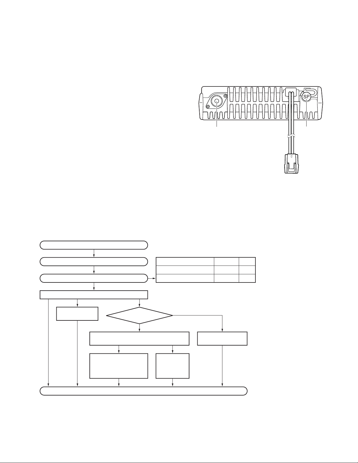
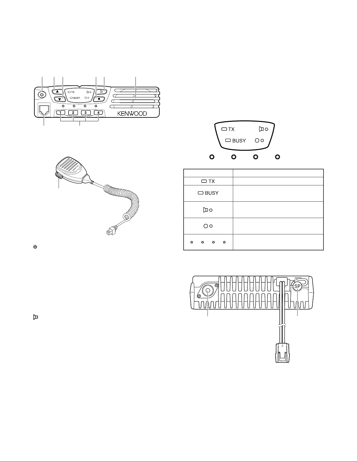
NOTE
If you do not intend to use the 3.5-mm jack for the external
speaker, fit the supplied speaker-jack cap to stop dust and
sand from getting in.
Antenna
connector
Power input
connector
Speaker
jack cap
SYSTEM SET-UP
Merchandise received
License and frequency allocated by FCC
Choose the type of transceiver
Transceiver programming
KES-3
External speaker
(Option)
Modem GPS receiver or
Modem GPS controller
KCT-39
Connection cable
KCT-36
Extension cable
KGP-2A
KGP-2B
Frequency range (MHz) RF power
146~174 50W K,M
136~162 50W K2,M2
See page 8.
A personal computer (IBM PC or compatible), programming interface (KPG-46),
and programming software (KPG-70D) are required for programming.
(Option)
KCT-18
Ignition sense cable
Delivery
or
Mobile data
(Option)
KDS-100
terminal
(Option)(Option)
(Option)
Type
3
TK-7102H
OPERATING FEATURES
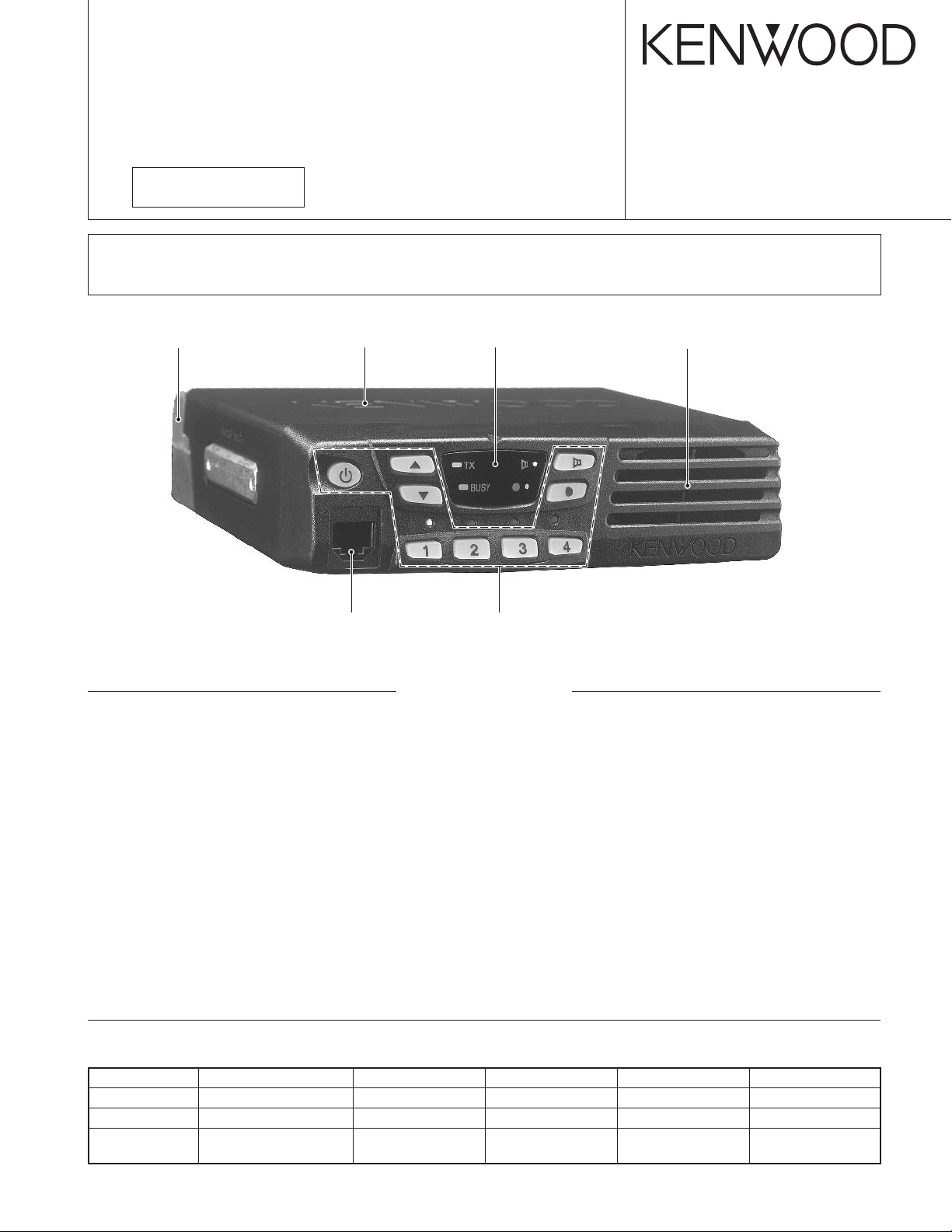
1. Controls and Functions
1-1. Front Panel
q
we tr
u
y
1-2. Microphone
o
q (Power) switch
Press to switch the transceiver ON. Press and hold for
approximately 1 seconds to switch the transceiver OFF.
w ▲ key
Press to increase the volume level.
e ▼ key
Press to decrease the volume level.
r ● key
PF (Programmable Function) key. The default setting of
this key is None (no function). The programmable functions available for this key are listed below.
key
t
PF (Programmable Function) key. The default setting of
this key is Monitor. Other programmable functions available for this key are listed below.
y 1/ 2/ 3/ 4 keys
Press to select a channel from 1 to 4.
u Microphone jack
Insert the microphone plug into this jack (the microphone
is an optional accessory).
i Speaker
Internal speaker.
o PTT switch
Press this switch, then speak into the microphone to call a
station.
i
1-3. Auxiliary Programmable Functions
• Emergency • Scan On/OFF
• Key Lock • Talk Around
• Monitor • Temporary Delete
• None (no function) • AUX
• Horn Alert • Scan + Temporary Delete
1-4. Display
Indicator Description
Light while transmitting.
Lights when a signal is detected on
the currently selected channel.
Lights while the function programmed
onto its corresponding key is activated.
Lights while the function programmed
onto its corresponding key is activated.
Lights to display the currently selected
channel (1~ 4).
1-5. Rear panel
Antenna
connector
Power input
connector
External
speaker
jack
4

OPERATING FEATURES
TK-7102H
2. Operation Features
The TK-7102H is a VHF FM radio designed to operate in
conventional format. The programmable features are summarized.
3. Transceiver Controls and Indicators
3-1. Front Panel Controls
All the keys on the front panel are momentary-type push
buttons. The functions of these keys are explained below.
• POWER key
Transceiver POWER key. When the power is switched
off, all the parameters are stored in memory. When the
power is switched on again, the transceiver returns to the
previous conditions.
• CHANNEL keys
• MONITOR key (Programmable)
• ● key (Programmable)
• VOLUME UP/DOWN key
When the key is pressed, the volume level is increased/
decreased and repeats if held for 200ms or longer.
• BUSY/TX LED
The BUSY indicator (Green LED) shows that the channel is
in use. The TX indicator (Red LED) shows that you are transmitting.
3-2. Programmable Keys
The FPU (KPG-70D) enables programmable keys to select
the following functions.
• Emergency
• Key Lock
• Monitor
• Scan ON/OFF
• Talk Around
• Temporary Delete
• None
• AUX
• Horn Alert
• Scan + Temporary Delete
• Emergency
Pressing this key for longer than 1 second causes the
transceiver to enter the emergency mode. The transceiver
jumps to the programmed “Emergency channel” and transmits for 25* seconds.
The transceiver disables mic mute while transmitting. After finishing transmission, the transceiver receivers for 5*
seconds. The transceiver Mute* the speaker while receiving.
Following the above sequence, the transceiver continues to
transmit and receive.
* Default value.
• Key lock
Pressing this key causes the transceiver to accept entry of
only the [Vol Up/Down]*, [Key lock], Microphone [PTT],
[Monitor], [Emergency], and [Power] keys.
* Programmable
• Monitor
Used to release signalling (press once) or squelch (press
and hold for approximately two seconds) when operating as a
conventional. It is also used to reset option signalling.
• Scan ON/OFF
Press this key starts scanning. Pressing this key stops
scanning.
• Talk around
Press this key, the transceiver uses the receive frequency
and the tone for transmission.
The operator can call the other party directly (without repeater). Press this key again, the talk around function goes
off.
• Temporary delete
The “Add” channel contained in the scan sequence, and
“Delete” channel is not contained. In the scan mode, this
key switches the channel delete temporarily (Press and hold
for approximately one second).
When the transceiver is turned off, the transceiver exits
the scan or switches the scan function off.
• None
Sounds error operation beep, and no action will occur.
Use this function when the transceiver is required to be more
simple operated.
• AUX
Press to activate the auxiliary port. Press again to deactivate the auxiliary port. Auxiliary is used with optional boards,
allowing you to activate and deactivate these optional functions. While activated, the AUX icon appears on the display.
• Horn alert
Horn Alert is a useful feature that will notify you of a received call while you are away from your vehicle. The transceiver is programmed to sound the vehicle horn or some
other external alert device (such as the vehicle headlights)
when a call is received that has correct signalling.
• Scan + Temporarily delete
To temporarily remove a channel from the Scan list, press
and hold this key for approximately one second during Scan,
while Scan is paused on the undesired channel, to temporarily remove that channel from the scanning sequence. After switching the Scan function OFF, or switching the transceiver OFF and then ON again, the Scan settings return to
normal.
5

TK-7102H
OPERATING FEATURES
4. Scan Operating
■ SCAN start condition
Two or more channels must be added to all channels that
can be scanned. The transceiver must be in normal receive
mode (PTT off).
When you activate the key programmed to the scan ON/
OFF function, the scan starts. The indicator next to the programmed key LED blinks.
■ Scan stop condition
The scan stops temporarily if the following conditions are
satisfied.
1) A carrier is detected, then QT/DQT matches on channels
for which receive the QT/DQT is set by the programming
software.
2) A carrier is detected on the channels for which receiving
QT/DQT is not set by the programming software or when
the monitor (signalling cancel) function is activated.
■ Revert channel
The revert channel is used to transmit during scanning and
set by the programming software (KPG-70D).
1) Selected channel
The transceiver reverts to the channel before scanning or
the channel that you changed during scan.
2) Selected with talkback
The transceiver reverts to the selected channel prior to
scan initiation.
However, if a call is received on a channel other then the
selected channel and PTT is pressed before scanning re-
sume, the transceiver “talks back” on the current receive
channel.
■ Scan end
When you press the key programmed to the scan function
during scan mode, the scan ends.
The indicator next to the programmed key LED turns off.
■ Temporary delete
It is possible to delete channel temporary during scan.
When scan stops on unnecessary channel for example by interference of the other party, activate the delete function (for
example press and hold the key for approximately one second), then that channel is deleted temporarily and scan restart immediately.
The temporary deleted channels return to pre-set delete/
add channels, when the transceiver is turned off or the scan
function is switched off.
5. Details of Features
■ Time-out timer
The time-out timer can be programmed in 30 seconds increments from 30 seconds to five minutes and off. If the
transmitter is transmitted continuously for longer than the
programmed time, the transmitter is disabled and a warning
tone sounds while the PTT button is held down. The warning
tone stops when the PTT button is released.
■ PTT ID
PTT ID provides a DTMF ANI or MSK ID to be sent with
every time PTT (connect ID at beginning of transmission, disconnect ID at end of transmission, or both).
You can program PTT ID “on” or “off” for each group
channel (DTMF). The contents of ID are programmed for
each transceiver.
The transceiver is capable to have ID. The format is
DTMF. The timing that the transceiver sends ID is programmable.
BOT : Connect ID is sent on beginning of transmission.
EOT : Disconnect ID is sent on end of transmission.
Both : Connect ID is sent on beginning of transmission
and disconnect ID is sent on end of transmission.
There is also “PTT ID” setting for each channel.
■ Off hook decode
If the Off hook decode function has been enabled, removing and replacing the microphone on the hook has no effect
for decoding QT/DQT and option signalling.
■ “TOT” pre-alert
The transceiver has “TOT” pre-alert timer. This parameter selects the time at which the transceiver generates
“TOT” pre-alert tone before “TOT” is expired.
“TOT” will be expired when the selected time passes
from a TOT pre-alert tone.
■ “TOT” re-key time
The transceiver has “TOT” re-key timer. This timer is the
time you can not transmit after “TOT” exceeded. After
“TOT” re-key time expired you can transmit again.
■ “TOT” reset time
The transceiver has “TOT” reset timer. This timer is the
minimum wait time allowed during a transmission that will
reset the “TOT” count.
“TOT” reset time causes the “TOT” to continue even after PTT is released unless the “TOT” reset timer has expired.
■ Clear to transpond
The transceiver waits the transpond of DTMF if channel is
busy until channel open. This feature prevents the interference to other party.
6. Option Signalling (DTMF)
Built-in DTMF decoder is available for option signalling.
It is possible to use individual call, group call, Stun.
If the option signalling matches, a predetermined action
will occur.
If option signalling matches on a channel is set up with
option signalling, the channel LED will flash and option signalling will be released. The transpond or alert tone will sound.
While option signalling matches (or if option signalling is
deactivated when you are transmitting), you can mute or
unmute QT/DQT/Carrier.
6

OPERATING FEATURES
TK-7102H
■ SP Unmute
You can select the type of SP Unmute system for each
channel. The selection is as follows.
Carrier, QT/DQT:
Channel with this option will not check ID Code in order to
open its speaker.
Carrier+DTMF, QT/DQT+DTMF:
Channel that is set with this option will have to check for
ID Code in order to open its speaker.
Default:
Carrier, QT/DQT.
SP unmute
Carrier None None Carrier Sounds
Carrier+DTMF
QT/DQT Yes None Carrier Not Sounds
QT/DQT+DTMF
Channel setting
QT/DQT
DTMF condition
Yes Carrier Sounds
None Yes Carrier Not Sounds
Yes Carrier Not Sounds
Yes Yes Carrier Not Sounds
RX condition Speaker
Carrier+DTMF Sounds
Carrier+DTMF Sounds
Carrier+QT/DQT Sounds
Carrier+QT/DQT Sounds
Carrier+QT/DQT+DTMF
Carrier+DTMF Not Sounds
Carrier+QT/DQT Not Sounds
Carrier+QT/DQT+DTMF
Carrier+DTMF Not Sounds
Sounds
Sounds
7. Audible User Feedback Tones
The transceiver outputs various combinations of tones to
notify the user of the transceiver operating state.
Refer to the help file on the KPG-70D, regarding the func-
tions that are not listed below.
■ Stun on tone
When a stun code is received, transpond tone sounds.
■ Stun off tone
When a stun release code is received, transpond tone
sounds.
■ Group call tone
Sounds when a group call with the correct DTMF option
signalling is received, repeats 7 times. You can select yes or
no in the Alert tone level setting.
■ Individual call tone
Sounds when an individual call with the correct DTMF option signalling is received. You can select yes or no in the
Alert tone level setting.
■ Key input error tone
Sounds when a key is pressed but that key cannot be
used. You can select yes or no for the optional feature's
warning tone.
■ Transpond tone
Sounds when an individual call with the correct DTMF option signalling is received. For group calls, only the group
tone will sound, not the transpond tone.
Note :
When QT/DQT is not used, QT/DQT and QT/DQT+DTMF
can not be selected.
When DTMF is not used, Carrier+DTMF and QT/
DQT+DTMF can not be selected.
■ Auto Reset
If option signalling matches a group set up with option signalling, option signalling is released. After matching option
signalling, option signalling will temporarily reset automatically.
■ Stun
If the stun code matches, a predetermined action will occur. Whether option signalling is activated or not, when stun
matches on any channel, the transceiver will become TX inhibited or TX/RX inhibited. While stun is active, if the stun
code + “#” code is received, stun will deactivate.
When stun matches, transpond will function. Alert will
not be output.
■ Pre alert tone
Sounds prior to the TOT TX inhibit activation. If TOT pre
alert is set, the tone sounds at the amount of time programmed, before the TOT expires (TOT time – TOT pre alert
time = Pre alert tone sounding time). You can select yes or
no for the optional feature’s warning tone.
■ Transmit protection
The final FET is protected against heat while transmitting
by making the radio cuts down TX power when the temperature of the final FET becomes higher than reference. After
that, if the temperature continue to rise, transmission is
stopped. The final FET is also protected against over voltage
by having the radio to check that the voltage of power supply
connected to the radio is not higher than about 17V when the
radio is turned on, otherwise it can not transmit. In both
cases when transmission is stopped, a beep will continue to
sound until the PTT key is released.
7
TK-7102H
REALIGNMENT
1. Modes
User mode
PC mode
Clone mode
Mode Function
User mode For normal use.
PC mode Used for communication between the
Data programming Used to read and write frequency data
mode and other features to and from the radio.
PC test mode Used to check the radio using the PC.
PC tuning mode Used to tune the radio using the PC.
Clone mode Used to transfer programming data from
Data programming mode
PC test mode
radio and PC (IBM compatible).
This feature is included in the FPU.
one radio to another.
PC tuning mode
2. How to Enter Each Mode
Mode Operation
User mode Power ON
PC mode Received commands from PC
Clone mode [1]+Power ON (Two seconds)
3-2. Connection Procedure
1. Connect the TK-7102H to the personal computer with the
interface cable.
2. When the Power is switched on, user mode can be entered immediately. When the PC sends a command, the
radio enters PC mode.
When data is transmitted from transceiver, the red LED
blink.
When data is received by the transceiver, the green LED
blink.
In the PC mode, 4CH LEDs, [MON] LED and [●] LED are
turned on.
Notes :
• The data stored in the personal computer must match
model type when it is written into the EEPROM.
• Attach the interface cable, then change the TK-7102H to
PC mode.
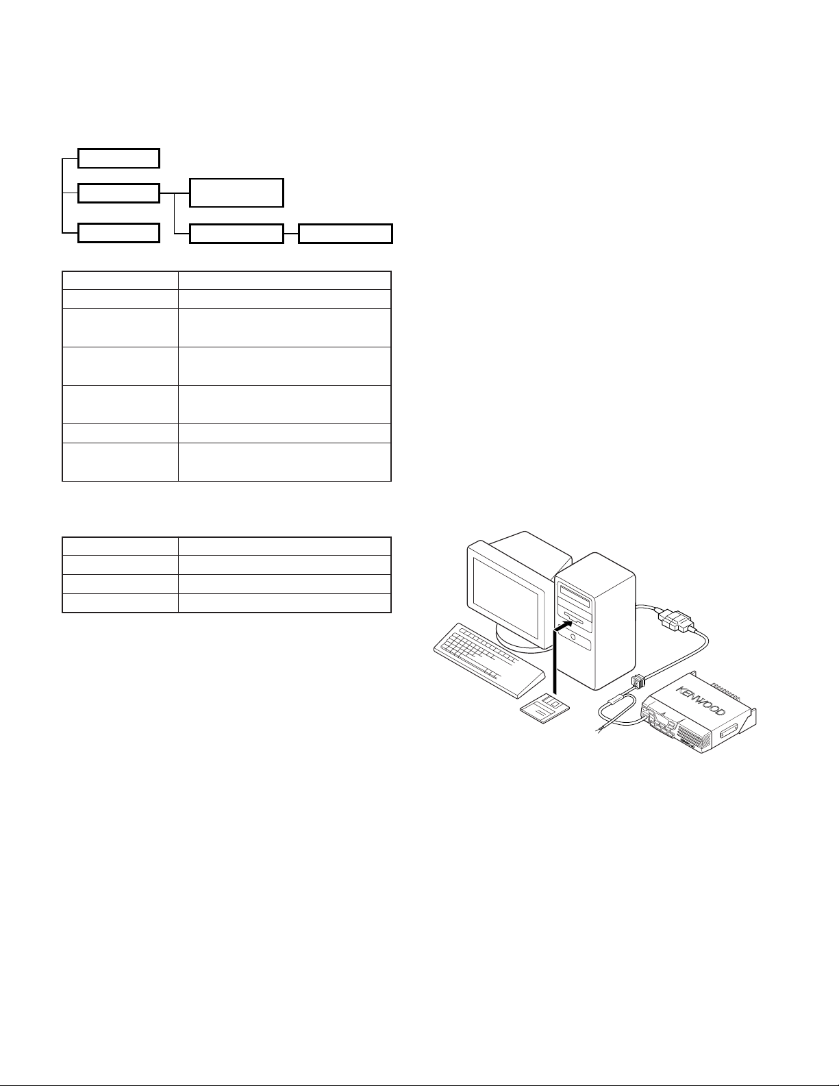
3-3. KPG-46 Description
(PC programming interface cable : Option)
The KPG-46 is required to interface the TK-7102H to the
computer. It has a circuit in its D-subconnector (25-pin) case
that converts the RS-232C logic level to the TTL level.
The KPG-46 connects the modular microphone jack of the
TK-7102H to the computers RS-232C serial port.
IMC-PC
KPG-46
3. PC Mode
3-1. Preface
The TK-7102H transceiver is programmed using a personal computer, a programming interface (KPG-46) and programming software (KPG-70D).
The programming software can be used with an IBM PC
or compatible. Figure 1 shows the setup of an IBM PC for
programming.
8
KPG-70D
TK-7102H
Fig. 1
3-4. Programming Software Description
The KPG-70D programming disk is supplied in 3-1/2" disk
format. The software on this disk allows a user to program
TK-7102H radio via a programming interface cable (KPG-46).
3-5. Programming With IBM PC
If data is transferred to the transceiver from an IBM PC
with the KPG-70D, the destination data (basic radio information) for each set can be modified.
REALIGNMENT
TK-7102H
4. Clone Mode
Programming data can be transferred from one radio to
another by connecting them via their modular microphone
jacks. The operation is as follows (the transmit radio is the
master and the receive radio is the slave).
Note :
Clone mode should enabled.
1. Turn the master TK-7102H power ON with the [1] key held
down. The TK-7102H [●] LED is turned on.
2. Power on the slave TK-7102H.
3. Connect the cloning cable (No. E30-3382-05) to the modu-
lar microphone jacks on the master and slave.
4. Press the [●] key on the master TK-7102H transceiver.
The data of the master is sent to the slave. While the mas-
ter is sending data, [TX] LED blinked. While the slave is
receiving the data, 4 LEDs, [MON] LED, [●] LED are
turned on and [BUSY] LED blinked. When cloning of data
is completed, the master [TX] LED turned off, and the
slave automatically operates in the User mode. The slave
can then be operated by the same program as the master.
5. The other slave can be continuously cloned. Carry out the
operation in step 2 to 4.
4-1. Adding the data password.
If the data password is set in the optional feature menu,
you must enter the password (Master transceiver) to activate
a clone mode.
you can use 1, 2, 3, and 4 to configure the password. The
maximum length of the password is 10 digits.
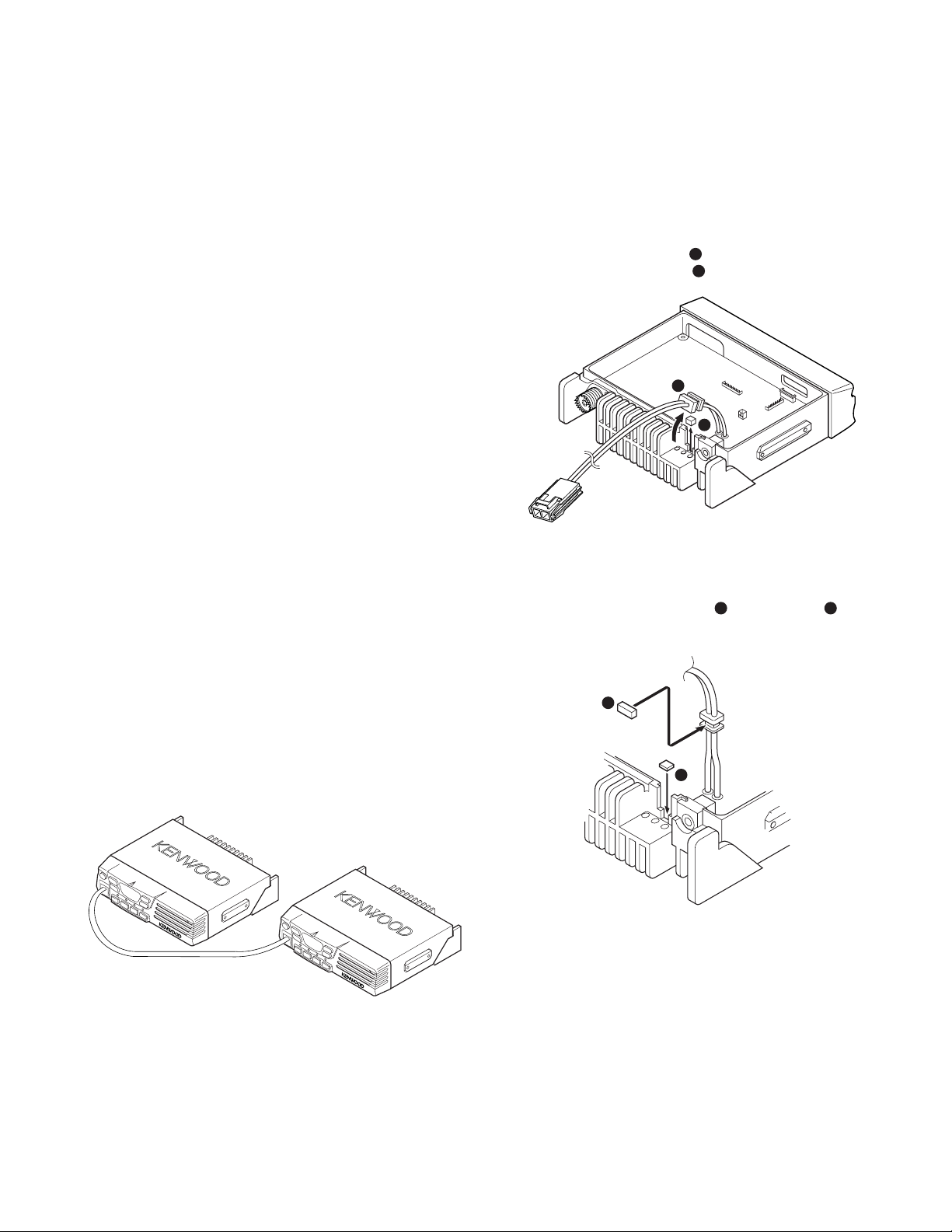
5. Accessory Connection Cable (KCT-39)
The KCT-39 is an accessory connection cable for connecting external equipment. The connector has 15 pins and the
necessary signal lines are selected for use.
5-1. Installing the KCT-39 in the Transceiver
1. Lift the DC cord bushing (1) from the chassis. Peel the
pad as shown in Figure 3 (
2. Stick the pad to the DC cord (3) and chassis (4), both
of which are supplied with the KCT-39.
2
1
2
Fig. 3
).
1. [1]+Power ON.
2. [1]~[4] LED, and MON LED are turned ON.
3. Enter the password using [1]~[4] keys.
4. Press [MON] key.
5. If the password matches, the transceiver enters a clone
mode. Otherwise, transceiver beeps and returns to the
password input mode.
Clone cable
(E30-3382-05)
Fig. 2
3
4
Fig. 4
9
TK-7102H
REALIGNMENT
3. Insert the KCT-39 cable (5) into the chassis (6). The
7
wire harness band (
) must be inside the chassis and
face down.
4. Connect the KCT-39 to the TX-RX unit as shown in Figure
8
).
5 (
Avoid forming the wiring towards
the shielding cover closure area.
CN2
Chassis
Cushion
Chassis
Face down
End view of this area
5
7
Wire harness
band (Stopper)
KCT-39
sumi tube
PCB
6
CN3
B
8
A
■ Accessory Port Function
No. Color Internal Name
1471013
2581114
3691215
1 Red CN2-1 SB
2 Pink CN3-1 IGN
3 Black CN2-3 GND
4 Brown CN3-3 DETO
5 Orange CN3-2 DATAI
6 Yellow CN2-8 FNC4
7 Green CN2-7 FNC3
8 Blue CN2-9 FNC5
9 Purple CN2-12 FNC8
10 Gray CN2-10 FNC6
11 White CN2-11 FNC7
12 NC NC
13 NC NC
14
Sky blue
15
Turquoise
connector
CN2-6 FNC2
CN2-5 FNC1
6. Ignition Sense Cable (KCT-18)
The KCT-18 is an optional cable for enabling the ignition
function. The ignition function lets you turn the power to the
transceiver on and off with the car ignition key.
Fig. 5
5. Connect the KCT-39 to the external accessory by inserting
the crimp terminal (
which are supplied with the KCT-39.
13
15
1
10
3
9
9
) into the square plug (10), both of
6-2. Connecting the KCT-18 to the Transceiver
1. Install the KCT-39 in the transceiver. (See the KCT-39 section)
1
2. Insert the KCT-18 lead terminal (
2
39 (
).
13
1
15
3
1
2
) into pin 2 of the KCT-
Fig. 7
10
Fig. 6
REALIGNMENT / INSTALLATION
TK-7102H
6-3. Modifying the Transceiver
Modify the transceiver as follows to turn the power on and
off with the ignition key.
1. Remove the jumper resistor (0Ω) R71 of the TX-RX unit.
■ Setting With the KPG-70D
Select “External Devices” from the “Edit” menu and en-
able the “Ignition Sense”.
TX-RX UNIT
Component side
CN2
R71
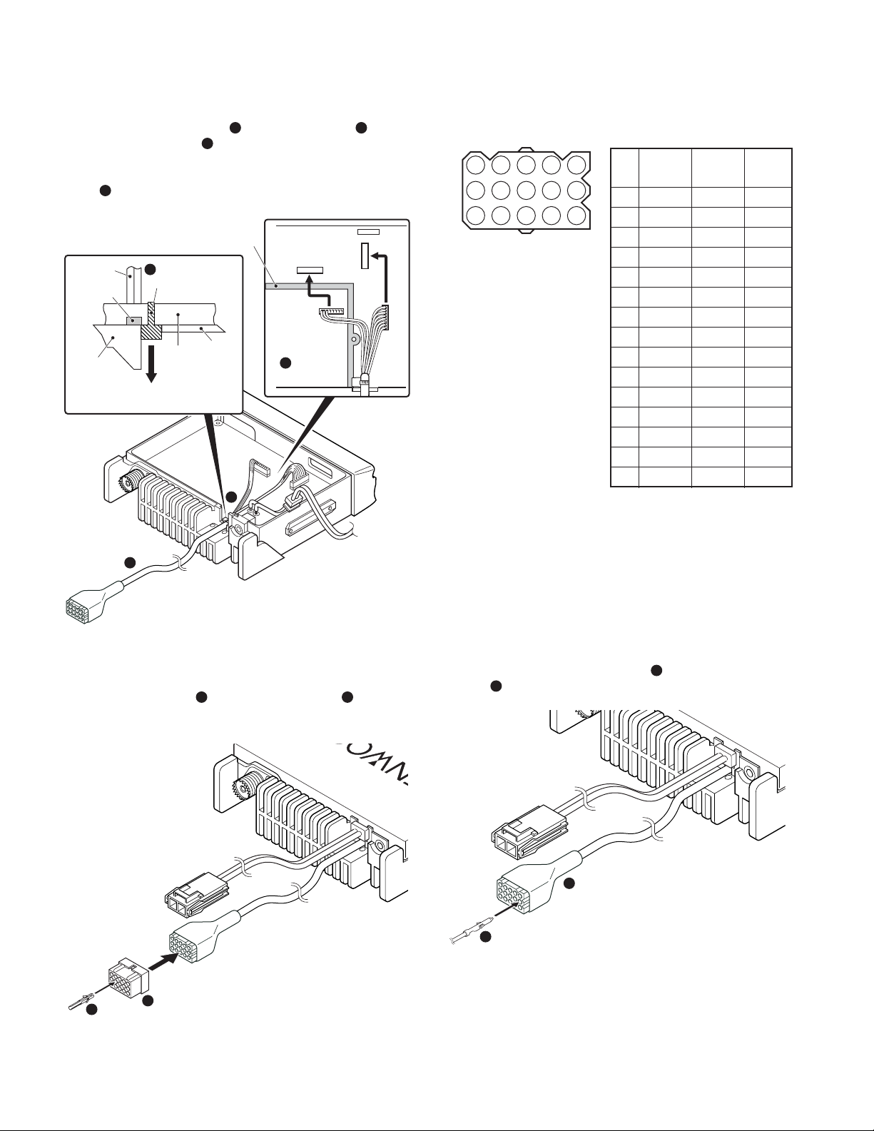
INSTALLATION
1. Optional Board
1-1. Voice Scrambler Board Connection
■ Modification
1. Remove the cabinet and shielding cover from the transceiver.
2. Delete R202 and R267 on the TX-RX unit.
TX-RX UNIT
Component side
CN3
R267
R202
Fig. 8
Fig. 1
■ Connection
The functions of pins of CN2 and CN3 on the TX-RX unit
are shown in the TERMINAL FUNCTION section (page 34).
12 pins lead wire
with connector (A)
CN2
1
12
CN3
1
E37-1081-05
1
3
7
8
9
10
11
12
11 pins lead wire
with connector (B)
E37-1080-05
1
4
5
7
9
8
7
D
C
B
A
12
5
6
A12
Voice scrambler
board
A
BA11
CA10
DA9
E
1
2
3
4
5B5
6B7
7A8
8A7
9A3
10B11
11B9
12B4
E18
9
11
11
11
10
Fig. 2
11
TK-7102H
INSTALLATION
■ Pins Connection
Voice scrambler
functions with connector (A) with connector (B)
A A-12 –
B A-11 –
C A-10 –
D A-9 –
5– B-5
6– B-7
7 A-8 –
8 A-7 –
9 A-3 –
10 – B-11
11 – B-9
12 – B-4
Avoid forming the wiring towards shielding cover closure area.
TX-RX UNIT
Component side
12 pins lead wire 11 pins lead wire
1-2. Example for Connection
■ Picture (Trunking Board)
Insulation sheet
Cushion C
Trunking board
Cushion D
(G13-1972-04)
Cushion B
CN2
to CN2 and CN3
Front side
CN3
Voice scrambler
board
to CN2
and CN3
Cushion (G13-1963-04)
Voice scrambler board
Cushion (G13-1964-04)
Fig. 3
■ Setting With the KPG-70D
Select “External Devices” from the “Edit” menu and set
the “Scrambler”.
Note :
The voice scrambler board is connected subsequent to the
de-emphasis circuit.
TX-RX unit
CN4
Front side
Fig. 4
■ Setting With the KPG-70D
Select “External Devices” from the “Edit” menu and set
the “SmarTrunk”.
12
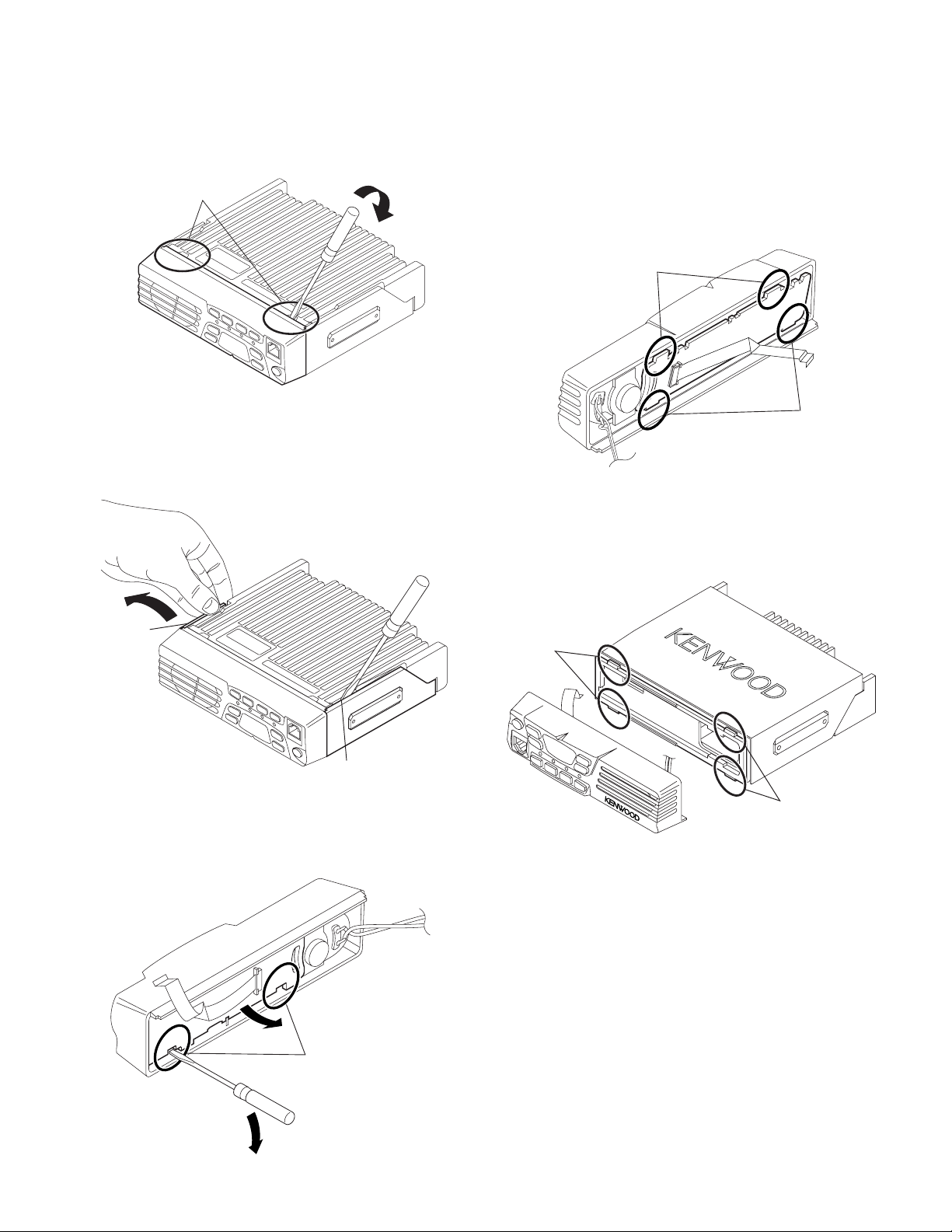
DISASSEMBLY FOR REPAIR
TK-7102H
1. When you remove the panel, turn the transceiver up side
down. Detach the panel by lifting the tabs as shown below.
Tabs
Fig. 1
2. To remove the cabinet, first turn the transceiver up side
down. Detach the cabinet by prying the tabs as shown
below.
4. Mount the display unit
To mount the display unit on the panel, follow the correct
procedures shown to ensure easy display unit assembly
and good fitting onto the panel.
q Snap in bottom of display unit first.
w Snap in top of displaly unit.
w
q
Fig. 4
5. When mounting the front panel, match the 4 tabs of the
chassis with the panel, being sure they attach securely.
Tabs
Tabs
Fig. 2
3. To remove the display unit PCB, detach the PCB by lifting
at the indents of the PCB as shown below.
Indents
Tabs
Tabs
Fig. 5
Fig. 3
13

TK-7102H
CIRCUIT DESCRIPTION
Frequency Configuration
The receiver utilizes double conversion. The first IF is
49.95MHz and the second IF is 450kHz. The first local oscillator signal is supplied from the PLL circuit.
The PLL circuit in the transmitter generates the necessary
frequencies. Figure 1 shows the frequencies.
ANT
ANTSWRF
POWER
AMP
AMP
RF
AMP
1st
MIX
MCF
49.95MHz
RX
TX
1/2
CF 450kHz
IF SYSTEM
50.4MHz
X3
multiply
TCXO
PLL/VCO
AF
PA
16.8MHz
MIC
AMP
SP
MIC
Fig. 1 Frequency configuration
Receiver System
The receiver is double conversion superheterodyne. The
frequency configuration is shown in Figure 1.
■ Front-end RF Amplifier
An incoming signal from the antenna is applied to an RF
amplifier (Q353) after passing through a transmit/receive
switch circuit (D603, D604, D605 are off) and a band pass
filter (L357, L356 and varactor diodes : D353, D354). After
the signal is amplified (Q353), the signal is filtered through a
band pass filter (L354, L355 and varactor diodes: D351,
D352) to eliminate unwanted signals before it is passed to
the first mixer.
The voltage of these diodes are controlled by tracking the
CPU (IC101) center frequency of the band pass filter. (See
Fig. 2)
■ First Mixer
The signal from the RF amplifier is heterodyned with the
first local oscillator signal from the PLL frequency synthesizer
circuit at the first mixer (Q352) to create a 49.95MHz first
intermediate frequency (1st IF) signal. The first IF signal is
then fed through one pair of monolithic crystal filter (MCF :
XF351) to further remove spurious signals.
■ IF Amplifier
The first IF signal is amplified by Q351, and the enters
IC301 (FM processing IC). The signal is heterodyned again
with a second local oscillator signal within IC301 to create a
450kHz second IF signal. The second IF signal is then fed
through a 450kHz ceramic filter (Wide : CF301, Narrow :
CF302) to further eliminate unwanted signals before it is amplified and FM detected in IC301.
Item Rating
Nominal center frequency 49.95MHz
Pass bandwidth ± 5.0kHz or more at 3dB
35dB stop bandwidth ±20.0kHz or less
Ripple 1.0dB or less
Insertion loss 5.0dB or less
Guaranteed attenMuation 80dB or more at fo± 1MHz
Spurious : 40dB or more within fo±1MHz
Terminal impedance 350Ω / 5.5pF
Table 1 Crystal filter (L71-0591-05) : XF351
Item Rating
Nominal center frequency 450kHz
6dB bandwidth ±6.0kHz or more
50dB bandwidth ±12.5kHz or less
Ripple 2.0dB or less
Insertion loss 6.0dB or less
Guaranteed attenuation 35.0dB or more within fo± 100kHz
Terminal impedance 2.0kΩ
Table 2 Ceramic filter (L72-0993-05) : CF301
Item Rating
Nominal center frequency 450kHz
6dB bandwidth ±4.5kHz or more
50dB bandwidth ±10.0kHz or less
Ripple 2.0dB or less
Insertion loss 6.0dB or less
Guaranteed attenuation 60.0dB or more within fo± 100kHz
Terminal impedance 2.0kΩ
Table 3 Ceramic filter (L72-0999-05) : CF302
CF301 (Wide)
14
ANT
D602~605
ANT
SW
IC161
D/A
L357,356
D353,354
BPF
TV
CPU
Q353
RF AMP
L354,355
D351,352
Q352
BPF
MIX
IC402
1/2 divider
1st local
OSC (VCO/PLL)
XF351
MCF
Fig. 2 Receiver system
Q351
IF AMP
X401
TCXO
CF302 (Narrow)
IC301
IF system
Q302
X3 multiply
IC161
D/A CONVERTER
W/NO
(EVOL2)

Q301
NOISE AMP
D301IC301 IC101
AFO
RSSI
DET
CPU
IF
SYSTEM
SQIN
RSSI
CIRCUIT DESCRIPTION
TK-7102H
■ Wide/Narrow Changeover Circuit
The Wide port (pin 65) and Narrow port (pin 64) of the CPU
is used to switch between ceramic filters. When the Wide
port is high, the ceramic filter SW diodes (D303, D302) cause
CF301 to turn on to receive a Wide signal.
When the Narrow port is high, the ceramic filter SW diodes (D303, D302) cause CF302 to turn on to receive a Narrow signal.
IC301
R319
IF System
R318
R317
Wide
IC6 65pin
Narrow
IC101 64pin
IF_IN MIX_O
CF301
(Wide)
CF302
D303 D302
(Narrow)
R320
Fig. 3 Wide/Narrow changeover circuit
■ AF Signal System
The detection signal from IF IC (IC301) goes to D/A converter (IC161) to adjust the gain and is output to AF filter
(IC251) for characterizing the signal. The AF signal output
from IC251 and the DTMF signal, BEEP signal are summed
and the resulting signal goes to the D/A converter (IC161).
The AFO output level is adjusted by the D/A converter. The
signal output from the D/A converter is input to the audio
power amplifier (IC252). The AF signal from IC252 switches
between the internal speaker and speaker jack (J1) output.
IC301
IF IC
IC161 IC251
D/A
CONV.
W/NO
(EVOL2)
AF
Filter
IC161
D/A
CONV.
IC252 SP
AF PA
Fig. 4 AF signal system
■ Squelch Circuit
The detection output from the FM IF IC (IC301) passes
through a noise amplifier (Q301) to detect noise. A voltage is
applied to the CPU (IC101). The CPU controls squelch according to the voltage (SQIN) level. The signal from the RSSI
pin of IC301 is monitored. The electric field strength of the
receive signal can be known before the SQIN voltage is input
to the CPU, and the scan stop speed is improved.
Fig. 5 Squelch circuit
PLL Frequency Synthesizer
The PLL circuit generates the first local oscillator signal for
reception and the RF signal for transmission.
■ PLL
The frequency step of the PLL circuit is 5 or 6.25kHz. A
16.8MHz reference oscillator signal is divided at IC401 by a
fixed counter to produce the 5 or 6.25kHz reference frequency. The voltage controlled oscillator (VCO) output signal
is buffer amplified by Q410, then divided in IC401 by a dualmodule programmable counter. The divided signal is compared in phase with the 5 or 6.25kHz reference signal in the
phase comparator in IC401. The output signal from the
phase comparator is filtered through a low-pass filter and
passed to the VCO to control the oscillator frequency. (See
Fig. 6)
■ VCO
The operating frequency is generated by Q406 in transmit
mode and Q405 in receive mode. The oscillator frequency is
controlled by applying the VCO control voltage, obtained
from the phase comparator, to the varactor diodes (D405 and
D406 in transmit mode and D403 and D404 in receive mode).
The TX/RX pin is set low in receive mode causing Q408 and
Q407 to turn Q406 off, and turn Q405 on. The TX/RX pin is
set high in transmit mode. The outputs from Q405 and Q406
are amplified by Q410 and sent to the RF amplifiers.
PLL
DATA
16.8MHz
IC401 : PLL IC
5kHz/6.25kHz
1/N
1/M
comparator
5kHz/6.25kHz
REF
OSC
Phase
LPF
Charge
pump
Fig. 6 PLL circuit
D405,406
D403,404
Q406
TX VCO
Q405
RX VCO
Q404
AMP
Q410
BUFF
AMP
Q407,408
T/R SW
15

TK-7102H
CIRCUIT DESCRIPTION
■ Unlock Circuit
During reception, the 8RC signal goes high, the 8TC signal
goes low, and Q34 turns on. Q33 turns on and a voltage is
applied to the collector (8R). During transmission, the 8RC
signal goes low, the 8TC signal goes high and Q36 turns on.
Q35 turns on and a voltage is applied to 8T.
The CPU in the control unit monitors the PLL (IC401) LD
signal directly. When the PLL is unlocked during transmission, the PLL LD signal goes low. The CPU detects this signal and makes the 8TC signal low. When the 8TC signal goes
low, no voltage is applied to 8T, and no signal is transmitted.
8C
8R 8T
Q33
SW
Q34
SW
8RC
IC101
CPU
Q35
SW
Q36
SW
LD
8TC
IC401
PLL
PLL lock
: LD “H”
Fig. 7 Unlock circuit
Transmitter System
■ Outline
The transmitter circuit produces and amplifies the desired
frequency directly. It FM-modulates the carrier signal by
means of a varicap diode.
■ Power Amplifier Circuit
The transmit output signal from the VCO passes through
the transmission/reception selection diode (D409) and amplified by Q501, Q502 and Q503. The amplified signal goes to
the final amplifier (Q504) through a low-pass filter. The lowpass filter removes unwanted high-frequency harmonic components, and the resulting signal is goes the antenna terminal.
■ APC Circuit
The automatic transmission power control (APC) circuit
detects part of a final amplifier output with a diode (D606,
D607) and applies a voltage to IC501. IC501 compares the
APC control voltage (PC) generated by the D/A converter
(IC161) and DC amplifier (IC203) with the detection output
voltage. IC501 generates the voltage to control Q503 and
Q504 and stabilizes transmission output.
The APC circuit is configured to protect over current of
Q503 and Q504 due to fluctuations of the load at the antenna
end and to stabilize transmission output at voltage and temperature variations.
MIC/IDC
NJM2100V
MIC KEY
INPUT
IC161 Q406
D/A
CONVERTER
M62363FP
X401
TCXO
16.8MHz
IC202IC201MIC
Splatter
FILTER
NJM2904V
IC101
CPU
30622MAA
-B83GP
VCO
2SK508NV
(K52)
IC401
PLL
MB15A02
BUFFER
2SC5108
2SC4649
D409
PC
IC161
3pin
IC203
SUM AMP
NJM2902V
IC161
CONVERTER
M62363FP
Q410
(Y)
Q404
RF AMP
(N,P)
D/A
Q501
RF
AMP
IC203
DC
AMP
IC161
D/A
CONVERTER
M62363FP
IC402
1/2
DIVIDER
UPB1509GV
BUFFER
NJM2902V
Q411
RF AMP
2SC4649
(N,P)
IC203
Q501
RF AMP
2SC3357
Fig. 8 Transmitter system
Q502
PRE
DRIVE
AMP
Q503
DRIVE
AMP
IC501
Q504
FINAL
AMP
APC
CONTROL
DRIVE AMP
D602~D605
ANT
SW
D606
D607
VR1
Q502
PRE
2SC3357
LPF
POWER
DET
Q503
DRIVE AMP
PD55003TR
ANT
ANT
Q504
FINAL AMP
RD70HVF1
-01
16
Fig. 9 APC circuit

CIRCUIT DESCRIPTION
TK-7102H
Control Circuit
The CPU carries out the following tasks:
1) Controls the WIDE, NARROW, TX/RX outputs.
2) Adjusts the AF signal level of the AF filter (IC251) and
turns the filter select compounder on or off.
3) Controls the display unit.
4) Controls the PLL (IC401).
5) Controls the D/A converter (IC161) and adjusts the volume, modulation and transmission power.
CK
DT
IC101
CPU
LD
PLLE
Fig. 10 Control circuit
■ Memory Circuit
The transceiver has an 64k-bit EEPROM (IC66). The
EEPROM contains adjustment data. The CPU (IC101) controls the EEPROM through three serial data lines.
EEPCK
IC101
CPU
EEPDT
EEPWP
Fig. 11 Memory circuit
■ Display Circuit
The shift register controls the display LEDs through the CL
and DI lines from the CPU (IC101).
When the transceiver is busy, LED G line becomes high
impedance, turning on Q4 and the green LED (D11) lights, in
transmit mode, the LED R line becomes low impedance, and
the red LED (D12) lights.
Backlit LEDs (D1~D4) are provided and will only goes off
when MBL line becomes low impedance.
When a function key (MON, PF, C1, C2, C3 or C4) is se-
lected, its respective line becomes low impedance (LED
MON, LED PF, LED C1, LED C2, LED C3 or LED C4), the
amber LED lights.
IC161
D/A
converter
IC401
PLL
IC66
EEPROM
■ Key Matrix Circuit
The TK-7102H front panel has function keys. Each of
them is connected to a cross point of a matrix of the KMI1 to
KMO2 ports of the microprocessor. The KMO1 to KMO2
ports are always high, while the KMI1 to KMI4 ports are always low.
The microprocessor monitors the status of the KMI1 to
KMO2 ports. If the state of one of the ports changes, the
microprocessor assumes that the key at the matrix point corresponding to that port has been pressed.
1
2
3P
4
IC101
CPU
KMI1
KMI2
KMI3
KMI4
KMO1
KMO2
↑
↓
M
Fig. 13 Key matrix circuit
■ Encode
The QT and DQT signals are output from QT/DQT of the
CPU (IC101) and summed with the external pin DI line by the
summing amplifier (IC203) and the resulting signal goes to
the D/A converter (IC161). The DTMF signal is output from
DTMF of the CPU and goes to the D/A converter (IC161). The
signal is summed with a MIC signal by the summing amplifier
(IC203), and the resulting signal goes to the D/A converter
(IC161).
The D/A converter (IC161) adjusts the MO level and the
balance between the MO and QT/DQT levels. Part of a QT/
DQT signal is summed with MO and the resulting signal goes
to the VCOMOD pin of the VCO. This signal is applied to a
varicap diode in the VCO for direct FM modulation.
QT/DQT
IC203
SUM
AMP
TCXO
MOD
X401
TCXO
IC401
PLL
CL LED MON
IC101
CPU
DI
register
Fig. 12 Display circuit
IC1
Shift
LED PF
LED C1
LED C2
LED C3
LED C4
LED R
LED G
MICBL
Q4
SW
Q10SWQ9
SW
D1~D4
D5
D6
D7
D8
D9
D10
D12
D11
IC101
CPU
DTMF
DI
IC161
D/A
IC203
SUM
AMP
Fig. 14 Encodet
IC161
D/A
VCO
MOD
VCO
HT
17

TK-7102H
Q71
SW
Q31
SW
Q32
SW
Q61
SW
IC33
AVR
D61
B
IC34
RST
SBC
IGN
R77R76
R39R40
INT
5M
BATT
IC101
CPU
POWER
SW
POWER
RESET
5M
IC35
AVR
SB
IGN
CIRCUIT DESCRIPTION / SEMICONDUCTOR DATA
■ Decode
• QT/DQT/DTMF
The signal (W/NO (EVOL2)) goes to SIGNAL (pin 88) of
CPU (IC101). The QT/DQT signal will pass through the lowpass filters in the CPU (IC101) and be decoded within the
CPU (IC101). The DTMF signal will be decoded within the
CPU (IC101).
IC101
CPU
SIGNAL
88
Fig. 15 Decode
■ D/A Converter
The D/A converter (IC161) is used to adjust MO modulation, AF volume, TV voltage, FC reference voltage, and PC
POWER CONTROL voltage level.
Adjustment values are sent from the CPU as serial data.
The D/A converter has a resolution of 256 and the following
relationship is valid:
D/A output = (Vin – VDAref) / 256 x n + VDAref
Vin: Analog input
VDAref: D/A reference voltage
n: Serial data value from the microprocessor (CPU)
W/NO (EVOL2)
Fig. 16 Power supply circuit
Power Supply Circuit
When the power switch on the display unit is pressed, the
power port on the display unit which is connected port 17
(POWER), goes low, then port 82 (SBC) goes high, Q32 turns
on, SB SW (Q31) turns on and power (SB) is supplied to the
radio.
When the DC power supplied to the radio, the voltage
regulator IC (IC33) supply into the CPU VDD and reset voltage
detect IC (IC34). IC34 will generate signal (RESET) in to the
reset terminal on the CPU (IC101) to carry out a power ON
reset. Also, CPU (IC101) is checking on port 91 (Battery Voltage). If DC power is less than about 9.5V, the radio is unable
to power on.
When the DC power voltage deceases from normal voltage, the INT voltage detector IC (IC35) will set to high on CPU
port 18 (INT) if B line will became less than about 9.5V. Then
CPU send to EEPROM (IC66) the backup data and go into
STOP mode.
This circuit has an overvoltage protection circuit. If a DC
voltage of 18V or higher is applied to the base of Q61, this
voltage turns Q61 on and turns Q32 and SB off.
18
SEMICONDUCTOR DATA
Drive Amplifier : PD55003TR
(TX-RX Unit Q503)
■ Absolute Maximum Ratings (TCASE = 25°C)
Symbol Parameter Value Unit
V(BR)DSS Drain-Source voltage 40 V
VGS Gate-Source voltage ±20 V
ID Drain current 2.5 A
PDISS Power dissipation (@ Tc=70°C) 31.7 W
Tj
TSTG Storage temperature –65 to +150 °C
Max. operating junction temperature
165 °C

SEMICONDUCTOR DATA
Microprocessor : 30622MAA-B83GP (TX-RX Unit IC101)
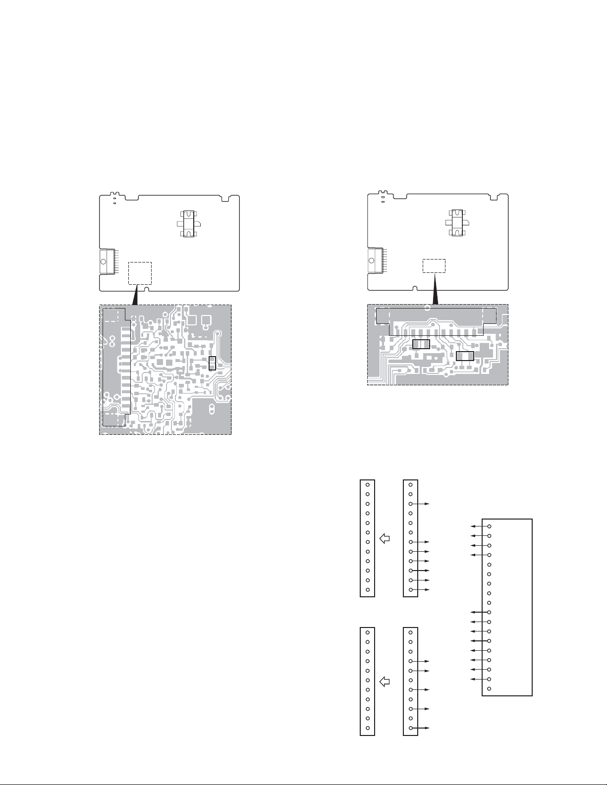
■ Terminal Function
Pin No. Name I/O Function
1 QT/DQT O QT/DQT output.
2 DTMF/MSK O DTMF/MSK/BEEP output
3 PLLE O PLL IC chip select.
4,5 NC I
6 GND - GND.
7 CNVSS - DNVss for flash.
8 EVLLD O E-volume LD.
9 BSHIFT O Beat shift.
10 RESET - Reset.
11 XOUT - X’tal (14.318MHz).
12 VSS - GND.
13 XIN - X’tal (14.318MHz).
14 VCC - +5V.
15 GND - GND (Input only).
16 NC I
17 POWER I Power key input.
18 INT I µcom stop.
19 NC I
20 TX/RX O TX/RX.
21 UL O PLL unlock detect.
22~25 NC I
26 EEPWP O EEPROM write protect
27 EEPCK O EEPROM clock (N ch open drain).
28 EEPDT I/O EEPROM data (N ch open drain).
29 FNC1 I/O Function P1/TxD for flash.
30 FNC2 I/O Function P2/RxD for flash.
31 CLKFLS I SCLK for flash.
32 BSYFLS O Busy for flash.
33 TXD O To FPU.
34 RXD I From FPU.
35 PTT I PTT key.
36 HOOK I Hook.
37,38 NC I
39 EMPFLS I/O EPM for flash.
40~42 NC I
43 FNC3 I/O Function port 3.
44 CEFLS I/O CE for flash.
45,46 FNC4, FNC5 I/O Function port 4, 5
47,48 FNC7, FNC6 I/O Function port 7, 6.
49 FNC8 I/O Function port 8.
50 AFM O AF mute.
51 SPM O Speaker mute.
Pin No. Name I/O Function
52 AMPSW O AF AMP switch.
53 DT O Common data.
54 CK O Common clock.
55,56 NC I
57~59 DST1~DST3 I Destination 1~3
60 VCC - +5V.
61 NC I
62 VSS - GND.
63 NC I
64 NARROW O
65 WIDE O
66~68 NC I
69 CL O Clock for LCD.
70 CE O Chip enable for LCD.
71 DI O Transfer data to LCD.
72 IGN I Ignition.
73 MICMT1 O Mic 1 mute.
74 MICEM O Mic 2 mute.
75 MICMT2 O Mic 3 mute.
76 8RC O 8R control.
77 8TC O 8T control.
78 CM I/O Mic key check.
79~81 NC I
82 SBC O Battery switch.
83 KMI2 I Key matrix 2.
84 KMI1 I Key matrix 1.
85 KMI3 I Key matrix 3.
86 KMI4 I Key matrix 4.
87 NC I
88 SIGNAL I DTMF/QT/DQT input.
89 TEMP2 I Temperature 2.
90 TEMP1 I Temperature 1.
91 BATT I Battery voltage.
92 RSSI I RSSI input.
93 SQIN I Squelch input.
94 AVSS - GND.
95 NC I
96 VREF - +5V.
97 AVCC - +5V.
98 NC I
99 KMO1 O Key matrix output 1.
100 KMO2 O Key matrix output 2.
TK-7102H
19

TK-7102H
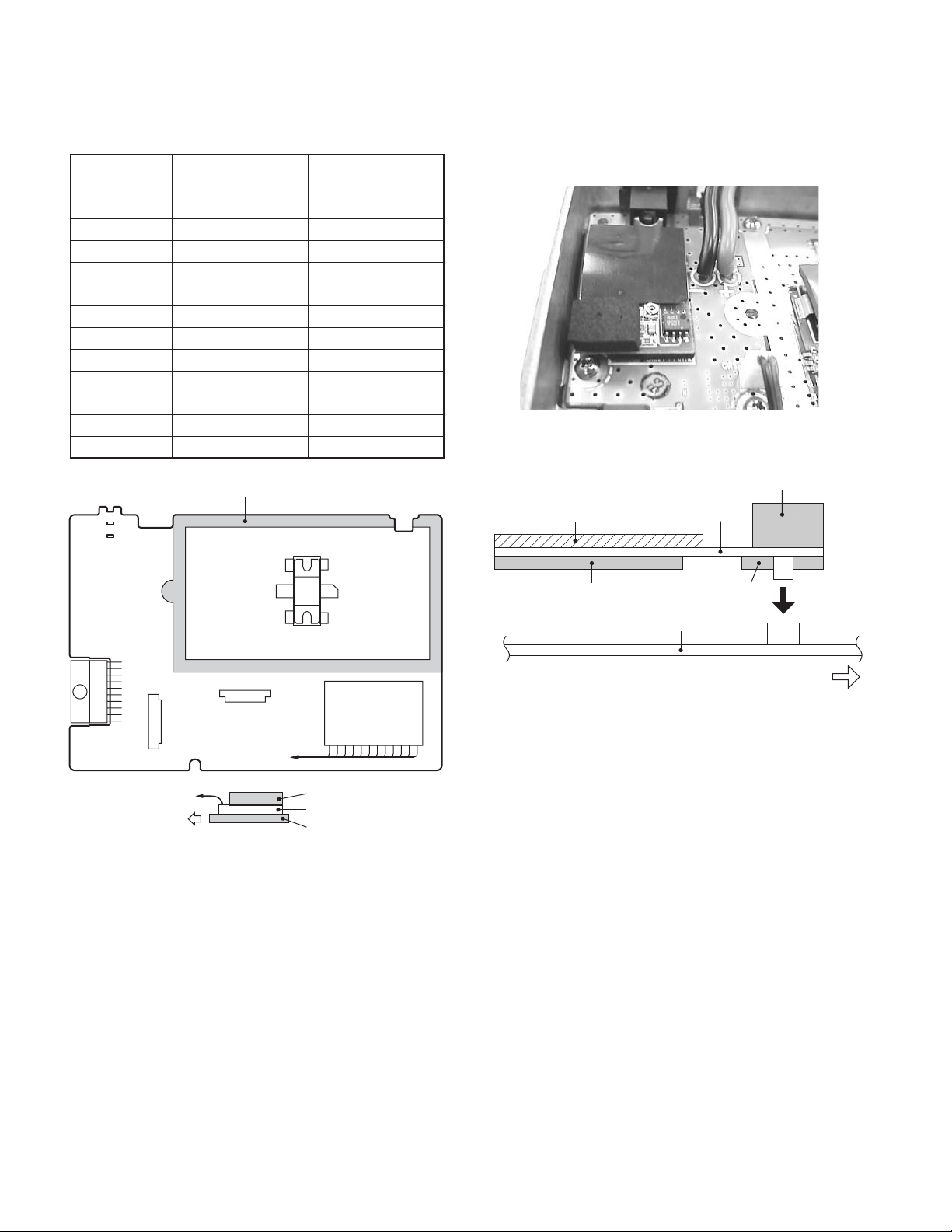
COMPONENTS DESCRIPTION
Display Unit (X54-3460-20)
Ref. No. Parts name Description
IC1 IC Shift register for LED & MICBL control
Q4 Transistor Busy light switch
Q9,10 Transistor Key backlit switch
D1~4 LED Key backlit
D5 LED Monitor key light
D6 LED Programmable key light
D7~10 LED Channel key light
D11 LED Busy
D12 LED Transmit
D13 Diode Surge protection
TX-RX Unit (X57-6700-XX)
Ref. No. Parts name Description
IC31 IC Voltage regulator (8C)
IC32 IC Voltage regulator (5C)
IC33 IC Voltage regulator (5M)
IC34 IC Voltage detector reset
IC35 IC Voltage detector int
IC66 IC EEPROM
IC101 IC CPU
IC161 IC Digital potentiometer
IC201 IC MIC amplifier / IDC
IC202 IC MIC amplifier / Splatter filter
IC203 IC Buffer amplifier / SUM amplifier
/ DC amplifier / 1/2 Vcc
IC251 IC Audio filter
IC252 IC Audio amplifier
IC301 IC FM demodulation
IC401 IC PLL synthesizer
IC402 IC Divider (Hetero)
IC501 IC APC controller
Q1 FET TX AF
Q31,32 Transistor
Q33,34 Transistor DC switch (8R) / Active while RX
Q35,36 Transistor DC switch (8T) / Active while TX
Q61 Transistor Over voltage detection / Active when
Q71 Transistor Ignition / Ignition sens
Q86,87 Transistor Beat shift / Active while beat shift is on
Q201 Transistor
Q202 FET Emergency MIC mute / Active when
Q251 Transistor Buffer amplifier / RX audio
Q252,253
FET AF mute / Active while AFM is H
DC switch (SB) / Active when power is on
PS voltage is more than 18V
AF amplifier / MIC mute / Emergency MIC mute
MICEM is H
Ref. No. Parts name Description
Q254
Q255 Transistor AF mute / Active while AMPSW is H
Q301 Transistor Noise amplifier / SQL amplifier
Q302 Transistor Buffer amplifier / 16.8MHz 3rd over tone
Q351 Transistor IF amplifier
Q352 FET Mixer
Q353 FET RF amplifier / LNA
Q354 Transistor RF BPF
Q402,403
Q404 Transistor RF amplifier / PLL F in
Q405 FET RX VCO
Q406 FET TX VCO
Q407 FET T/R switch
Q408 Transistor T/R switch
Q410 Transistor Buffer amplifier / Output of VCO
Q411 Transistor RF amplifier / Output of VCO
Q440 Transistor Lipple filter
Q501,502
Q503 FET RF amplifier / Drive amplifier
Q504 FET RF amplifier / Final amplifier
D1 Diode Surge absorption / CM
D2 Diode Surge absorption / HOOK
D3 Diode Surge absorption / PTT
D4~11 Diode Surge absorption / FNC1~8
D31 Diode Reverse connection protection
D32 Poly switch Current protection
D61 Diode Over voltage detection
D201 Diode OR gate / MIC mute, AGC
D202 Diode AGC
D251 Diode Limiter
D301 Diode Detection
D302,303
D351~354
D401 Diode Lipple filter
D402 Diode Voltage dropped
D403,404
D405,406
D407 Varicap Modulation
D408 Diode Lipple filter
D409 Diode RF switch (TX/RX)
D501,502
D503 Diode Voltage protection
D602~605
D606,607
D608 Diode Temperature compensation
Digital transistor
Transistor Charge pump
Transistor RF amplifier / Drive stage
Diode IF switch (Wide/Narrow)
Varicap RF BPF tuning
Varicap RX VCO
Varicap TX VCO
Diode Temperature compensation
Diode ANT switch
Diode APC voltage detect
AF mute / Active while SPM is H
20

PARTS LIST
TK-7102H
✽ New Parts. indicates safety critical components.
Parts without Parts No. are not supplied.
Les articles non mentionnes dans le Parts No. ne sont pas fournis.
Teile ohne Parts No. werden nicht geliefert.
Ref. No.
Address
New
Parts No. Description
parts
TK-7102H
11BA01-2181-01 CABINET
23B✽ A10-4048-21 CHASSIS
33AA62-0942-03 PANEL ASSY
53A✽ B10-2753-03 FRONT GLASS
81D✽ B62-1596-10 INSTRUCTION MANUAL (ENGLISH)
91D✽ B62-1597-10 INSTRUCTION MANUAL (SPANISH)
10 3B ✽ B72-2036-14 MODEL NAME PLATE K
10 3B ✽ B72-2037-14 MODEL NAME PLATE K2
10 3B ✽ B72-2038-14 MODEL NAME PLATE M
10 3B ✽ B72-2039-14 MODEL NAME PLATE M2
12 3B E04-0167-05 RF COAXIAL PECEPTACLE (M)
14 3C E30-3339-05 DC CORD ACCESSORY
15 2B E30-3448-05 DC CORD (RADIO)
16 2A E37-1041-05 FLAT CABLE
- E37-1080-05 FOR SCRAMBLER BOARD (B)
- E37-1081-05 FOR SCRAMBLER BOARD (A)
19 3A E37-1082-05 SPEAKER CABLE
21 2B F10-2449-01 SHIELDING COVER
22 3C F51-0017-05 FUSE (6✽30) ACCESSORY
24 2B G02-0894-04 EARTH SPRING (FINAL FET)
- G10-1274-04 FIBROUS SHEET (PANEL ASSY)
25 3B ✽ G11-4127-14 RUBBER SHEET (CHASSIS)
26 2B G11-4240-04 RUBBER SHEET (DRIVE FET)
27 3B G13-1468-04 CUSHION (DC CORD)
28 3A G13-1836-04 CUSHION (SPEAKER)
- G13-1963-04 CUSHION (SCRAMBLER BOARD)
- G13-1964-04 CUSHION (SCRAMBLER BOARD)
- G13-1972-04 CUSHION (TRUNKING BOARD)
30 3A G53-1525-03 PACKING (PANEL)
31 2B G53-1542-03 PACKING (PHONE JACK)
32 1B G53-1544-01 PACKING (CABINET)
33 2A G53-1548-02 GASKET
35 2C,1D H12-3112-05 PACKING FIXTURE
36 3D H13-1190-02 CARTON BOARD
37 1D H25-2341-04 PROTECTION BAG
38 2D H52-1829-22 ITEM CARTON CASE
40 3C J19-1584-05 HOLDER ACCESSORY K,K2
41 3D J29-0662-03 BRACKET ACCESSORY
43 3A K29-9065-01 KEY TOP
A2BN67-2608-46 PAN HEAD SEMS SCREW W
B 2B,3B N87-2606-46 BRAZIER HEAD TAPTITE SCREW
C 1B,2B N87-2614-46 BRAZIER HEAD TAPTITE SCREW
45 3C N99-0395-05 SCREW SET ACCESSORY
47 3A T07-0739-05 SPEAKER
48 2C T91-0624-05 MICROPHONE ACCESSORY K,K2
Destination
L : Scandinavia K : USA P : Canada
Y : PX (Far East, Hawaii) T : England E : Europe
Y : AAFES (Europe) X : Australia M :Other Areas
TK-7102H
DISPLAY UNIT (X54-3460-20)
TX-RX UNIT (X57-6700-XX)
Ref. No.
D11 B30-2237-05 LED (YG)
D12 B30-2240-05 LED (SR)
C4 CK73GB1H103K CHIP C 0.010UF K
C8-17 CK73GB1H103K CHIP C 0.010UF K
C18 CK73GB1A105K CHIP C 1.0UF K
C25 CK73GB1H103K CHIP C 0.010UF K
C27 CK73GB1C104K CHIP C 0.10UF K
CN1 E40-6005-05 FLAT CABLE CONNECTOR
J1 E08-0877-05 MODULAR JACK
L1 L92-0138-05 FERRITE CHIP
CP3,4 RK75GB1J392J CHIP-COM 3.9K J 1/16W
R1-6 RK73GB1J102J CHIP R 1.0K J 1/16W
R7-15 RK73FB2A272J CHIP R 2.7K J 1/10W
R16 RK73GB1J101J CHIP R 100 J 1/16W
R17 RK73GB1J100J CHIP R 10 J 1/16W
R18 RK73GB1J472J CHIP R 4.7K J 1/16W
R19,20 RK73GB1J222J CHIP R 2.2K J 1/16W
D13 DA221 DIODE
IC1 BU2090FS MOS IC
Q4 KRC102S DIGITAL TRANSISTOR
Q9 KRA225S DIGITAL TRANSISTOR
Q10 KRC102S DIGITAL TRANSISTOR
Address
New
Parts No. Description
parts
Destination
TX-RX UNIT (X57-6700-XX) -22 : M -23 : M2 -24 : K -25 : K2
C10 CK73GB1H102K CHIP C 1000PF K
C13-26 CK73GB1H471K CHIP C 470PF K
C28 CK73GB1H221K CHIP C 220PF K
C29 CK73GB1H471K CHIP C 470PF K
C30 CK73GB1H102K CHIP C 1000PF K
C33 CK73GB1H102K CHIP C 1000PF K
C34 C92-0721-05 CHIP-ELE 330UF 25WV
C35-38 CK73GB1H102K CHIP C 1000PF K
C39,40 CK73GB1C104K CHIP C 0.10UF K
C41 C92-0795-05 CHIP-TAN 22UF 10WV
C42 CK73GB1H103K CHIP C 0.010UF K
C43-45 C92-0795-05 CHIP-TAN 22UF 10WV
C49,50 CK73GB1H103K CHIP C 0.010UF K
C51 C92-0560-05 CHIP-TAN 10UF 6.3WV
C52,53 CK73GB1H102K CHIP C 1000PF K
C54,55 CK73GB1C104K CHIP C 0.10UF K
C56 CK73GB1H102K CHIP C 1000PF K
C61 CK73GB1H102K CHIP C 1000PF K
C66 CK73GB1H102K CHIP C 1000PF K
C72 CK73GB1H102K CHIP C 1000PF K
C77,78 CK73GB1H102K CHIP C 1000PF K
C82 CK73GB1H102K CHIP C 1000PF K
C83 CK73GB1C104K CHIP C 0.10UF K
C87 CC73GCH1H180J CHIP C 18PF J
C88,89 CC73GCH1H060B CHIP C 6.0PF B
DISPLAY UNIT (X54-3460-20)
D1-4 B30-2238-05 LED (Y)
D5-10 B30-2239-05 LED (SY)
C90 CC73GCH1H180J CHIP C 18PF J
C97,98 CK73GB1H102K CHIP C 1000PF K
C101 CK73GB1H102K CHIP C 1000PF K
C102 CK73GB1C104K CHIP C 0.10UF K
21

TK-7102H
TX-RX UNIT (X57-6700-XX)
Ref. No.
C103 CK73GB1H102K CHIP C 1000PF K
C104 CK73GB1C104K CHIP C 0.10UF K
C151 CK73GB1H182K CHIP C 1800PF K
C152 CK73GB1H392K CHIP C 3900PF K
C161 CK73GB1H102K CHIP C 1000PF K
Address
New
Parts No. Description
parts
PARTS LIST
Destination
Ref. No.
Address
C301 C92-0507-05 CHIP-TAN 4.7UF 6.3WV
C302 CK73GB1H102K CHIP C 1000PF K
C303 CK73GB1H472K CHIP C 4700PF K
C304,305 CC73GCH1H331J CHIP C 330PF J K,M
C304,305 CC73GCH1H391J CHIP C 390PF J K2,M2
New
Parts No. Description
parts
Destination
C162 C92-0507-05 CHIP-TAN 4.7UF 6.3WV
C163 CK73GB1H102K CHIP C 1000PF K
C164 C92-0560-05 CHIP-TAN 10UF 6.3WV
C201 CK73GB1C104K CHIP C 0.10UF K
C202 CK73GB1H102K CHIP C 1000PF K
C203 CK73GB1C273K CHIP C 0.027UF K
C204 C92-0514-05 CHIP-TAN 2.2UF 10WV
C205 CK73GB1C104K CHIP C 0.10UF K
C206 CK73GB1H102K CHIP C 1000PF K
C207 CK73GB1C223K CHIP C 0.022UF K
C208 CK73GB1H103K CHIP C 0.010UF K
C210 CK73GB1C104K CHIP C 0.10UF K
C211 CK73GB1H821K CHIP C 820PF K
C212 CK73GB1H122K CHIP C 1200PF K
C213 CK73GB1H332K CHIP C 3300PF K
C214 CC73GCH1H151J CHIP C 150PF J
C215 CK73GB1C104K CHIP C 0.10UF K
C217,218 C92-0560-05 CHIP-TAN 10UF 6.3WV
C220 C92-0507-05 CHIP-TAN 4.7UF 6.3WV
C221 CK73GB1C104K CHIP C 0.10UF K
C225 C92-0004-05 CHIP-TAN 1.0UF 16WV
C226 CK73GB1H472K CHIP C 4700PF K
C227 CK73GB1E103K CHIP C 0.010UF K
C228 C92-0560-05 CHIP-TAN 10UF 6.3WV
C229 C92-0507-05 CHIP-TAN 4.7UF 6.3WV
C230 CK73GB1C104K CHIP C 0.10UF K
C231,232 CK73GB1H102K CHIP C 1000PF K
C233 C92-0507-05 CHIP-TAN 4.7UF 6.3WV
C250 CK73GB1C104K CHIP C 0.10UF K
C251 C92-0714-05 CHIP-TAN 4.7UF 6.3WV
C306 CK73GB1H102K CHIP C 1000PF K
C307 CK73GB1E223K CHIP C 0.022UF K
C308 CK73GB1H102K CHIP C 1000PF K
C309 CK73GB1E223K CHIP C 0.022UF K
C310 CK73FB1C334K CHIP C 0.33UF K
C311,312 CK73GB1C104K CHIP C 0.10UF K
C313 C92-0662-05 CHIP-TAN 15UF 6.3WV
C314 CK73GB1H103K CHIP C 0.010UF K
C315-318 CK73GB1C104K CHIP C 0.10UF K
C319 CC73GCH1H101J CHIP C 100PF J
C322 CC73GCH1H560J CHIP C 56PF J
C323 CC73GCH1H271J CHIP C 270PF J
C324 CK73GB1H103K CHIP C 0.010UF K
C326 CK73GB1H103K CHIP C 0.010UF K
C350 CK73GB1H471K CHIP C 470PF K
C351 CC73GCH1H330J CHIP C 33PF J
C353 CK73GB1H103K CHIP C 0.010UF K
C355 CC73GCH1H150J CHIP C 15PF J
C357 CK73GB1H103K CHIP C 0.010UF K
C358 CK73GB1H102K CHIP C 1000PF K
C359 CC73GCH1H080B CHIP C 8.0PF B
C360-362 CK73GB1H102K CHIP C 1000PF K
C363 CK73GB1H103K CHIP C 0.010UF K
C364 CK73GB1H102K CHIP C 1000PF K
C366 CK73GB1C104K CHIP C 0.10UF K
C367 CC73GCH1H101J CHIP C 100PF J K,M
C367 CC73GCH1H151J CHIP C 150PF J K2,M2
C368 CC73GCH1H220J CHIP C 22PF J
C369 CC73GCH1H0R5B CHIP C 0.5PF B K2,M2
C369 CC73GCH1H040B CHIP C 4.0PF B K,M
C252 CC73GCH1H390J CHIP C 39PF J
C253,254 CK73GB1A105K CHIP C 1.0UF K
C255 CK73GB1H822K CHIP C 8200PF K
C256 CK73GB1E183K CHIP C 0.018UF K
C257 CK73GB1C393K CHIP C 0.039UF K
C258-261 CK73GB1H103J CHIP C 0.010UF J
C262 CK73GB1H102K CHIP C 1000PF K
C263,264 CK73GB1C333K CHIP C 0.033UF K
C265,266 CK73GB1C104K CHIP C 0.10UF K
C267 CK73GB1A474K CHIP C 0.47UF K
C268 CK73GB1C104K CHIP C 0.10UF K
C269 CK73GB1A105K CHIP C 1.0UF K
C270 C92-0507-05 CHIP-TAN 4.7UF 6.3WV
C271 CK73GB1H332K CHIP C 3300PF K
C272 CK73GB1H102K CHIP C 1000PF K
C273 CK73GB1A105K CHIP C 1.0UF K
C274 CK73FB1C224K CHIP C 0.22UF K
C275 CK73GB1A105K CHIP C 1.0UF K
C276,277 CK73GB1H102K CHIP C 1000PF K
C278 CK73GB1C104K CHIP C 0.10UF K
C279 C92-0516-05 CHIP-TAN 4.7UF 16WV
C280 C92-0040-05 CHIP-ELE 47UF 16WV
C281 CK73GB1H102K CHIP C 1000PF K
C282 C92-0722-05 CHIP-ELE 470UF 16WV
C283 CK73GB1H102K CHIP C 1000PF K
22
C370 CK73GB1H102K CHIP C 1000PF K
C371 CC73GCH1H020B CHIP C 2.0PF B
C372 CK73GB1H102K CHIP C 1000PF K
C373 CC73GCH1H040B CHIP C 4.0PF B K,M
C374 CC73GCH1H220J CHIP C 22PF J
C375-380 CK73GB1H102K CHIP C 1000PF K
C382 CC73GCH1H220J CHIP C 22PF J
C383 CK73GB1H102K CHIP C 1000PF K
C384 CC73GCH1H010B CHIP C 1.0PF B
C386 CC73GCH1H240J CHIP C 24PF J K,M
C386 CC73GCH1H270J CHIP C 27PF J K2,M2
C387 CK73GB1H102K CHIP C 1000PF K
C388 CC73GCH1H040B CHIP C 4.0PF B K,M
C388 CC73GCH1H060B CHIP C 6.0PF B K2,M2
C389 CK73GB1H102K CHIP C 1000PF K
C401-403 CC73GCH1H101J CHIP C 100PF J
C404 C92-0662-05 CHIP-TAN 15UF 6.3WV
C406 CK73GB1H102K CHIP C 1000PF K
C408 CC73GCH1H220J CHIP C 22PF J
C409 CK73GB1C104K CHIP C 0.10UF K
C410 C92-0560-05 CHIP-TAN 10UF 6.3WV
C411 CK73GB1C104K CHIP C 0.10UF K
C412 C92-0560-05 CHIP-TAN 10UF 6.3WV
C413 CK73GB1H103K CHIP C 0.010UF K
C414 CK73GB1C104K CHIP C 0.10UF K

Ref. No.
C416-418 CK73GB1H102K CHIP C 1000PF K
C421,422 CK73GB1H471K CHIP C 470PF K
C423 C92-0555-05 CHIP-TAN 0.047UF 35WV
C424 C92-0004-05 CHIP-TAN 1.0UF 16WV
C425 C92-0001-05 CHIP C 0.1UF 35WV
Address
New
Parts No. Description
parts
PARTS LIST
Destination
Ref. No.
C526 CK73GB1H681K CHIP C 680PF K
C527 CK73GB1H102K CHIP C 1000PF K
C528 CK73GB1H221K CHIP C 220PF K
C529 CK73FB1H102K CHIP C 1000PF K
C530 CK73FB1C474K CHIP C 0.47UF K
Address
TK-7102H
New
Parts No. Description
parts
TX-RX UNIT (X57-6700-XX)
Destination
C426 CC73GCH1H120J CHIP C 12PF J K2,M2
C426 CC73GCH1H270J CHIP C 27PF J K,M
C427 CC73GCH1H040B CHIP C 4.0PF B K2,M2
C427 CC73GCH1H080B CHIP C 8.0PF B K,M
C428 CK73GB1H471K CHIP C 470PF K
C429 CC73GCH1H010B CHIP C 1.0PF B K,M
C429 CC73GCH1H020B CHIP C 2.0PF B K2,M2
C430,431 CC73GCH1H050B CHIP C 5.0PF B
C432 CC73GCH1H0R5B CHIP C 0.5PF B
C434 CC73GCH1H330J CHIP C 33PF J K2,M2
C434 CK73GB1H471K CHIP C 470PF K K,M
C435 CC73GCH1H050B CHIP C 5.0PF B K2,M2
C435 CC73GCH1H100C CHIP C 10PF C K,M
C436 CC73GCH1H0R5B CHIP C 0.5PF B
C437 CK73GB1H471K CHIP C 470PF K
C438 CC73GCH1H020B CHIP C 2.0PF B
C439 CC73GCH1H060B CHIP C 6.0PF B K,M
C439,440 CC73GCH1H060B CHIP C 6.0PF B K2,M2
C440 CC73GCH1H070B CHIP C 7.0PF B K,M
C441 CC73GCH1H0R5B CHIP C 0.5PF B
C442 C92-0560-05 CHIP-TAN 10UF 6.3WV
C444 CK73GB1H471K CHIP C 470PF K
C448,449 CK73GB1H471K CHIP C 470PF K
C450 C92-0568-05 CHIP-TAN 22UF 10WV
C451,452 CK73GB1H471K CHIP C 470PF K
C453 CK73GB1H221K CHIP C 220PF K
C454 CC73GCH1H060B CHIP C 6.0PF B
C455 CC73GCH1H030B CHIP C 3.0PF B
C456 CC73GCH1H020B CHIP C 2.0PF B
C457 CK73GB1H102K CHIP C 1000PF K
C531 C92-0719-05 CHIP-ELE 47UF 25WV
C533 C93-0570-05 CHIP C 68PF J K,M
C533 C93-0572-05 CHIP C 100PF J K2,M2
C536 CK73FB1H102K CHIP C 1000PF K
C541,542 CM73F2H270J CHIP C 27PF J K,M
C545 C93-0603-05 CHIP C 1000PF K
C546 CK73FB1C474K CHIP C 0.47UF K
C549 CM73F2H221J CHIP C 220PF J
C550 CM73F2H680J CHIP C 68PF J
C552 C93-0564-05 CHIP C 22PF J K2,M2
C552,553 C93-0562-05 CHIP C 15PF J K,M
C553 C93-0550-05 CHIP C 1.0PF C K2,M2
C554 C93-0603-05 CHIP C 1000PF K
C555 C93-0555-05 CHIP C 5.0PF C
C556 C93-0603-05 CHIP C 1000PF K
C557,558 CK73GB1H103K CHIP C 0.010UF K
C559 CK73GB1C104K CHIP C 0.10UF K
C560 CK73GB1H102K CHIP C 1000PF K
C574 CK73GB1H102K CHIP C 1000PF K
C576 CK73GB1H221K CHIP C 220PF K
C601 CC73GCH1H120J CHIP C 12PF J K,M
C601 CC73GCH1H180J CHIP C 18PF J K2,M2
C602 C93-0555-05 CHIP C 5.0PF C
C603 C93-0603-05 CHIP C 1000PF K
C605 C93-0564-05 CHIP C 22PF J K,M
C605 C93-0566-05 CHIP C 33PF J K2,M2
C606 CC73GCH1H0R5B CHIP C 0.5PF B
C607 CC73GCH1H020B CHIP C 2.0PF B
C608 C93-0566-05 CHIP C 33PF J
C610 CC73GCH1H0R5B CHIP C 0.5PF B
C458 CK73GB1H221K CHIP C 220PF K
C459 CK73GB1H102K CHIP C 1000PF K
C460 CC73GCH1H180J CHIP C 18PF J
C461 CK73GB1H102K CHIP C 1000PF K
C462 CC73GCH1H100C CHIP C 10PF C
C463,464 CK73GB1H102K CHIP C 1000PF K
C465 CC73GCH1H220J CHIP C 22PF J
C466 CC73GCH1H101J CHIP C 100PF J
C467 CK73GB1H102K CHIP C 1000PF K
C468 CK73GB1H221K CHIP C 220PF K
C471 CC73GCH1H100C CHIP C 10PF C K,M
C471 CC73GCH1H120J CHIP C 12PF J K2,M2
C501,502 CK73GB1H102K CHIP C 1000PF K
C503 CC73GCH1H101J CHIP C 100PF J
C504-507 CK73GB1H102K CHIP C 1000PF K
C509 CC73GCH1H150J CHIP C 15PF J
C510 CC73GCH1H080B CHIP C 8.0PF B
C511-514 CK73GB1H102K CHIP C 1000PF K
C515 CC73GCH1H270J CHIP C 27PF J
C516 CK73GB1H821K CHIP C 820PF K
C517 CC73GCH1H030B CHIP C 3.0PF B
C518 CC73GCH1H330J CHIP C 33PF J
C519 CC73GCH1H820J CHIP C 82PF J
C522 CK73FB1H102K CHIP C 1000PF K
C525 CK73GB1H102K CHIP C 1000PF K
C611 CC73GCH1H020B CHIP C 2.0PF B
C613 C93-0566-05 CHIP C 33PF J
C615 C93-0564-05 CHIP C 22PF J
C616,617 CK73GB1H102K CHIP C 1000PF K
TC351 C05-0399-05 CERAMIC TRIMMER CAP (6PF)
TC352 C05-0245-05 CERAMIC TRIMMER CAP (10PF)
TC401,402 C05-0245-05 CERAMIC TRIMMER CAP (10PF)
J1 E11-0425-05 3.5D PHONE JACK (3P)
CN1 E40-6268-05 FLAT CABLE CONNECTOR
CN2 E40-5702-05 PIN ASSY
CN3 E40-6292-05 PIN ASSY
CN4 E40-5932-05 PIN ASSY SOCKET
CN5 E40-3246-05 PIN ASSY
CN601 E23-0486-05 TERMINAL
F501 F53-0108-05 FUSE (1.8A/50V)
CF301 L72-0993-05 CERAMIC FILTER
CF302 L72-0999-05 CERAMIC FILTER
L101 L92-0443-05 FERRITE CHIP
L201 L92-0443-05 FERRITE CHIP
L301 L34-4554-05 COIL
L302 L41-3385-08 SMALL FIXED INDUCTOR
L303,304 L40-3381-86 SMALL FIXED INDUCTOR (0.33UH)
L351 L41-8285-08 SMALL FIXED INDUCTOR
23

TK-7102H
PARTS LIST
TX-RX UNIT (X57-6700-XX)
Ref. No.
L352 L41-5685-08 SMALL FIXED INDUCTOR
L354-356 L34-4612-05 AIR-CORE COIL K,M
L354-356 L34-4613-05 AIR-CORE COIL K2,M2
L357 L34-4611-05 AIR-CORE COIL
L401 L92-0443-05 FERRITE CHIP
Address
New
Parts No. Description
parts
Destination
Address
New
Parts No. Description
parts
Ref. No.
R70 RK73GB1J473J CHIP R 47K J 1/16W
R71 RK73GB1J472J CHIP R 4.7K J 1/16W
R72 RK73GB1J105J CHIP R 1.0M J 1/16W
R73 RK73GB1J104J CHIP R 100K J 1/16W
R74 RK73GB1J473J CHIP R 47K J 1/16W
Destination
L403 L41-1005-08 SMALL FIXED INDUCTOR
L404 L92-0442-05 FERRITE CHIP
L405 L92-0443-05 FERRITE CHIP
L406,407 L40-2702-86 SMALL FIXED INDUCTOR (27UH) K,M
L406,407 L40-2785-92 SMALL FIXED INDUCTOR (270NH) K2,M2
L408 L40-2778-67 SMALL FIXED INDUCTOR (27NH) K,M
L408 L40-3978-67 SMALL FIXED INDUCTOR (39NH) K2,M2
L409-412 L40-2702-86 SMALL FIXED INDUCTOR (27UH) K,M
L409-412 L40-2785-92 SMALL FIXED INDUCTOR (270NH) K2,M2
L413 L40-3978-67 SMALL FIXED INDUCTOR (39NH) K,M
L413 L40-6878-67 SMALL FIXED INDUCTOR (68NH) K2,M2
L414 L40-2785-92 SMALL FIXED INDUCTOR (270NH) K2,M2
L414,415 L40-4791-86 SMALL FIXED INDUCTOR (4.7UH) K,M
L415 L40-1085-92 SMALL FIXED INDUCTOR (100NH) K2,M2
L416,417 L92-0443-05 FERRITE CHIP
L418 L40-6875-92 SMALL FIXED INDUCTOR (68NH) K2,M2
L418 L41-3375-06 SMALL FIXED INDUCTOR K,M
L419 L41-1085-06 SMALL FIXED INDUCTOR
L420 L41-1585-06 SMALL FIXED INDUCTOR
L421 L41-1085-06 SMALL FIXED INDUCTOR
L422 L41-5675-06 SMALL FIXED INDUCTOR
L501,502 L41-6875-08 SMALL FIXED INDUCTOR
L503,504 L41-2775-06 SMALL FIXED INDUCTOR
L505 L34-4606-05 AIR-CORE COIL K,M
L505 L34-4645-05 AIR-CORE COIL K2,M2
L506 L34-4693-05 AIR-CORE COIL
L507 L34-4732-05 AIR-CORE COIL
L508 L34-4669-05 AIR-CORE COIL
L509 L34-4667-05 AIR-CORE COIL
L601 L34-4668-05 AIR-CORE COIL
R75 RK73GB1J102J CHIP R 1.0K J 1/16W
R76 RK73GH1J183D CHIP R 18K D 1/16W
R77 RK73GH1J134D CHIP R 130K D 1/16W
R78 RK73GB1J102J CHIP R 1.0K J 1/16W
R81 RK73GB1J473J CHIP R 47K J 1/16W
R82 R92-1252-05 CHIP R 0 OHM J 1/16W
R86 R92-1252-05 CHIP R 0 OHM J 1/16W
R87 RK73GB1J102J CHIP R 1.0K J 1/16W
R91,92 RK73GB1J102J CHIP R 1.0K J 1/16W
R93,94 RK73GB1J562J CHIP R 5.6K J 1/16W
R101,102 RK73GB1J473J CHIP R 47K J 1/16W
R103-106 RK73GB1J102J CHIP R 1.0K J 1/16W
R107,108 RK73GB1J473J CHIP R 47K J 1/16W
R109 RK73GB1J152J CHIP R 1.5K J 1/16W
R110 RK73GB1J473J CHIP R 47K J 1/16W
R111 RK73GB1J102J CHIP R 1.0K J 1/16W
R112,113 RK73GB1J473J CHIP R 47K J 1/16W
R114-119 RK73GB1J102J CHIP R 1.0K J 1/16W
R120-123 R92-1252-05 CHIP R 0 OHM J 1/16W
R124 RK73GB1J473J CHIP R 47K J 1/16W
R125-128 RK73GB1J102J CHIP R 1.0K J 1/16W
R129 R92-1252-05 CHIP R 0 OHM J 1/16W
R130,131 RK73GB1J102J CHIP R 1.0K J 1/16W
R151 RK73GB1J103J CHIP R 10K J 1/16W
R152 RK73GB1J472J CHIP R 4.7K J 1/16W
R161 RK73GB1J122J CHIP R 1.2K J 1/16W
R162 RK73GB1J152J CHIP R 1.5K J 1/16W
R163 RK73GB1J473J CHIP R 47K J 1/16W
R164-166 RK73GB1J102J CHIP R 1.0K J 1/16W
R201 RK73GB1J681J CHIP R 680 J 1/16W
L602-604 L34-4670-05 AIR-CORE COIL
L605 L34-4667-05 AIR-CORE COIL
X86 L77-1934-05
X401 L77-1868-15 TCXO (16.8MHZ)
XF351 L71-0591-05 MCF (49.95MHZ)
R1 RK73GB1J101J CHIP R 100 J 1/16W
R2 R92-1252-05 CHIP R 0 OHM J 1/16W
R3 RK73GB1J102J CHIP R 1.0K J 1/16W
R4 RK73GB1J332J CHIP R 3.3K J 1/16W
R5 RK73GB1J223J CHIP R 22K J 1/16W
R31 RK73GB1J472J CHIP R 4.7K J 1/16W
R32 R92-1215-05 CHIP R 470 J 1/2W
R33 RK73GB1J473J CHIP R 47K J 1/16W
R34 RK73GB1J472J CHIP R 4.7K J 1/16W
R35 RK73GB1J473J CHIP R 47K J 1/16W
R36 RK73GB1J152J CHIP R 1.5K J 1/16W
R37 R92-1252-05 CHIP R 0 OHM J 1/16W
R38 RK73GB1J334J CHIP R 330K J 1/16W
R39 RK73GB1J474J CHIP R 470K J 1/16W
R40 RK73GB1J394J CHIP R 390K J 1/16W
R41 RK73GB1J334J CHIP R 330K J 1/16W
R61 RK73GB1J471J CHIP R 470 J 1/16W
R62 RK73GB1J102J CHIP R 1.0K J 1/16W
R66,67 RK73GB1J473J CHIP R 47K J 1/16W
R68,69 RK73GB1J102J CHIP R 1.0K J 1/16W
CRYSTAL RESONATOR (14.31818MHZ)
24
R202 R92-0670-05 CHIP R 0 OHM
R203 RK73GB1J104J CHIP R 100K J 1/16W
R204 RK73GB1J183J CHIP R 18K J 1/16W
R205 RK73GB1J821J CHIP R 820 J 1/16W
R206 RK73GB1J101J CHIP R 100 J 1/16W
R207 RK73GB1J754J CHIP R 750K J 1/16W
R208 RK73GB1J152J CHIP R 1.5K J 1/16W
R209 RK73GB1J244J CHIP R 240K J 1/16W
R210 RK73GB1J183J CHIP R 18K J 1/16W
R211,212 RK73GB1J823J CHIP R 82K J 1/16W
R213 RK73GB1J334J CHIP R 330K J 1/16W
R214,215 RK73GB1J683J CHIP R 68K J 1/16W
R216 RK73GB1J274J CHIP R 270K J 1/16W
R217 RK73GB1J224J CHIP R 220K J 1/16W
R218 RK73GB1J823J CHIP R 82K J 1/16W
R219 RK73GB1J184J CHIP R 180K J 1/16W
R220,221 RK73GH1J153D CHIP R 15K D 1/16W
R222 RK73GB1J102J CHIP R 1.0K J 1/16W
R223 RK73GB1J472J CHIP R 4.7K J 1/16W
R224 RK73GB1J102J CHIP R 1.0K J 1/16W
R225 RK73GB1J154J CHIP R 150K J 1/16W
R226 RK73GB1J104J CHIP R 100K J 1/16W
R227 RK73GB1J223J CHIP R 22K J 1/16W
R228 RK73GB1J103J CHIP R 10K J 1/16W
R229 RK73GB1J684J CHIP R 680K J 1/16W

Ref. No.
R230 RK73GB1J124J CHIP R 120K J 1/16W
R231 RK73GB1J683J CHIP R 68K J 1/16W
R232 RK73GB1J912J CHIP R 9.1K J 1/16W
R233 RK73GB1J682J CHIP R 6.8K J 1/16W
R249-251 RK73GB1J473J CHIP R 47K J 1/16W
Address
New
Parts No. Description
parts
PARTS LIST
Destination
Ref. No.
R355,356 RK73GB1J102J CHIP R 1.0K J 1/16W K2,M2
R356 RK73GB1J102J CHIP R 1.0K J 1/16W K,M
R358 RK73GB1J470J CHIP R 47 J 1/16W
R359 RK73GB1J224J CHIP R 220K J 1/16W
R360 RK73GB1J474J CHIP R 470K J 1/16W
Address
TK-7102H
New
Parts No. Description
parts
TX-RX UNIT (X57-6700-XX)
Destination
R252 RK73GB1J474J CHIP R 470K J 1/16W
R253 R92-1252-05 CHIP R 0 OHM J 1/16W
R254 RK73GB1J681J CHIP R 680 J 1/16W
R255,256 RK73GB1J562J CHIP R 5.6K J 1/16W
R257 RK73GB1J105J CHIP R 1.0M J 1/16W
R258 RK73GB1J272J CHIP R 2.7K J 1/16W
R259 RK73GB1J123J CHIP R 12K J 1/16W
R260 RK73GB1J224J CHIP R 220K J 1/16W
R261 RK73GB1J124J CHIP R 120K J 1/16W
R262 RK73GB1J183J CHIP R 18K J 1/16W
R263 RK73GH1J913D CHIP R 91K D 1/16W
R264 RK73GH1J124D CHIP R 120K D 1/16W
R265 RK73GH1J562D CHIP R 5.6K D 1/16W
R266 RK73GB1J562J CHIP R 5.6K J 1/16W
R267 R92-0670-05 CHIP R 0 OHM
R268 RK73GB1J102J CHIP R 1.0K J 1/16W
R269 RK73GB1J823J CHIP R 82K J 1/16W
R270 RK73GB1J272J CHIP R 2.7K J 1/16W
R271 RK73GB1J561J CHIP R 560 J 1/16W
R272 RK73GB1J152J CHIP R 1.5K J 1/16W
R273 RK73GB1J472J CHIP R 4.7K J 1/16W
R274,275 RK73GB1J153J CHIP R 15K J 1/16W
R276 RK73GB1J473J CHIP R 47K J 1/16W
R277 RK73GB1J683J CHIP R 68K J 1/16W
R278 RK73GB1J123J CHIP R 12K J 1/16W
R279 RK73GB1J472J CHIP R 4.7K J 1/16W
R280 RK73GB1J391J CHIP R 390 J 1/16W
R281 R92-0670-05 CHIP R 0 OHM
R301,302 RK73GB1J472J CHIP R 4.7K J 1/16W
R303 RK73GB1J223J CHIP R 22K J 1/16W
R361 RK73GB1J470J CHIP R 47 J 1/16W K,M
R361 RK73GB1J560J CHIP R 56 J 1/16W K2,M2
R362 RK73GB1J474J CHIP R 470K J 1/16W
R363 RK73GB1J154J CHIP R 150K J 1/16W
R364 R92-1252-05 CHIP R 0 OHM J 1/16W
R365 RK73GB1J104J CHIP R 100K J 1/16W
R366 RK73GB1J471J CHIP R 470 J 1/16W
R367 RK73GB1J470J CHIP R 47 J 1/16W
R368 RK73GB1J104J CHIP R 100K J 1/16W
R369 R92-1252-05 CHIP R 0 OHM J 1/16W
R370 RK73GB1J151J CHIP R 150 J 1/16W
R371 RK73GB1J474J CHIP R 470K J 1/16W
R372 RK73GB1J124J CHIP R 120K J 1/16W K2,M2
R372 RK73GB1J224J CHIP R 220K J 1/16W K,M
R373 RK73GB1J684J CHIP R 680K J 1/16W
R374 RK73GB1J124J CHIP R 120K J 1/16W K2,M2
R374 RK73GB1J184J CHIP R 180K J 1/16W K,M
R375,376 RK73GB1J104J CHIP R 100K J 1/16W
R378 RK73GB1J100J CHIP R 10 J 1/16W K2,M2
R378 R92-1252-05 CHIP R 0 OHM J 1/16W K,M
R379 RK73GB1J104J CHIP R 100K J 1/16W
R401-403 RK73GB1J102J CHIP R 1.0K J 1/16W
R404 RK73GB1J103J CHIP R 10K J 1/16W
R405 R92-1252-05 CHIP R 0 OHM J 1/16W
R407 RK73GB1J152J CHIP R 1.5K J 1/16W
R408 RK73GB1J100J CHIP R 10 J 1/16W
R409 RK73GB1J104J CHIP R 100K J 1/16W
R410 RK73GB1J103J CHIP R 10K J 1/16W K2,M2
R410 RK73GB1J822J CHIP R 8.2K J 1/16W K,M
R411 RK73GB1J562J CHIP R 5.6K J 1/16W
R304 RK73GB1J472J CHIP R 4.7K J 1/16W
R305 RK73GB1J182J CHIP R 1.8K J 1/16W
R306 RK73GB1J274J CHIP R 270K J 1/16W
R308 RK73GB1J334J CHIP R 330K J 1/16W
R309 RK73GB1J332J CHIP R 3.3K J 1/16W
R310 RK73GB1J102J CHIP R 1.0K J 1/16W
R311 RK73GB1J333J CHIP R 33K J 1/16W
R312 RK73GB1J473J CHIP R 47K J 1/16W
R313 RK73GB1J104J CHIP R 100K J 1/16W
R314 RK73GB1J222J CHIP R 2.2K J 1/16W
R315 RK73GB1J183J CHIP R 18K J 1/16W
R316 RK73GB1J223J CHIP R 22K J 1/16W
R317-320 RK73GB1J103J CHIP R 10K J 1/16W
R321 RK73GB1J223J CHIP R 22K J 1/16W
R322 RK73GB1J101J CHIP R 100 J 1/16W
R323 RK73GB1J224J CHIP R 220K J 1/16W
R324 R92-1252-05 CHIP R 0 OHM J 1/16W
R325 RK73GB1J333J CHIP R 33K J 1/16W
R349 RK73GB1J473J CHIP R 47K J 1/16W
R350 RK73GB1J273J CHIP R 27K J 1/16W
R351 RK73GB1J471J CHIP R 470 J 1/16W
R352 RK73GB1J101J CHIP R 100 J 1/16W
R353 RK73GB1J104J CHIP R 100K J 1/16W
R354 RK73GB1J331J CHIP R 330 J 1/16W
R355 RK73GB1J471J CHIP R 470 J 1/16W K,M
R412,413 RK73GB1J103J CHIP R 10K J 1/16W
R414 RK73GB1J471J CHIP R 470 J 1/16W
R415 R92-1252-05 CHIP R 0 OHM J 1/16W
R416 RK73GB1J471J CHIP R 470 J 1/16W
R417 RK73GB1J224J CHIP R 220K J 1/16W
R418,419 RK73GB1J102J CHIP R 1.0K J 1/16W
R420 RK73GB1J272J CHIP R 2.7K J 1/16W
R421 RK73GB1J152J CHIP R 1.5K J 1/16W
R422 RK73GB1J103J CHIP R 10K J 1/16W
R423 RK73GB1J331J CHIP R 330 J 1/16W K2,M2
R423,424 RK73GB1J221J CHIP R 220 J 1/16W K,M
R424 RK73GB1J221J CHIP R 220 J 1/16W K2,M2
R425,426 RK73GB1J473J CHIP R 47K J 1/16W
R427 RK73GB1J104J CHIP R 100K J 1/16W
R428 RK73GB1J473J CHIP R 47K J 1/16W
R429,430 RK73GB1J101J CHIP R 100 J 1/16W
R431 RK73GB1J104J CHIP R 100K J 1/16W
R432 RK73GB1J102J CHIP R 1.0K J 1/16W
R433 RK73GB1J472J CHIP R 4.7K J 1/16W
R434 R92-1252-05 CHIP R 0 OHM J 1/16W
R435 RK73GB1J101J CHIP R 100 J 1/16W
R436 RK73GB1J124J CHIP R 120K J 1/16W
R437 RK73GB1J102J CHIP R 1.0K J 1/16W
R438 RK73GB1J223J CHIP R 22K J 1/16W
R439 RK73GB1J473J CHIP R 47K J 1/16W
25

TK-7102H
TX-RX UNIT (X57-6700-XX)
Ref. No.
R440-442 RK73GB1J101J CHIP R 100 J 1/16W
R443 RK73GB1J222J CHIP R 2.2K J 1/16W
R444 RK73GB1J102J CHIP R 1.0K J 1/16W
R501 RK73GB1J102J CHIP R 1.0K J 1/16W
R502 RK73GB1J271J CHIP R 270 J 1/16W
Address
New
Parts No. Description
parts
PARTS LIST
Destination
Ref. No.
Address
D604,605 XB15A709 DIODE K2,M2
D605 XB15A709 DIODE K,M
D606,607 MA742 DIODE
D608 1SS355 DIODE
IC31 KIA7808AF ANALOG IC
New
Parts No. Description
parts
Destination
R503 RK73GB1J180J CHIP R 18 J 1/16W
R504 RK73GB1J271J CHIP R 270 J 1/16W
R505 RK73GB1J222J CHIP R 2.2K J 1/16W
R506 RK73GB1J103J CHIP R 10K J 1/16W
R507 RK73GB1J100J CHIP R 10 J 1/16W
R509 RK73GB1J220J CHIP R 22 J 1/16W
R510 RK73GB1J152J CHIP R 1.5K J 1/16W
R511 RK73FB2A470J CHIP R 47 J 1/10W
R512 RK73FB2A100J CHIP R 10 J 1/10W
R513 RK73FB2A222J CHIP R 2.2K J 1/10W
R514 R92-1217-05 CHIP R 0 OHM
R516 R92-0670-05 CHIP R 0 OHM
R518 RK73EB2B330J CHIP R 33 J 1/8W
R519 RK73GB1J333J CHIP R 33K J 1/16W
R520 RK73GB1J183J CHIP R 18K J 1/16W
R521 RK73GB1J101J CHIP R 100 J 1/16W
R522 RK73EB2B181J CHIP R 180 J 1/8W K,M
R522 RK73EB2B331J CHIP R 330 J 1/8W K2,M2
R523 RK73GB1J393J CHIP R 39K J 1/16W K,M
R523 RK73GB1J473J CHIP R 47K J 1/16W K2,M2
R524 R92-1215-05 CHIP R 470 J 1/2W
R525 RK73GB1J563J CHIP R 56K J 1/16W
R526 R92-1261-05 CHIP R 150 J 1/2W
R527 RK73GB1J224J CHIP R 220K J 1/16W
R528,529 RK73GB1J471J CHIP R 470 J 1/16W
R530 RK73GB1J102J CHIP R 1.0K J 1/16W
R531 RK73GB1J473J CHIP R 47K J 1/16W
R532,533 R92-1252-05 CHIP R 0 OHM J 1/16W
R601,602 RK73GB1J223J CHIP R 22K J 1/16W
R603 RK73GB1J473J CHIP R 47K J 1/16W
IC32,33 NJM78L05UA BI-POLAR IC
IC34,35 PST9140NR MOS IC
IC66 AT24C64N10SI18 ROM IC
IC101 30622MAA-B83GP MPU
IC161 M62363FP MOS IC
IC201 NJM2100V MOS IC
IC202 NJM2904V MOS IC
IC203 NJM2902V MOS IC
IC251 NJM2902V MOS IC
IC252 2B LA4600 AF POWER IC
IC301 TK14489V BI-POLAR IC
IC401 MB15A02 MOS IC
IC402 UPB1509GV BI-POLAR IC
IC501 TA75W01FU MOS IC
Q1 2SK1824 FET
Q31 2SA1641(S,T) TRANSISTOR
Q32 KRC102S DIGITAL TRANSISTOR
Q33 2SA1745(6,7) TRANSISTOR
Q34 KRC102S DIGITAL TRANSISTOR
Q35 KTA1664(Y) TRANSISTOR
Q36 KRC102S DIGITAL TRANSISTOR
Q61 KRC404RTK DIGITAL TRANSISTOR
Q71 KRC414RTK DIGITAL TRANSISTOR
Q86,87 2SK1824 FET
Q201 2SC4919 TRANSISTOR
Q202 2SJ243 FET
Q251 2SC4617(S) TRANSISTOR
Q252,253 2SK1824 FET
Q254 DTC363EU DIGITAL TRANSISTOR
Q255 KRC102S DIGITAL TRANSISTOR
R605 RK73GB1J153J CHIP R 15K J 1/16W
R606 RK73GB1J221J CHIP R 220 J 1/16W
VR1 R12-6427-05 TRIMMING POT. (47K)
D1-11 DA221 DIODE
D31 ZSH5MA27 SURGE ABSORBER
D32 1812L110PR VARISTOR
D61 02DZ18(X,Y) ZENER DIODE
D201 DAN222 DIODE
D202 1SS372 DIODE
D251 MA742 DIODE
D301 MA742 DIODE
D302,303 DAN222 DIODE
D351-354 HVC350B VARIABLE CAPACITANCE DIODE
D401 MA2S111 DIODE
D402 HZU5ALL DIODE
D403-406 MA2S304 VARIABLE CAPACITANCE DIODE
D407 MA360 VARIABLE CAPACITANCE DIODE
D408 MA2S111 DIODE
D409 DAN235E DIODE
D501 1SS355 DIODE
D502 DA221 DIODE
D503 02DZ5.1(Y) ZENER DIODE
D602 MA4PH633 DIODE
D603 XB15A709 DIODE K,M
26
Q301 2SC2412K TRANSISTOR
Q302 2SC4617(S) TRANSISTOR
Q351 2SC5108(Y) TRANSISTOR
Q352,353 3SK255 FET
Q354 2SK1824 FET
Q402 2SA1832(GR) TRANSISTOR
Q403 2SC4738(GR) TRANSISTOR
Q404 2SC4649(N,P) TRANSISTOR
Q405,406 2SK508NV(K52) FET
Q407 2SJ243 FET
Q408 KRX102U TRANSISTOR
Q410 2SC5108(Y) TRANSISTOR
Q411 2SC4649(N,P) TRANSISTOR
Q440 2SC4617(S) TRANSISTOR
Q501,502 2SC3357 TRANSISTOR
Q503 PD55003TR FET
Q504 2B RD70HVF1-01 RF POWER FET
TH97,98 B57331V2104J THERMISTOR
TH301 B57331V2104J THERMISTOR
TH351 B57331V2104J THERMISTOR K2,M2
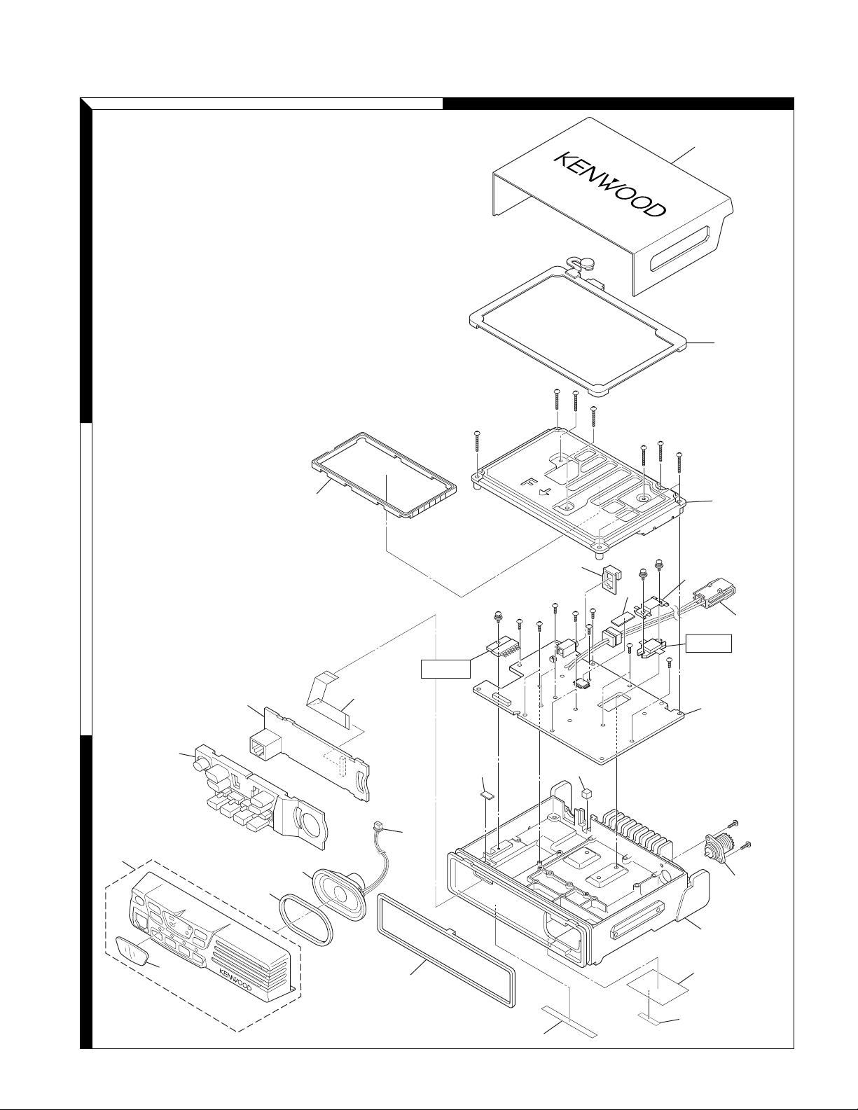
EXPLODED VIEW
TK-7102H
A
B
1
A M2.6 x 8 : N67-2608-46
B M2.6 x 6 (Br-Tap) : N87-2606-46
C M2.6 x 14 (Br-Tap) : N87-2614-46
1
32
C
C
C
33
C
C
C
Cx2
21
A
26
A
24
31
2
A
Bx12
15
Q504
IC252
Display unit
16
TX-RX unit
43
25
19
3
3
47
28
27
B
B
12
2
5
30
700
Caution label
Parts with the exploded numbers larger than 700 are not supplied.
10
701
S/No. label
27

TK-7102H
PACKING
C
8 Instruction manual (English)
(B62-1596-10)
37 Protection bag
(H25-2341-04)
1
37 Protection bag
(H25-2341-04)
35 Packing fixture
(H12-3112-05)
48 Microphone
(T91-0624-05) : K,K2
D
703 Pamphlet
702 Pamphlet
9 Instruction manual (Spanish)
(B62-1597-10)
35 Packing fixture
(H12-3112-05)
2
38 Item carton cse
(H52-1829-22)
45 Screw set
(N99-0395-05)
14 DC cord
(E30-3339-05)
41 Bracket
3
22 Fuse (6x30)
(F51-0017-05) x 2
40 Holder
(J19-1584-05) : K,K2
36 Carton board
(H13-1190-02)
(J29-0662-03)
28
Parts with the exploded numbers larger than 700 are not supplied.

ADJUSTMENT
Test Equipment Required for Alignment
Test Equipment Major Specifications
1. Standard Signal Generator Frequency Range 136 to 175MHz
(SSG) Modulation Frequency modulation and external modulation
Output –127dBm/0.1µV to greater than –7dBm/100mV
2. Power Meter Input Impedance 50Ω
Operation Frequency 136 to 175MHz or more
Measurement Capability Vicinity of 100W
3. Deviation Meter Frequency Range 136 to 175MHz
4. Digital Volt Meter Measuring Range 1 to 20V DC
(DVM) Accuracy High input impedance for minimum circuit loading
5. Oscilloscope DC through 30MHz
6. High Sensitivity Frequency Range 10Hz to 1000MHz
Frequency Counter Frequency Stability 0.2ppm or less
7. Ammeter 20A
8. AF Volt Meter Frequency Range 50Hz to 10kHz
(AF VTVM) Voltage Range 1mV to 3V
9. Audio Generator (AG) Frequency Range 20Hz to 20kHz or more
Output 0 to 1V
10. Distortion Meter Capability 3% or less at 1kHz
Input Level 50mV to 10Vrms
11. 4Ω Dummy Load Approx. 4Ω, 10W or more
12. Regulated Power Supply 13.6V, approx. 20A (adjustable from 9 to 17V)
Useful if ammeter requipped
13. Spectrum Analyzer Center frequency 50KHz to 600MHz
14. Tracking Generator Output Voltage 100mV or more
TK-7102H
Test cable for microphone input (E30-3360-08)
GREEN
1
RED
2
BLACK
3
BLUE
4
SHIELD
5
WHITE
6
GRAY
7
YELLOW
8
E
PTT
MIC-E
MIC
HK
MIC connector
(Front view)
1
8
1 : BLC
2 : PSB
3 : E
4 : PTT
5 : ME
6 : MIC
7 : HOOK
8 : CM
Tuning cable (E30-3383-05)
1
2
3
4
5
6
7
8
Adapter cable (E30-3383-05) is required for
injecting an audio if PC tuning is used.
See “PC Mode” section for the connection.
Lead wire +
Shield wire –
MIC
29

TK-7102H
ADJUSTMENT
Adjustment Location
■ Switch
Power
Volume
up/down
MIC jack
■ Adjustment Points
TX-RX unit
Component side
5M
IC252
RESET
+B
E
CNVSS
RXD
Display
1/2/3/4 keys
Q503
R518
R516
RF
POWER
TXD
DC
CV
key
F501
R524
8T
key
IGN
PC
Q504
VR1
BPF
Speaker
TEMP1
AFV
8T
TEMP2
■ Notes
• EEPROM
The tuning data (Deviation, Squelch, etc.) for the EEPROM, is stored in memory. When parts are changed, readjust the transceiver.
• AF PA IC (IC252)
How to mounting the IC252.
Pin 1 marker
IC252
Part name label face down
TX-RX UNIT
Component side
• Speaker Cable
The speaker cable should be formed before mounting the
shield cover as below.
ANT
TC352
TC351
BPF
L301
Speaker
cable
Locator
E+B
TX-RX unit
Foil side
TC401
TC402
• Fuse
To mount the fuse, the cable terminal direction must be as
follow.
This side up This side up
Fuse
Cable terminal Cable terminal
30

TK-7102H
ADJUSTMENT
Test Frequency (MHz)
Channel
1 : Center 160.100 160.050 149.100 149.050
2 : Low 146.100 146.050 136.100 136.050
3 : High 173.900 173.950 161.900 161.950
4 160.000 160.000 149.000 149.000
5 160.200 160.200 149.200 149.200
6 160.400 160.400 149.400 149.400
PCB Section
Item Condition
1. Setting 1) Power supply voltage
DC Power supply terminal : 13.6V
2. VCO lock 1) CH : TX high Digital voltmeter CV TC402 5.5V ±0.1V
voltage*
2) CH : RX high TC401 5.5V ±0.1V
K,M K2,M2
TX RX TX RX
Measurement
Test equipment
Terminal
Adjustment
Parts Method
Specifications/
Remarks
3) CH : TX low Check 0.7V or more
4) CH : RX low
3. IF coil 1) CH : RX center (Wide) SSG AFV L301 3.25~3.35V (DC)
4. RF 1) CH : RX center (Wide) Tra generator ANT TC351 Adjust the BPF waveform
bandpass CH : RX low (Wide) Spectrum analyzer BPF TC352 to Fig. 1
filter CH : RX high (Wide)
2) SSG output : –53dBm (501µV) Digital voltmeter
Mod : 1kHz
Dev : 3kHz
2) Tra generator output : –30dBm
Connect the spectrum analyzer
to BPF terminal
* Adjustment of TX VCO lock voltage
1. Remove R516, F501, R518 and R524 (all on component side).
2. Remove PCB from chassis.
3. Transmit and check voltage at [CV] point.
Warning : Do not transmit if step “1.” is not complete.
4. Adjust of voltage can be done by tuning TC402.
K,M
Fig. 1
K2,M2
31

TK-7102H
ADJUSTMENT
Receiver Section
Item Condition
1. Seisitivity 1) CH : RX low (Wide/Narrow) SSG ANT Check SINAD
CH : RX center (Wide/Narrow) Oscilloscope EXT. SP : 12dB or higher
CH : RX high (Wide/Narrow) AF V.M
2) SSG output Distortion meter
: –118dBm (0.28µV) (Wide)
: –116dBm (0.35µV) (Narrow)
Mod : 1kHz
Dev : ±3.0kHz (Wide)
Dev : ±1.5kHz (Narrow)
Measurement
Test equipment
Terminal
Parts Method
Adjustment
Specifications/
Remarks
2. Squelch 9 1) CH : RX low (Wide) PC key Adjust to open the squelch
3. Squelch 1 1) CH : RX low (Wide)
CH : RX center (Wide/Narrow)
CH : RX high (Wide)
2) SSG output
: –115dBm (0.4µV) (Wide)
: –114dBm (0.45µV) (Narrow)
Mod : 1kHz
Dev : ±3.0kHz (Wide)
Dev : ±1.5kHz (Narrow)
CH : RX center (Wide/Narrow)
CH : RX high (Wide)
2) SSG output
: –120dBm (0.22µV) (Wide)
: –119dBm (0.25µV) (Narrow)
Mod : 1kHz
Dev : ±3.0kHz (Wide)
Dev : ±1.5kHz (Narrow)
Transmitter Section
Item Condition
1. Frequency 1) CH : TX center Frequency counter ANT PC key Adjust to center frequency Within ±100Hz
2) Transmit
Measurement
Test equipment
Terminal
Parts Method
Adjustment
Specifications/
Remarks
2. Maximum 1) CH : TX high Power meter VR1 53W ± 1W
power 2) Transmit Hex data 255
limitting
3. High 1) CH : TX low PC key 50W ± 1.0W
power CH : TX low’
4. Low 1) CH : TX low 25W ± 1.0W
power CH : TX low’
CH : TX center
CH : TX high’
CH : TX high
2) Transmit
CH : TX center
CH : TX high’
CH : TX high
2) Transmit
32

ADJUSTMENT
TK-7102H
Item Condition
5. DQT 1) CH : TX low (Wide) Modulation analyzer ANT PC key
balance CH : TC center (Wide/Narrow) or Linear detector
CH : TX high (Wide) (LPF : 3kHz)
2) Transmit Oscilloscope
6. MAX 1) CH : TX low (Wide) Modulation analyzer ANT ±4.0kHz (Wide) ±50Hz
balance CH : TC center (Wide/Narrow) or Linear detector MIC ±2.0kHz (Narrow)
CH : TX high (Wide) (LPF : 15kHz) According to the large +, –
2) AG : 1kHz/50mV Oscilloscope
3) Transmit AG
7. MIC 1) CH : TX center (Wide/Narrow) Check ±3kHz±0.2kHz
sensitivity 2) AG : 1kHz/5mV (Wide)
3) Transmit ±1.5kHz±0.1kHz
8. DQT 1) CH : TX low (Wide) Modulation analyzer ± 0.75kHz (Wide) ± 0.05kHz
deviation CH : TX center (Wide/Narrow) or Linear detector ±0.35kHz (Narrow)
CH : TX high (Wide) (LPF : 3kHz)
2) Transmit Oscilloscope
9. QT 1) CH : TX low (Wide) ±0.75kHz (Wide) ±0.05kHz
deviation CH : TX center (Wide/Narrow) ±0.35kHz (Narrow)
CH : TX high (Wide)
2) Transmit
10. DTMF 1) CH : TX center (Wide/Narrow) ±3.0kHz (Wide) ± 0.2kHz
/MSK 2) Transmit ±1.5kHz (Narrow)
deviation
Measurement
Test equipment
AF V.M
Terminal
Parts Method
Adjustment
Adjust the waveform as below
Specifications/
Remarks
(Narrow)
If normal power is not obtained, please follow the
step below
Open the shielding cover (upper), and screw 3 locations
around ANT pin.
1. Switch off the transceiver.
Impedance of Final FET (Q504) and Drive FET (Q503) can
be measured easily using DVM Ω mode.
Normal condition – Gate : 20kΩ~50kΩ, Drain : 1MΩ~2MΩ
The above impedance values are rough estimations.
2. Switch on the transceiver. Check the voltage at F501 output point.
The voltage is around 13.6V in receiving condition. The
voltage will be 12.6V~ in transmitting condition. If found
0V at this point then F501 is broken.
3. Remove R516.
4. Connect 50Ω load at the ANT location.
Transmit and check current drain at High power mode.
If the current drain is less than 1A, then Final FET is broken.
If the current drain is less than 5.0A, short the Drive FET
gate to ground, and check the current drain.
If the current drain is not 0.1A less than the original value,
then the Drive FET is broken.
5. Check input power level at Drive FET gate location.
Connect the wire to [RF] location.
Transmit and check for power to be within the range of
0.3W~0.6W.
If power found is less than 0.3W, check the circuit before
the Drive FET.
33

TK-7102H
TERMINAL FUNCTION
CN2
No. Name I/O Function
1SBOBattery voltage DC supply
2NC --
3 GND O Ground
4NC --
5 FNC1 I/O Programable I/O (programmed by FPU)
6 FNC2 I/O Programable I/O (programmed by FPU)
7 FNC3 I/O Programable I/O (programmed by FPU)
8 FNC4 I/O Programable I/O (programmed by FPU)
9 FNC5 I/O Programable I/O (programmed by FPU)
10 FNC6 I/O Programable I/O (programmed by FPU)
11 FNC7 I/O Programable I/O (programmed by FPU)
12 FNC8 I/O Programable I/O (programmed by FPU)
■ Function Port Assignment
KDS100, KGP-2A/2B
Name I/O
FNC1 - -
FNC2 - -
FNC3 Data Channel I
FNC4 PTT I
FNC5 Carrier Operated Relay O
FNC6 Audio Mute I
FNC7 Mic Mute I
FNC8 TX Relay O
SmarTrunk II
Name I/O
FNC1 TXD O
FNC2 RXD I
FNC3 Reset O
FNC4 - -
FNC5 - -
FNC6 - -
FNC7 - -
FNC8 - -
Scrambler
Name I/O
FNC1 - -
FNC2 - -
FNC3 TX Relay O
FNC4 Scrambler O
FNC5 Scrambler Code1 (1) O
FNC6 Scrambler Code2 (2) O
FNC7 Scrambler Code3 (4) O
FNC8 Scrambler Code4 (8) O
Port Function is Low Active. (Exclude : Scrambler Code)
CN3
No. Name I/O Function
1 IGN I Ignition sens input
2 DATAI I External transmit signal input
3 DETO O FM detector output
4 TXAFI I TX audio input from scrambler board
5 TXAFO O TX audio output to scrambler board
6 EMGMIC I Emergency MIC input (1kHz/1.2mVrms)
7 RXAFO O RX audio output to scrambler board
8 ALTI I External alert tone signal input
9 RXAFI I RX audio input from scrambler board
10 5C O 5V DC power supply (50mA MAX)
11 8C O 8V DC power supply (50mA MAX)
CN4
No. Name I/O Function
1 GND O Ground
2NC --
3NC --
4NC --
5 FNC2 I/O Programable I/O (programmed by FPU)
6NC --
7NC --
8 FNC3 I/O Programable I/O (programmed by FPU)
9 FNC1 I/O Programable I/O (programmed by FPU)
10 NC - -
11 5C O 5V DC power supply (50mA MAX)
12 NC - -
13 DATAI I External transmit signal input
14 DETO2 O FM detector output
15 ALTI I External alert tone signal input
16 NC - -
17 NC - -
18 NC - -
19 NC - -
20 GND O Ground
34

A
CB
D
E
IHGF
J
NMLK
O
RQP
S
DISPLAY UNIT (X54-3460-20) Component side view (J72-0916-09)
D12
CP3
Q4
C9
POWER
Q9
Q10
C17
CM
HOOK
UP
D4
CP4
C13
DOWN
R15
C12
R14
J1
SB
PTTMIC
C25
MBLGNDME
R16
R17
R9
1
D7
R10
D11
D5
MONI
PC BOARD TK-7102H
J72-0916-09
Ref. No.
Address
IC1 4I
Q4 4G
Q9 4A
Q10 5A
1
2
D1 7K
C8
R13
D8
C11
2
89
R11
C15
IC1
D9
R7
R8
16
1
3
C14
D6
R18
C18
C10
L1
R19
D13
R12
D10
PROG
R20
C27
C16
4
D3
R4
CN1
1
18
R6
GND
POWER
HOOK
KMI2
KMI1
KMI3
KMO1
KMI4
KMO2
PTT
MIC
C4
ME
CM
SB
5C
CL
DI
R2
R1
R5
R3
D2 7F
D3 3M
D4 3D
D5 2J
D6 3J
D7 5E
D8 5G
D9 5J
D10 5L
D11 3G
D12 2G
D13 4K
3
4
5
6
DISPLAY UNIT (X54-3460-20) Foil side view (J72-0916-09)
HOOK
CM
C17
Q10
Q9
POWER
MBLGNDME
PTTMIC
SB
J1
R16
R17
D4
R14
R15
C25
DOWN
C13
1
R9
D7
C12
R10
CP4
D2
D2
Q4
C9
CP3
D11
D1
7
8
Ref. No.
Address
IC1 11I
D1
2
R11
C11
D8
89
D9
IC1
3
C10
R12
1
16
C14
R8
D6
R18
C18
R19
L1
D13
D10
C27
R20
4
PROG
C16
R4
CN1
R6
18
1
KMO2
KMI4
KMO1
KMI3
KMI1
KMI2
HOOK
POWER
GND
MIC
PTT
R3
R5
R1
R2
DI
CL
5C
SB
CM
ME
C4
Q4 11G
Q9 11A
Q10 10A
D1 8K
D2 8F
D3 12M
D4 12D
D5 13J
D6 12J
D7 10E
D8 10G
D9 10J
D10 10L
D11 12G
D12 13G
9
10
11
D13 11K
R13
C8
C15
R7
D3
12
UP
D12
D5
MONI
J72-0916-09
13
Component side
Foil side
3635
14

A
TK-7102H PC BOARD
1
B
C
DEFGH
2
J1
3
4
5
6
CN4
2
NCNCNC
GNDNCTXDATANCRXDATA
1
NC
RESET
SIGOUT(L)
VCC
NC
GND
DISC
BEEPOUT(L)
SIGOUT(H)
BEEPOUT(H)
IRO
NC
19 20
7
8
110
9
C281
R82
Q255
5M
R280
10
11
12
13
C50
C51
C44
+
C52
IC252
+
IC33
O
G
C49
C45
Q36
R35
R36
I
E
C
+
R37
B
Q35
C277C278
C273
R277
R276
C274
C103
R124
CN1
R101
C276
R279
Q254
R278
CNVSS
RESET
C275
C78
R78
D1
1
DI
CE
CL5CKMO2
2
37
14
C28
C29
E+B
E
SP
CN5
R272
D251
C77
R76
SB
C83
C82
R77
R120R121
KMI4
KMO1
C271
R273
KMI3
KMI1
12
CM
1
CN2
HOOK
KMI2
SB
NC
GND
NC
FNC1
FNC2
FNC3
FNC4
FNC5
FNC6
FNC7
FNC8
17
PTT
POWER
GND
MIC
GND
18
POWER
D4
R105
R106
D6
R114
R116
R118
R122
D9
D10
R2
R201
R81
D7
R115
D8
R119
D11
R3
C272
R274
R275
R108
RXD
R113
L201
R74
D5
TXD
R107
R112
R268
R117
R1
R271
R270
C72
R75
R151
C10
R5
R152
C151
C152
C267
D3
D2
Q1
D
Q71
C269
C250
Q253
S
G
C270
R250
S
D
G
C519
C517
C518
R72
C268
+
R73
R269
G
C514
D
S
G
L504
L503
C516
R71
Q252
R516
R249
IJ
KLM
NO
PQR
S
TX-RX UNIT (X57-6700-XX) -22 : M -23 : M2 -24 : K -25 : K2 Component side view (J72-0886-19)
Ref. No. Address
IC33 12B
IC161 10N
IC201 10Q
IC202 11Q
TH97
C97
TEMP1
+
C164
+
C442
R305
R313
L302
R166
R165
R164
R304
C304
C305
C319
C355
C574
C576
R306
C549
24
1
R303
C303
L506
C163
C161
IC161
AFV
C353
R351
R352
C351
C546
C545
R162
R163
R302
R354
Q351
L507
L508
R353
C550
R161
12 13
C315
+
R316
C162
D302
C317
C552C553
C204
D201
8T
R206
R319
C316
R350
D202
+
R205
C554
R320
R318
R349
R204
C202
R203
Q201
R317
C615
C613
L509
C350
C205
R224
D303
C318
C602
Q354
G
D
S
C605
C207
C203
R213
R227
D602
C206
R211
R212
R321
C218
R207
C212
C211
C233
C225
C608
C603
C98
TH98
TEMP2
C555
R221
+
C220
C208
R220
1
8
IC201
45
1
8
IC202
45
R228
C226
C229
C228
C227
++
R233
C231
R232
C232
78
+
IC203
+
+
R219
R226
R218
J72-0886-19
D603
R208
R210
R229
1
14
C389
R379
R209
C213
C215
R216
R230
+
C217
C210
R214R215
C214
C230
R231
R217
R225
C527
C528
S
Q503
S
R518
C522
RF
C13
C23
+
C425
+
C424
+
C530
C529
R520
R519
11
8C5CRXAFI
R422
R421
R420
R418
Q403
C423
D
CV
C15
R419
DC
R267
C16
R222
Q402
C422
F501
ALTI
C416
R414
L505
C533
CN3
EMGMIC
RXAFO
R223
C17
C18
R401
C417
C402
C401
D402
R410 R411
R412
R413
TXAFO
C14
S
D
Q202
R402
C531
+
TXAFI
DETO
R202
G
R403
C19
C403
R525
R523
DATAI
C20
11
20
D503
1
IGN
C21
C201
C221
C414
D401
IC401
C536
R527
R521
C22
R409
C413
10
1
C525
L404
R408
R524
C559
8T
IGN
R529
C560
C411
C408
R530
IC501
8
R528
C410
+
C412
+
L403
R531
45
1
R533
R407
C541C542
Q504GD
PC
R532
R605
X401
R606
C406
R323
Q302
D608
+
C323
R603
R405
C404
L303
L304
R322
+
C313
C409
L401
C322
C324
BPF
R404
TH301
VR1
R355
C314
TH351
R315
R324
C311
C310
R311
R312
R314
C312
38
IC203 12Q
IC252 10B
IC401 12J
IC501 8K
Q1 10F
Q35 13C
Q36 12C
Q71 11F
Q201 11P
Q202 11I
Q252 12G
Q253 12F
Q254 11D
Q255 10D
Q302 13L
Q351 12N
Q354 9P
Q402 12I
Q403 13I
Q503 6H
Q504 5L
D1 12D
D2 13F
D3 12F
D4 11E
D5 11F
D6 11E
D7 11E
D8 12E
D9 12E
D10 12E
D11 12F
D201 11O
D202 10O
D251 9E
D302 12O
D303 12P
D401 12J
D402 13I
D503 8J
D602 7P
D603 7Q
D608 7L
Component side
Layer 1
Layer 2
Layer 3
Layer 4
Foil side

A
CB
D
E
IHGF
J
NMLK
O
RQP
S
Layer 1
Layer 2
Layer 3
Layer 4
Ref. No. Address
IC31 12R
IC32 13Q
IC34 13N
IC35 12M
IC66 11M
IC101 11O
IC251 12C
IC301 12G
IC402 13H
Q31 5R
Q32 4R
Q33 12Q
Q34 12Q
Q61 4R
Q86 10O
Q87 10P
Q251 11C
Q301 13G
Q352 10H
Q353 10C
Q404 12J
Q405 11K
Q406 13L
Q407 11J
Q408 11J
Q410 12K
Q411 12H
Q440 12J
Q501 10K
Q502 10L
D31 3O
D32 5R
D61 4Q
D301 13H
D351 10E
D352 10D
D353 9C
D354 7C
D403 11L
D404 11L
D405 12L
D406 12L
D407 12L
D408 12J
D409 10H
D501 10J
D502 10L
D604 7C
D605 7C
D606 5C
D607 4C
Component side
Foil side
TX-RX UNIT (X57-6700-XX) -22 : M -23 : M2 -24 : K -25 : K2 Foil side view (J72-0886-19)
CN601
ANT
L605
L604
C616
C611
D606
R602
D354
R264
R263
R252
14
D607
C606C607
R378
TC352
C380
C377
R370
Q353
4
C378
R372
C264
IC251
R258
C257
L601
C388
R375
C383
1
23
Q251
R251
C258
78
1
C610
D353
C382
R369
R266
C262
R259
L602
C384
C376
C266
R265
C263
C260
L603
D605
R368
R262
C261
C259
L356
C374
L355
R261
R260
D352
C373
TC351
CF301
C372
R367
R366
C557
C375
C371
C556
R526
C558
L354
CF302
C370
C368
C369
D351
R365
R364
C367
R301
+
C301
C302
R325
20
R310
C307
IC301
C306
XF351
C326
1011
1
Q301
C364
R361
R362
R358
C358
R308
C362
C357
R309
C309
C308
C363
C359
L351
L301
R363
BPF
1
4
23
L352
R437
D301
C458
Q352
C471
R356
C463
C360
L422
R441
Q411
R439
R442
C464
C459
IC402
8
R359
R360
C465
C466
L421
L420
R444
C366
C462
L419
45
1
C457
C460
C467
C361
D409
R443
C461
R440
R438
C456
C468
39
C501
C421
C449
R432
R416
C418
R501
Q408
5
D408
C502
1
23
R433
R503
R502
L417
R415
R417
C451
C450
R504
C448
S
D
C503
R505
C504
D501
R431
G
Q407
Q404
Q440
+
R423
L410
C455
R506
C431
S
C430
C454
R434
B
R510
G
C432
L418
R435
D
Q405
C
C505
C429
L409
R436
C453
C506
C428
R430
R425
Q410
C452
C441
L415
R424
E
R427
R601
C617
D604
C601
C387
C386
L357
R374
C379
R373
R371
C251
R254
R253
C254
C253
R255
R256
C255
R257
C256
J72-0886-19
R376
C265
C252
Q501
R509
R507
L408
R426
C507
TC401
Q406
C439
R429
L416
L414
C509
C511
D502
C427
C444
C440
S
D
C438
C437
L501
L407
C426
R428
C436
L413
G
C510
D404
R522
R511
C512
L406
C434C435
TC402
R512
L405
L411
Q502
B
C
E
L412
C526
D403
D406
D407
D405
C515
L502
R513
R514
C513
1
IC66
45
R94
R39R40
5
IC35
1
8
R93
34
C66
C55
R91
R92
R110
C56
R67
R69
R66
R41
5
1
R68
R38
R109
R111
IC34
R70
26
50
34
R104
25
51
C53
PC BOARD TK-7102H
C283
D31
Q32
Q61
C61
C54
R103
C88
R123
X86
C87
R102
C102
C101
S
IC101
D
C30
G
R87
Q86
C89
R86
C90
E+B
R281
C282
+
C34
+
+
C280
S
G
D
Q87
+
100
76
R130
C104
R129
L101
R128
R127
R126
R125
R4
C279
R131
IC32
1
75
R62
D61
C35
R31
C36
C33
R61
C37
E
Q31
C
C24
C26
C25
Q34
C39
R34
R33
+
I
C40
G
O
C42
+
Q33
C41
C43
R32
C38
B
D32
I
O
IC31
1
2
3
4
5
6
7
8
9
10
11
G
12
13
40
14

A
TK-7102H PC BOARD
1
B
C
DEFGH
2
J1
C283
3
Q32
Q61
C61
R62
4
C35
R32
C38
D61
R31
C36
C33
R61
C37
B
E
5
D32
6
CN4
2
NCNCNC
GNDNCTXDATANCRXDATA
1
NC
RESET
SIGOUT(L)
VCC
NC
DISC
BEEPOUT(L)
SIGOUT(H)
BEEPOUT(H)
IRO
GND
NC
19 20
Q31
C
R281
C24
C26
C25
C282
7
+
8
110
C34
+
9
C281
R280
C277C278
C273
R277
R276
C274
C103
R124
CN1
100
76
Q255
R101
C276
R279
Q254
R278
D1
75
Q87
1
R82
5M
G
D
CNVSS
C78
R78
1
DI
R86
S
C90
RESET
C275
CE
CL5CKMO2
2
10
11
12
13
+
C280
IC252
+
C279
R131
R130
C104
R129
L101
R128
R127
Q36
G
C41
C49
C45
C43
Q34
E
C40
R36
R33
C42
R126
R125
R4
R34
C
R37
B
Q35
I
G
IC32
O
C39
R35
Q33
I
+
+
+
I
+
C44
G
IC31
+
C51
C50
C52
IC33
O
O
41
14
D31
C28
C29
C30
E+B
E
SP
CN5
R272
D251
C77
R76
SB
C83
C82
R87
R77
R120R121
KMI4
KMO1
C271
R273
C89
KMI3
KMI1
G
Q86
1
IC101
12
C102
C101
CM
KMI2
X86
S
D
C87
R102
GND
FNC1
FNC2
CN2
FNC3
FNC4
FNC5
FNC6
FNC7
FNC8
HOOK
POWER
GND
C88
MIC
SB
NC
NC
17
PTT
R103
R123
GND
18
POWER
D4
R105
R106
D6
R114
R116
R118
R122
25
D9
51
D10
C54
R2
R201
R81
26
D7
R115
D8
50
R119
D11
R3
C272
R274
R275
R104
R69
R108
RXD
R110
R113
C53
L201
R74
D5
R1
R38
R70
R68
TXD
R268
34
R107
R109
R112
R111
R117
D2
IC34
R271
R270
C72
R75
R151
R91
R92
R41
5
1
R67
R152
R66
C152
C151
C267
C66
C269
C56
C10
R5
Q1
S
D
G
C270
Q71
C250
D
Q253
D3
C55
IJ
KLM
NO
PQR
TX-RX UNIT (X57-6700-XX) -22 : M -23 : M2 -24 : K -25 : K2 Component side view + Foil side (J72-0886-19)
CN601
C602
Q354
G
D
S
C372
R366
R261
C605
TC351
D352
C206
C207
C203
R213
R227
D602
C373
L355
R211
R212
R321
C233
C218
ANT
L604
R207
C212
C211
R233
CF301
R262
C225
C261
R260
C611
C610
D607
L603
C603
C226
+
C606 C607
D606
L602
L601
D605
C98
TH98
TEMP2
C555
L356
C220
C374
1
45
R228
+
+
C260
D354
TC352
C384
D353
R375
C382
C383
+
R220
C208
R370
Q353
8
1
R368
C376
23
IC201
C378
R369
R372
1
8
IC202
45
C266
C228
C227
++
R266
C231
C264
R265
C232
C262
78
78
C263
IC251
IC203
1
R219
R258
R226
R259
C257
R218
C258
C259
J72-0886-19
8
R250
S
G
R93
C519
C517
C518
R72
IC66
C268
R94
34
IC35
+
R73
R269
G
C514
R514
1
45
D
S
5
1
G
L504
L503
C516
R71
Q252
R516
R39R40
C515
L502
R513
C513
R249
TH97
C97
TEMP1
C362
+
C164
+
C442
C357
R305
R313
R309
L302
R361
C364
R166
C358
R165
R164
R304
C304
C305
C319
R308
Q301
C355
C326
C574
C576
C549
24
1
R325
R303
C303
10 11
R306
IC301
1
C306
R310
C307
L506
C367
20
C163
C302
C161
IC161
AFV
Q351
C353
R352
C351
C546
C545
R162
R163
R302
+
C301
L507
L508
C370
R301
R351
R365
R364
R354
R353
C550
R161
C368
D351
12 13
C315
+
R316
C558
C162
C204
C369
D201
CF302
D302
C317
C552C553
C556
R206
R526
8T
R350
D202
+
R367
R205
R319
C316
L354
C554
C371
R320
R318
R349
C375
R204
C202
R203
Q201
R317
C615
C613
C557
L509
C350
C205
R224
D303
C318
C527
C528
S
Q503
S
C526
R522
R518
C522
RF
C510
Q502
B
C
E
R512
C13
C23
D404
D403
L406
D407
R422
L405
L411
+
C425
D406
+
C424
+
D405
L412
C530
C529
R520
R519
R511
11
C512
8C5CRXAFI
D502
C426
R428
C436
L413
R421
C434C435
R420
R418
Q403
C438
C423
TC402
C437
D
C509
C15
L407
CV
R419
G
L501
L416
Q402
S
D
C422
DC
R509
R267
C511
C16
R222
C427
L408
C444
C440
Q406
L414
F501
ALTI
C507
TC401
R427
R414
C416
C439
R429
L505
Q501
CN3
EMGMIC
RXAFO
R507
C17
C18
L409
C417
R426
C452
C441
R410 R411
L415
R413
C533
E
TXAFO
C506
R223
C14
Q202
C428
R401
R425
C402
C401
D402
R412
R424
C
TXAFI
C505
S
D
C429
R430
Q405
R402
Q410
R436
C453
+
G
C431
D
C430
C454
L418
R434
C531
B
DETO
R510
R202
C19
G
C403
R403
C432
R435
R525
R523
R506
DATAI
C20
C414
S
11
20
D503
C503
1
R505
C504
D501
IGN
C21
C201
C221
R423
D401
Q404
IC401
+
R521
L410
G
Q407
R417
C455
C451
C536
R527
R503
R504
C22
R431
S
D
R409
C413
10
Q440
1
C450
C525
C448
L404
R408
R524
C559
8T
IGN
R502
Q408
1
23
C418
R415
R529
C560
C502
5
L417
C411
R433
C408
R530
IC501
8
R528
C501
R501
C410
+
C412
+
D408
L403
R531
45
1
R432
R416
C449
C421
R533
R407
C541C542
Q504GD
PC
R532
R605
R443
C461
R440
R438
X401
R323
C457
R606
C468
C361
L419
C406
D608
R359
R360
C467
R444
C366
D409
C465
C466
C462
Q411
R439
C460
R442
C456
45
IC402
1
Q302
C471
+
C464
C459
C323
R603
R405
C404
L421
L420
8
L303
Q352
C360
L422
R441
C463
R437
L304
23
BPF
R356
+
C409
L401
C322
R322
C324
L352
R404
C313
D301
C458
VR1
1
4
R363
C359
L351
R355
C314
L301
C310
TH301
R312
C309
C308
C363
R362
R358
TH351
XF351
R315
R314
R324
C312
C311
R311
42
C616
C388
R221
C377
4
Q251
R263
R232
R251
C252
L605
R601
C608
C601
R378
C380
R374
R371
C229
R229
1
14
14
R602
D603
L357
C389
R379
R208
R209
R210
C213
R264
C215
R216
R252
+
C386
R376
R373
C265
C253
R230
C217
C617
C387
C379
C210
R214R215
C214
C230
C251
C256
R225
D604
R231
R253
R217
C254
R255
R257
R256
C255
R254
S
Ref. No.
Address
IC31 12B
IC32 13C
IC33 12B
IC34 13F
IC35 12G
IC66 11G
IC101 11E
IC161 10N
IC201 10Q
IC202 11Q
IC203 12Q
IC251 12Q
IC252 10B
IC301 12N
IC401 12J
IC402 13L
IC501 8K
Q1 10F
Q31 5B
Q32 4B
Q33 12C
Q34 12C
Q35 13C
Q36 12C
Q61 4B
Q71 11F
Q86 10E
Q87 10D
Q201 11P
Q202 11I
Q251 11Q
Q252 12G
Q253 12F
Q254 11D
Q255 10D
Q301 13M
Q302 13L
Q351 12N
Q352 10L
Q353 10Q
Q354 9P
Q402 12I
Q403 13I
Q404 12J
Q405 11I
Q406 13H
Q407 11J
Q408 11J
Q410 12I
Component side
Layer 1
Layer 2
Layer 3
Layer 4
Foil side
Connect 1 and 4
Ref. No.
Address
Q411 12L
Q440 12J
Q501 10I
Q502 10H
Q503 6H
Q504 5L
D1 12D
D2 13F
D3 12F
D4 11E
D5 11F
D6 11E
D7 11E
D8 12E
D9 12E
D10 12E
D11 12F
D31 3E
D32 5B
D61 4C
D201 11O
D202 10O
D251 9E
D301 13L
D302 12O
D303 12P
D351 10O
D352 10P
D353 9Q
D354 7Q
D401 12J
D402 13I
D403 11H
D404 11H
D405 12H
D406 12H
D407 12H
D408 12J
D409 10L
D501 10J
D502 10H
D503 8J
D602 7P
D603 7Q
D604 7Q
D605 7Q
D606 5Q
D607 4Q
D608 7L

TSRQPONMLKJIHGFEDCBA
Note : The components marked with a dot (•) are parts of layer 1.
X57-6700-XX TX-RX UNIT
Q402,403
PLL IC
MB15A02
C418
1000p
L201
R202
C201
100k
4.7u6.3
IC401
C203
0.027u
0
0.1u
*
R412
10k
R410
R206
C163
C221
R224
R204
100
R:6.9V
R415
0
1000p
MIC MUTE
0.1u
1k
18k
C204
CHARGE PUMP
C416
R411
1000p
Q402
2SA1832(GR)
Q403
2SC4738(GR)
R413
2SC4649(N,P)
470
R416
8C
R162
R161
C162
4.7u6.3
TX AF
Q1
2SK1824
Q202
2SJ243
T:4.9V
R208
1.5k
C208
0.01u
R207
750k
C206
1000p
C205
0.1u
D202
1SS372
AGC
2.2u10
RF AMP
Q404
C421
IDC
123
5.6k
10k
1.5k
1.2k
470p
R222
V+
R:0.069V
W/NO(EVOL2)
+
-
C207
R414
470
C422
220k
R417
W/NI(EVOL1)
5C
1k
C210
0.1u
R209
240k
5
678
+
HPF
4
IC201
NJM2100V
MIC AMP
0.022u
9.1k
R232
R233
1k
R403
1k
R402
1k
R401
100p
C403
C401
100p
100p
C14 470p
XOUT
D8
C15 470p
C402
R:4.9V
KDC
L401
5C
L403
10u
1.5k
R407
C406
1000p
DA221
D9
DA221
C17 470p
C18 470p
C16 470p
C19 470p
R:4.82V
22p
C408
C409
0.1u
C410
10u6.3
D10
DA221
D11
DA221
C23 470p
C22 470p
C20 470p
C21 470p
20
P
ROSCIN
123456789
10
R408
29
30
43
45
46
48
47
49
1
3
7
8
9
FC
NC4
NC5
FOUT
NC1
OSCOUTVPVCCDOGNDLDNC2
C411
C412
0.1u
10u6.3
LIPPLE
FILTER
L404
R409
100k
R:4.85V
5C
5M
SB
5C
8C
R:1.62V
10k
R404
CK(CPU54)
DT(CPU53)
PLLE(CPU3)
FROO(EVOL23)
1
2
3
4
5
6
7
8
9
10
11
20
GND
19
NC
18
NC
17
IRQ
16
BEEPOUT(L)
15
BEETOUT(H)
14
DISC
13
SIGOUT(H)
12
NC
11
VCC
10
SIGOUT(L)
9
RXDATA
8
RESET
7
NC
6
NC
5
TXDATA
4
NC
3
NC
2
NC
1
GND
FNC1
FNC2
FNC3
FNC4
FNC5
FNC6
FNC7
FNC8
IGN
DATAI
DETO
TXAFI
TXAFO
EMGMIC
RXAFO
ALTI
RXAFI
5C
8C
D4
DA221
D5
CN2
1
2
3
4
5
6
7
8
9
10
11
12
CN3
CN4
X401
VC
16.8MHz
C404
15u6.3
GND
L77-1868-15
0
R405
MOD
D4-11
SURGE ABSORPTION
D6
DA221
D7
DA221
C13 470p
470p
470p
C25
C26
C24 470p
TCXO
DA221
VOLTAGE
DROPPED
D402
HZU5ALL
111213141516171819
LE
CLK
NC3
DATA
PLL SYNTHESIZER
FIN
10
D401
C413
0.01u
MA2S111
C414
0.1u
5C
680
R201
Scrambler
R223
5C
4.7k
R203
C202
1000p
5C
15k
R220
T:2.4V
15k
C220
R221
AF AMP
Q201
2SC4919
D201
DAN222
R205
820
OR GATE
8C
SB
C417
1000p
R418
1k
470p
C423
C442
8C
24
BLO
FRQI
FRQO
PC/TVO
W/NO
W/NI
123456789
5.0V
R210
18k
R213
T:7.9V
C231
1000p
T:3.37V
C233
6.8k
4.7u6.3
R419
10u6.3
C164
R211
330k
C232
1k
R420
0.047u35
C424
10u6.3
BLI
GND
PC/TVI
VDDLDCLK
C161
82k
C211
R:7.9V
1/2Vcc
1000p
1000p
R421
1.5k
2.7k
1u16
RESET
820p
R212
8C
R231
C230
R422
C425
VDFref
82k
SUM AMP
CV
10k
L405
CV
0.1u35
R427
R425
47k
R163
DO
DTMI
DTMO
DAT
MODI
MODO
101112
45
+
SPLATTER FILTER
+
-
678
C215
C214
150p
R216
DI
8C
68k
R229
R230
120k
C229
0.1u
C228
4.7u6.3
L406
*
D405,406
TX VCO
L411
*
100k
W/NO(EVOL2)
OUT
AFO
C212
123
V+
R215
68k
0.1u
270k
R217
220k
680k
10u6.3
1/2Vcc
D403,404
RX VCO
MA2S304
D403
MA2S304
D406
MA2S304
D405
MA2S304
L416
R426
47k
UL(CPU21)
MOD
PLLE(CPU3)
DT(CPU53)
CK(CPU54)
MIC
W/NI(EVOL1)
47k
1314151617181920212223
IN
AFI
1200p
MIC AMP
IC202
NJM2904V
C213
3300p
BUFFER AMP
1
2
3
4
5
6
7
1/2Vcc
C227
0.01u
BEAT
SHIFT
Q87
2SK1824
R:1.2mV
C426
D404
*
L407
*
C434
*
C435
L412
*
TC402
R428
47k
470p
C444
8CL
IC161
M62363FP
DIGITAL
POTENTIOMETER
AFI(EVOL12)
AFO(EVOL11)
R164 1k
R165 1k
R166 1k
MICMT1(CPU73)
MICEM(CPU74)
R214
68k
C217
10u6.3
IC203
NJM2902V
-
+
-
+
V+
GND
-
-
+
+
MOD BUFFA
R228
10k
C226
R77
130k
C77
(D)
C90
18p
C427
TC401
L413
*
*
10p
MODULATION
MODI(EVOL9)
DC
AMP
14
13
12
11
10
9
8
4700p
1000p
R87
C89
*
*
C436
D407
1k
R86
6p R76
R:6.6V
L408
10p
T:6.6V
0.5p
MA360
D407
PC/TV
PC/TVO(EVOL3)
R225
R226
C225
R227
R78
18k
(D)
X86
L77-1934-05
0
100
22k
L409
C428
L414
C437
1k
*
*
MODO(EVOL10)
C218
R218
150k
100k
R219
1u16
2SK508NV(K52)
470p
R429
C439
2p
470p
C438
MOD
10u6.3
82k
180k
C78
C88
RX VCO
C430
5p
Q405
C429
*
Q407
100
T:6.7V
R431
6p
Q406
2SK508NV(K52)
TX VCO
UL(CPU21)
PLLE(CPU3)
DTMI(EVOL16)
DTMO(EVOL15)
1000p
C87
18p
6p
Q86
2SK1824
5p
C431
C448
100k
C440
*
EVLLD(CPU8)
TX/RX (CPU20)
BEAT
SHIFT
R:0.82V
L410
*
R423
*
2SJ243
T:0.97V
T/R SW
470p
T:0.82V
C441
L415
*
220
R424
R:7.9V
IGN(CPU72)
SBC(CPU82)
CN601
T:4.8V
100
100
C463
50
49
48
47
46
45
44
43
42
41
40
39
38
37
36
35
34
33
32
31
30
29
28
27
26
R:4.8V
C465
C464
1000p
R:0.58V
RXD TXD
R108
R107 47k
R106
R105
C151
R73
100k
D409
C466
100p
22p
R443
1000p
R:2.46V
MIXER
3SK255
D
S
SMP(CPU51)
AMPSW(CPU52)
AFI(EVOL12)
WIDE(CPU65)
NARROW(CPU64)
R119
R118
R117
R116
R115
R113
47k
R114
R112
47k
R111
R109
1.5k
47k
1k
1k
R152
4.7k
1800p
RSSI(CPU92)
R72
1M
RF SWITCH
DAN235E
2.2k
8R
Q352
G2
G1
C362
1000p
1k
1k
1k
1k
1k
1k
1k
R110
47k
C152
4.7k
1
C467
C360
C363
R71
R444
1k
1000p
1000p
0.01u
3900p
C468
R360
R359
R361
C502
1000p
L422
1000p
R502
1k
R501
56n
C501
1000p
8R
R362
470k
C364
C367
*
R363
150k
8R
C471
*
220p
8R
470k
C361
R:1.85V
220k
*
49
48
47
46
45
43
36
35
5M
5M
30
29
B
BUFFER AMP
Q410
2SC5108(Y)
0.5p
R:0.76V
R436
120k
C452
470p
Q408
KRX102U
0.5p
R433
4.7k
D408
LIPPLE
FILTER
8C
TX/RX(CPU20)
5M
78
R124
5M
83
84
85
86
5.6k
R94
TH98
-t
TH97
100k
L101
5M
99
100
QT/DQT(CPU1)
PLLE(CPU3)
EVLLD(CPU8)
TX/RX(CPU20)
DTMI(EVOL16)
IGN(CPU72)
17
SBC(CPU82)
5M
T/R SW
C449
MA2S111
47k
R125
R126
R127
R128
5.6k
R93
-t
100k
C97
1000p
5.0V
R130
R131
UL(CPU21)
1/2Vcc
LIPPLE
2SC4617(S)
470p
C103
1000p
R91 1k
R92
C98
C104
FILTER
Q440
22u10
C450
1k
1k
1k
1k
1k
1000p
1k
1k
L417
R432
1k
C451
R:7.77V
47k
R603
R129
0
0.1u
470p
8CL
R434
0
100
L418
*
R435
C453
R:4.9V
T:0.8mV
R:7.08V
76
8RC
77
8TC
78
CM
79
NC
80
NC
81
NC
82
SBC
83
KMI2
84
KMI1
85
KMI3
86
KMI4
87
PWRPRCT
88
SIGNAL
89
TEMP2
90
TEMP1
91
BATT
92
RSSI
93
SQIN
94
AVSS
95
NC
96
VREF
97
AVCC
98
NC
99
KMO1
KMO2
RSSI(CPU92)
R:6.2V
C454
100
220p
6p
MICMT2
QT/DQT
123456789
1
2
C456
IN
3
2p
IN
45
GND
3p
C455
C457
1000p
UPB1509GV
C351
33p
C353
0.01u
70
71
DI
CE
IGN
MICEM
MICMT1
DTMF/MSK
PLLENCNC
GND
CNVSS
5M
47k
R101
SQIN(CPU93)
5M
IC402
DIVIDER
R351
R352
69
CL
CNVSS
470
100
EVLLD
C458
220p
8
VCC2VCC1
OUT
SW2
SW1
R:5.44V
R353
100k
2SC5108(Y)
IF AMP
DT(CPU53)
CK(CPU54)
W/NO(EVOL2)
W/NI(EVOL1)
AFO(EVOL11)
8TC(CPU77)
8RC(CPU76)
NCNCNC
BSHIFT
RESET
101112131415161718192021222324
7
C459
6
1000p
1k
R437
5C
Q351
MIC
PC/TV
R123
0
WIDE
NARROW
CPU
IC101
30622MAA-B83GP
XOUT
VSS
0
C83
R82
5M
R:0.75V
NC
XIN
R354
L419
330
0.1u
C460
18p
C102
0.1u
C101
1000p
VSS
VCC
100n
NC
GND
R102
C82
R:1.25V
22k
R439
R438
XF351
L71-0591-05
49.95M
C355
8R
0
0
R121
R122
VCC
DST2
DST3
DTMSTD
POWER
INTNCTX/RXULNCNCNC
1k
47k
R103
R81
47k
1000p
5M
RF AMP
Q411
2SC4649(N,P)
47k
100
R440
15p
C357
0
R120
NC
DST1
R104
R75
1k
R:0.57V
*
NC
1k
R74
C461
TH351
*
0.01u
5M
R:7.39V
1000p
-t
R355
C358
CK
47k
C72
1000p
DT
1000p
L420
R356
L351
R358
C366
IGNITION
10p
C462
R441
150n
R442
8C
TP
1k
R:7.25V
L352
560n
820n
C359
8p
47
0.1u
51525354555657585960616263646566676869707172737475
SPM
AMPSW
AFM
FNC8
FNC6
FNC7
FNC5
FNC4
CEFLS
FNC3
NC
NC
NC
EMPFLS
NC
NC
HOOK
PTT
RXD
TXD
BSYFLS
CLKFLS
FNC2
FNC1
EEPDT
EEPCK
EEPWP
NC
25
R151
10k
Q71
KRC414RTK
KEC
INT(CPU18)
RESET(CPU10)
L421
100n
C503
R503
100p
18
270
R504
D501
1SS355
D501
TEMPERATURE
COMPENSATION
1000p
R364
0
R365
C370
C316
IF SWITCH
DAN222
R321
C318
0.1u
270
100k
1000p
R:0.64V
W:4.9V
N:0V
0.1u
D303
22k
R70
T:1.2V
R505
C504
D351
C368
47k
2.2k
1000p
HVC350B
22p
BUFFER AMP
R318
10k
R320
1
A0
2
A1
3
A2
4
GND
AT24C64N10SI18
Q501
2SC3357
10k
R506
C505
1000p
RF BPF TUNING
C369
*
R323
220k
Q302
2SC4617(S)
CF301
L72-0993-05
CF302
L72-0999-05
10k
C317
RSSI(CPU92)
W/NI(EVOL1)
AFI(EVOL12)
IC66
C66
R507
D351,352
L354
*
VCC
WP
SCL
SDA
1000p
W:0V
N:4.9V
0.1u
PRE DRIVE AMP
T:6.9V
T:0.38V
10
C506
1000p
C371
2p
470
L355
R366
*
47
R367
C372
C375
1000p
L304
330n
R:6.8V
L303
C323
R317
D302
DAN222
10k
R319
R68
8
7
6
5
EEPROM
L501
C507
1000p
C373
*
1000p
C324
330n
C322
270p
WIDE
10k
IF SWITCH
R316
NARROW
1k
R69
AFM(CPU50)
DTMI(EVOL16)
C509
68n
T:1.5V
15p
8p
C510
22
R509
R510
1.5kR430
8T
R369
0
22p
C374
D352
HVC350B
R368
C376
8R
R322
100
0.01u
L302
330n
56p
R:7.9V
22k
0.01u
C314
1k
R67
47k
R66
4.9V
47k
2SC3357
47
R511
TEMPERATURE
COMPENSATION
C511
1000p
RF AMP
R:7.59V
R:0.89V
100k
1000p
8C
0
R324
C311 0.1u
C312 0.1u
R314 2.2k
R315 18k
C313
15u6.3
5M
Q502
D502
DA221
100p
C315
R512
C319
0.1u
PRE DRIVE AMP
T:1.09V
10
R:2.49V
Q353
3SK255
G2
D
S
150
R370
8C
5C
8
T:7.5V
C512
1000p
C513
R371
R372
*
G1
R:1.66V
C377
1000p
FM DEMODULATION
50.4MHz
1
2
3
4
5
6
7
8
9
10
L301
L34-4554-05
R270
2.7k
R269
82k
R:0.7mV
R268
1k
C267
SQIN(CPU93)
SBC(CPU82)
1/2Vcc
INT(CPU18)
RESET(CPU10)
L502
1000p
470k
OSC(B)
OSC(E)
NC
MIX_O
VCC
IF_IN
DEC1
DEC2
PH_S
QUCO
AF MUTE
0.47u
AF MUTE
68n
R513
R514
C514
C378
1000p
IC301
TK14489V
FLAMPO
C269
0.1u
C268
0.1u
Q253
2SK1824
Q252
2SK1824
C515
27p
2.2k
0
1000p
8R
R373
R374
RFIN
GND
Hy_C
SCAN
SCAN
SQLIN
FLAMPI
RSSI
C326
L503
27n
C518 33p
C517 3p
D353,354
RF BPF TUNING
D353
HVC350B
22p
C382
R375
C383
C304
*
AFV
4.7k
4.7k
R302
1000p
C302
4.7u6.3
C259
1000p
R260
8C
2SC4617(S)
0.1u
C265
BUFFER
AMP
C266
0.1u
7
L356
*
100k
1000p
R304
C303
Q251
C384
R264
120k
C519 82p
1p
C258
0.01u
R259
0.01u
220k
4.7k
4700p
12k
L504
27n
TC352
R305
R303
T:2.0V
1.8k
22k
C260
C261
R261
R263
R266
10P
C522
D354
C386
*
R:1.77V
C306
1000p
C257
0.01u
0.01u
120k
R:3.37V
0.033u
91k
5.6k
1000p
HVC350B
R376
C387
0.039u
R262
C264
R265
5.6k
R518
R519
L357
100k
1000p
R309
R308
AUDIO
FILTER
18k
C526
680pC432
Q503
33
RD55003TR
DRIVE AMP
R520
18k
33k
C388*R378
43n
R:2.4V
8R
3.3k
330k
1
2
3
4
5
6
7
C263
0.033u
R522
*
*
W/NO(EVOL2)
AFO(EVOL11)
8TC(CPU77)
8RC(CPU76)
SMP(CPU51)
AMPSW(CPU52)
R:4.17V
C308
SQL AMP
Q301
2SC2412K
R:1.11V
R310
C307
0.022u
R258
2.7k
IC251
NJM2902V
+
-
V+
-
RX
R:3.8V
1/2Vcc
C270
R271
MIC
PC/TV
C309
0.022u
1000p
3
C516
R516
820p
0
680k
C379
1000p
C380
1000p
*
6P
TC351
20
19
18
17
16
C305
15
*
R306
14
270k
13
12
11
AFO
R301
33k
R325
0.01u
C301
R:7.9V
C262
C250
0.1u
47k
R249
R:2.78V
47k
R250
Scrambler
R267
0
9
L505
*
R523
*
DETECTION
1k
-
+
GND
-
++
4.7u6.3
560
C271
R379
100k
D301
MA742
14
13
12
11
10
9
8
C529
*
C533
RF BPF
2SK1824
3300p
1000p
T:2.2V
Q354
R252
C253
R272
R273
1u
C530
C389
F501
C350
C256
0.018u
470k
1.5k
4.7k
0.47u
R524
R525
470p
TV
1000p
C255
C252
R253
LIMITTER
D251
MA742
C531
470
RD70HVF1-01
56k
8T
R350
R349
33k
R311
47k
R312
R256
5.6k
8200p
R251
47k
39p
0
C527
1000p
47u25
Q504
FINAL AMP
C536
1000p
VOLTAGE
PROTECTION
27k
47k
PC
8TC
-t
TH301
R255
5.6k
C251
4.7u6.3
1u
C254
680
R254
R274
T:13.6V
R:12.6V
C528
220p
C541
*
D503
02DZ5.1(Y)
R532
0
C310
0.33u
100k
W/NO(EVOL2)
R257
R275
15k
15k
C272
1000p
C542
*
C525
1000p
R531
SQIN(CPU93)
1M
C545
C546
C574
C576
0.47u
L508
2.5T
68p
220k
C559
8TC(CPU77)
8R
8RC(CPU76)
8C
5C
5M
B
1000p
C553
C552
*
0.1u
AFO(EVOL11)
SPM(CPU51)
AMPSW(CPU52)
DC SWITCH
KRC102S
220p
C554
1000p
*
B
APC CONTROLLER
IC501
TA7 5 W01FU
5
6
+
-
7
8
VCC
R528
470
R37
0
Q33,34
Q34
KEC
R:4.9V
C43
22u10
R62
1k
OVER VOLTAGE
DETECTION
5p
C555
C556
VEE
+
-
MIC
C276
Q35,36
DC SWITCH
Q36
KRC102S
2SA1745(6,7)
R34
4.7k
C42
0.01u
C557
0.01u
1000p
4
3
2
1
R533
C273
1u
R279
4.7k
1000p
R36
1.5k
KEC
Q33
8R
R33
47k
5C
IC32
NJM78L05UA
COM
2
R:4.5V
KRC404RTK
MA4PH633
L509
R526
8T
0
R:3.1V
IN1OUT
Q61
KEC
ANT SW
D602
9.5T
150
C558
R605
15k
220
R606
R276
C275
KTA1664(Y)
8T
R:7.9V
3
C61
L601
T:0.79V
0.01u
APC VOLTAGE
DETECT
R277
68k
47k
1u
Q35
KEC
R35
47k
C44
22u10
R:7.9V
C41
22u10
VOLTAGE
REGULATOR
02DZ18(X,Y)
OVER VOLTAGE
DETECTION
1000p
5T
C602
C601
*
D606,607
T:7.9V
C40
D61
C603
1000p
5p
D603
D604
*
*
D603-605
ANT SW
47k
VR1
TEMPERATURE
COMPENSATION
8T
C45
VOLTAGE
REGULATOR
8C
IC31
KIA7808AF
COM
2
0.1u
C605
*
D605
D606
MA742
C617
T:16V
D608
1SS355
R278
12k
Q254
DTC363EU
AF MUTE
SB
22u10
IN3OUT
R61
470
L602
5T
C606
XB15A709
22k
R602
1000p
C277
1000p
D32
CURRENT
PROTECTION
R:13.5V
T:13.0V
D32
1812L110PR
1,1A
1
C39
0.1u
L603
5T
33p
C608
0.5p
2p
C607
C611
C616
1000p
C274
0.22u
R280
KEC
SB
DC SWITCH
KRC102S
KEC
IC35
PST9140NR
1
NC
2
VEE1
3
VEE2
VOLTAGE
DETECTOR
INT
INT(CPU18)
RESET(CPU10)
R601
BSB
C38
Q32
5M
C610
2p
390
KRC102S
AF MUTE
C613
0.5p
D607
MA742
22k
Q255
DC SWITCH
C37
Q31
2SA1641(S,T)
1000p
R32
C52
1000p
5
VCC
4
OUT
L604
5T
33p
35
17
36
83
78
84
85
99
86
100
70
69
71
C278
1000p
R:4.9V
C51
R:12.8V
470
10u6.3
R41
C56
C615
AUDIO AMP
0.1u
5C
C36
C50
R39
R40
330k
1000p
22p
L605
9.5T
D1-3
SURGE ABSORPTION
5M
D2
DA221
D3
DA221
POWER
R5
5C
22k
SB
5C
C10
1000p
IC252
LA4600
C282
4.7u16
47u16
C281
1000p
C280
C279
BSB
R:13.5V
R31
4.7k
1000p
C34
D31
330u25
D31
C35
1000p
REVERSE
CONNECTION
PROTECTION
VOLTAGE REGULATOR
IC33
NJM78L05UA
3
IN1OUT
COM
2
0.01u
PST9140NR
470k
1
R:6.2V
NC
2
VEE1
390k
34
VEE2
VOLTAGE
DETECTOR
RESET
0.1u
C55
D1
R1 100
R2 0
R3 1k
R4 3.3k
12345678910
470u16
0
R281
C33
ZSH5MA27
C49
0.01u
IC34
DA221
1000p
VCC
OUT
CN1
18
PTT
17
MIC
16
POWER
15
14
HOOK
13
KMI2
12
CM
11
KMI1
10
KMI3
9
KMO1
8
KMI4
7
KMO2
6
SB
5
5C
4
CE
3
CL
2
DI
1
J1
470p
1000p
C28
330k
0.1u
CN5
B
E
220p
C53
1000p
C283
B
C29
C30
1000p
5
R38
C54
1000p
L506
9.5T
L507
1T
C549
220p
C550
8T
100
R527
R521
T:7.9V
C560
1000p
R529
470
47k
1k
R530
R313
100k
5C
SBC(CPU82)
X54-3460-20 DISPLAY UNIT
PTT
ME
MIC
HOOK
CM
CN1
GND
1
PTT
2
MIC
3
POWER
4
ME
5
HOOK
6
KMI2
7
CM
8
KMI1
9
KMI3
10
KMO1
11
KMI4
12
KMO2
13
SB
14
5C
15
16
CL
17
DI
18
X54-3460-20
:B30-2238-05
D1-4
:B30-2239-05
:B30-2237-05
D11
:B30-2240-05
D12
D13
:DA221
X57-6700-XX
D1-11,502
D31
D32
D61 Q33
D201,302,303
D202
D251.301,606,607
D351-354
D401,408
D402
D403-406
D407
D409
D501.608
D503
D602
D603,604
D605
X57-6700-XX
M,K
-22,-24
-23,-25
-22,-24
-23,-25
-22,-24
-23,-25
M2,K2
X57-6700-XX
M,K
M2,K2
X57-6700-XX
M,K
M2,K2
146-174MHz
136-162MHz
146-174MHz
136-162MHz
146-174MHz
136-162MHz
C4
0.01u
Q4,10
Q9D5-10
:DA221
:ZSH5MA27
:1812L110PR
:02DZ18(X,Y)
:DAN222
:1SS372
:MA742
:HVC350B
:MA2S111
:HZU5ALL
:MA2S304
:MA360
:DAN235E
:1SS355
:02DZ5.1(Y)
:MA4PH633 :2SC4738(GR)
:
*
:XB15A709
C305
C304
330p
330p
390p
390p
L354
L355
50n
50n
67n
R423
R522
180
220
330
330
KEY BACKLIT
D1
B30-2238-05
NORMAL AMBER
D3
B30-2238-05
MICBL
C25
0.01u
MICBL
LEDMON
R18
4.7k
LEDPF
LEDC1
LEDC2
5C
R1
1k
R2
1k
R3
1k
R4
1k
R5
1k
R6
1k
:KRC102S
:KRA225S
C367 C369
100p
150p
L356
50n
67n
R523
39k
47k
IC1
Q1,86,87,252,253,354
Q31
Q32.34,36,255
Q35 :KTA1664(Y)
Q61
Q71
Q201
Q202,407
Q251,302,440
Q254
Q301
Q351,410
Q352,353
Q402
Q403
Q404,411
Q405,406
Q408
Q501,502
Q503
Q504
C373
4p
4p
NO
0.5p
L406
L407
27u
27u
270n67n
270n
TH351
NO
B57331V2104J
SCHEMATIC DIAGRAM TK-7102H
D1-4
SHIFT REGISTER FOR
LED & MICBL CONTROL
1
2
3
4
5
6
7
8
1
D2
B30-2238-05
D4
B30-2238-05
IC1
BU2090FS
VSS
DATA
CLOCK
Q0
Q1
Q2
Q3
Q4
L1
0.1u
C27
2
3.7V
R14
13.46V
2.7k
3.7V
R15
2.7k
4.96V
16
VDD
15
Q11
14
Q10
13
Q9
12
Q8
11
Q7
10
Q6
9
Q5
1u
C18
P
3
LEDG
LEDR
LEDC4
LEDC3
2.2k
R20
M
4
0.01u
0.01u
0.01u
C9
C8
C10
BUSY LIGHT SWITCH
:BU2090FS
:2SK1824
:2SA1641(S,T)
:KRC102S
:KRC404RTK
:KRC414RTK
:2SC4919
:2SJ243
:2SC4617(S)
:DTC363EU
:2SC2412K
:2SC5108(Y)
:3SK255
:2SA1832(GR)
:2SC4649(N,P)
:2SK508NV(K52)
:KRX102U
:2SC3357
:PD55003TR
:RD70HVF1-01
C388
C386
24p
4p
6p
27p
L408
L409 R355
27n
27u
270n
39n
D603
XB15A709
NO
27p
12p
L410
27u
270n
D604
XB15A709
C429
C427
C434
470p
1p
8p
33p
2p
4p
L411
L412
L413
39n
27u
27u
270n
270n
NO
0.01u
0.01u
0.01u
C11
C12
C13
Q4
KRC102S
IC31
IC32,33
IC34,35
IC66
IC101
IC161
IC201
IC202
IC203,251
IC252
IC301
IC401
IC402
IC501
C435
10p
5p
L414
4.7u
270n
Q9
KRA225S
MICBL
5C5C
PTT
ME
MIC
HOOK
CM
0.01u
0.01u
C14
C15
0.17V
:KIA7808AF
:NJM78L05UA
:PST9140NR
:AT24C64N10SI18:2SA1745(6,7)
:30622MAA-B83GP
:M62363FP
:NJM2100V
:NJM2904V
:NJM2902V
:LA4600
:TK14489V
:MB15A02
:UPB1509GV
:TA75W01FU
C440
C471
7p
6p
L415
L418
4.7u
100n
KEY BACKLIT SWITCH
Q10
KRC102S
0.17V
0.17V
0.16V
0.16V
0.16V
0.16V
0.15V
C533
10p
68p
12p
100p
L505
18.5n
33n
15n68n
2.7k
2.7k
2.7k
2.7k
2.7k
2.7k
2.7k
Q9,10
R7
R8
R9
R10
R11
R12
R13
2.2k
C541
27p
470
R19
NO
1k
D13
SURGE PROTECTION
D13
11.4V
11.35V
11.34V
11.40V
11.40V
11.38V
CP3
3.9k
11.1V
CP4
3.9k
9.57V
C542C426
C552
15p
27p 15p
22p
NO
R361
R372
220k
47
5668n
120k
C17
0.01u
DA221
MONITOR KEY LIGHT
D5
B30-2239-05
PROGRAMMABLE KEY LIGHT
D6
B30-2239-05
D7-10
CHANNEL KEY LIGHT
D7
B30-2239-05
D8
B30-2239-05
D9
B30-2239-05
D10
B30-2239-05
BUSY
D11
B30-2237-05
TRANSMIT
D12
B30-2240-05
C601
C605
C553
12p
22p
18p
1p
33p
R374
R378
R410
0
180k
120k
8.2k
10k
10
R16
100
M
P
1
2
3
4
G
YELLOW GREEN
R
SUPER RED
R17
10
SUPER AMBER
C16
0.01u
4.23V
1
2
3
4
5
6
7
8
J1
MBL
SB
GND
PTT
ME
MIC
HOOK
CM
1
2
3
4
5
6
7
46

TK-71 02H TK-71 02H
BLOCK DIAGRAM
DISPLAY UNIT (X54-3460-20)
MIC
MICBL
SB
PTT(TXD)
ME
MIC
HOOK(RXD)
CM
LEDMON
LEDPF
LEDC1
LEDC2
LEDC3
LEDC4
LEDR
LEDG
KRA2555S
PSB
D5
D6
D7
D8
D9
D10
D11
D12
Q10
KRC102S
Q9
BU2090FS
SHIFT
REGISTER
MICBL
MON
PF
1
2
3
4
BUSY
RED
SW
SW
MICBL
IC1
POWER
P
321
LEDMON
LEDPF
LEDC1
LEDC2
LEDC3
LEDC4
LEDR
5C
4
Q4
KRC102S
SW
KEY
TX-RX UNIT (X57-670x-xx)
Q404
2SC4649(N,P)
IC401
MB15A02
16.8MHz
X401
D/A
IC161
OVER
VOLTAGE
DET
RF
8C
16.8MHz
TCXOM0D
IC202
NJM2904V
SPLATTER
FILTER
AGC
DET
D201
DAN222
D202
1SS372
KRC404RTK
IGN
KRC414RTK
SB
FNC1~FNC8
Q1
2SK1824
MIC
MUTE
MICMT
PLLE
DT
CK
LD
5C
5C
M62363FP(8/8)
IC201
NJM2100V
MIC/IDC
AGC
Q201
2SC4919
PLL IC
TCXO
CONV
IGN
DATAI
DETO
TXAFI
TXAFO
EMGMIC
RXAFO
ALTI
RXAFI
GND
ALTI
DETO2
DATAI
FNC1(TXD)
FNC2(RXD)
GND
PTT
MIC
POWER
ME
HOOK
KMI2
CM
KMI1
KMI3
KMO1
KMI4
KMO2
SB
5C
CE
CL
DI
5C
8C
5C
KMO1
KMO2KMI1 KMI3MKMI4KMI2
CL
DI
FNC3(RESET)
LEDG
5C
SW
Q61
SW
Q71
8C
CHARGE
PUMP
CHARGE
PUMP
8C
IC203
NJM2902V
(1/4)
SUM
B
Q402
2SA1832(GR)
LOOP
FILTER
Q403
2SC4738(GR)
Q440
2SC4617(S)
RIPPLE
FILTER
IC161
M62363FP
(3/8)
D/A
CONV
IC161
M62363FP(6/8)
D/A
CONV
PTT(TXD)
HOOK(RXD)
POWER
CM
KMI1
KMI2
KMI3
KMI4
INT
RESET
CV
8CL
SQIN
QT/DQT
DTMF
NARROW
WIDE
DT
CK
CL
DI
KMO1
KMO2
Q405
2SK508NV(K52)
RX
VCO
Q407
2SJ243
SW
TX
VCO
VCOMOD
D301
MA742
DET
TCXOMOD
IC203
NJM2902V
(3/4)
BUFF
DTMF
SBC
8TC
8RC
PLLE
ELVLLD
BSHIFT
TX/RX
AFM
SPM
AMPSW
MICEM
MICMT1
MICMT2
Q408
KRX102U
SW
TXRX
Q406
2SK508NV(K52)
Q301
2SC2412K
NOISE
VCOMOD
IC161
M62363FP
(7/8)
D/A
CONV
BSHIFT
Q410
2SC5108(Y)
BUFF
8CL
M62363FP(1/8)
WIDE
FNC2
FNC1
FNC3 FNC4
FNC5 FNC6
FNC7 FNC8
Q86
2SK1824
SW
IC402
UPB1509GV
DIVIDER
5C
16.8MHz
IC161
CONV
30622MAA-B83GP
D/A
D303
DAN222
SW
CPU
IC101
X86
IC301
DEMODULATOR
5M
2SC4649(N,P)
Q302
2SC4617(S)
TRIPLER
50.4MHz
IF
8C
CF301
(WIDE)
450kHz
CF302
(NARROW)
EEPROM
Q87
2SK1824
SW
Q411
RF
8C
Q351
2SC5108(Y)
IF
8R
D302
DAN222
SW
IC66
AT24C64N10SI18
EEPWP
EEPCK
EEPDT
SIGNAL
8T
T/R
SW
D409
DAN235E
TEMP1
TEMP2
RSSI
SQIN
IGN
BATT
PWRPRCT
8R
MCF
XF351
49.95MHz
NARROW
Q501
2SC3357
RF
8T
NJM2902V
MIX
8R
D351,352
HVC350B
IC251
AF
FILTER
Q502
2SC3357
PRE
DRIVE
AMP
8T
Q352
3SK255
2SC4617(S)
Q503
PD55003
DRIVE
AMP
BPF
RF BPF
TUNE
8T
Q354
2SK1824
Q251
HPF
8C
8T
KRC102S
8TC
2SA1745(6,7)
KRC102S
8RC
3SK255
Q36
Q33
8R
Q34
5C
Q504
RD70HVF1
FINAL
AMP
Vg
Q353
RF
8R
SW
Q252,253
2SK1824
SW
AFM
Q35
KTA1664(Y)
SW
SW
SW
SW
AVR
5V
DTMF/BEEP
D602
MA4PH633
D603~605
XB15A709
ANT SW
BPF
RF BPF
D353,354
TUNE
HVC350B
M62363FP(4/8)
CONV
IC31
KIA7808AF
AVR
8V
SBC
VOLTAGE
IC32
NJM78L05UA
MA742
Vg
IC161
D/A
OVER
DET
D606
BATT
SB
POW.
DET
8T
Q254
DTC363EU
SW
SPM
SW
SW
Q32
KRC102S
RESET
LPF
D607
MA742
BUFFER
APC
CONTROL
IC161
M62363FP(3/8)
D/A
CONV
IC252
LA4600
AF
PA
SW
AMPSW
Q31
2SA1641(S,T)
NJM78L05UA
5M
PST9140NR
INT
IC34
PST9140NR
RESET
POW.
DET
IC501
TA75W01FU
(1/2)
IC501
TA75W01FU
(2/2)
PC
Q255
KRC102S
IC33
AVR
IC35
INT
5M
ANT
EXT.
+B
E
SP
SP
47 48

Receiver Section
TK-71 02H TK-7102H
LEVEL DIAGRAM
W: –123.5dBm
N: –123.0dBm
ANT
BPF
Transmitter Section
Center Frequency
W: –119.0dBm
N: –118.5dBm
Q353
D
G2
G1
S
W: –104.5dBm
N: –103.5dBm
BPF
49.95MHz
W: –77.5dBm
N: –74.0dBm
W: –104.0dBm
N: –103.5dBm
Q352
D
G2
G1
S
To make measurements in the RF section, connect the RF level meter.
In the RF section, use a 0.01µF coupling capacitor.
(The display shows the SSG input value required to obtain 12dB SINAD.)
W: –112.0dBm
N: –111.5dBm
XF1
W: –92.0dBm
N: –90.5dBm
Q351
20
450kHz
CF1
/CF2
IC301
Audio Frequency
W: –85.0dBm
N: –84.5dBm
W/N
0.33Vrms
IC251
11
To make measurements in the AF section, connect the AC level meter.
(ANT input : –53dBm, 1kHz FM, 3kHz DEV (Wide)/1.5kHz DEV (Narrow))
The AF output level is adjusted for a 0.45V/4Ω by the front panel AF VOL control.
9
8
W/N
0.32Vrms
IC251
12
14
W/N
0.26Vrms
IC251
1
3
W/N
0.30Vrms
IC251
5
7
W/N
0.31Vrms
Q251
W/N
10mVrms
IC161
12
11
W/N
0.50Vrms
IC252
10
W/N
0.45Vrms
1
J1
4Ω
MIC
Display Unit
X54-346
W/N
5.0mVrms
W/N
0.10Vrms
IC201
2
TX-RX Unit
1
W: 1.05Vrms
N: 0.44Vrms
IC203
9
W/N
1.40Vrms
IC201
1
68
To make measurements in the AF section, connect the AC level meter.
AG is set so that MIC input becomes 3kHz/1.5kHz (Wide/Narrow) DEV at 1kHz MOD.
7
W/N
1.16Vrms
IC202
3
1
W/N
1.26Vrms
IC202
5
7
W/N
1.04Vrms
IC203
2
W: 0.49mVrms
N: 0.20mVrms
IC161
9
10
TX-RX Unit (VCO)
–7dBm
Q406
To make measurements in the RF section,
connect the RF Wattmeter (50Ω).
Q410
–8dBm
IC402
2
1
Q411
D409
TX-RX Unit
–7dBm
Q501
13dBm–5dBm
Q502
18dBm
Q503
G
D
S
FINAL Amp
Q504
D
G
S
TX-RX Unit
50W
D602
ANT
49 50

TK-71 02H
SPECIFICATIONS
GENERAL
Frequency Range ............................... K,M : 146 to 174MHz K2,M2 : 136 to 162MHz
Channels / Groups .............................. 4 channels
Channel Spacing ................................. Wide : 25kHz Narrow : 12.5kHz
PLL Channel Stepping ........................ 2.5, 5, 6.25, 7.5kHz
Operating Voltage ............................... 13.6V DC ± 15%
Current Drain ...................................... Less than 0.4A on standby
Less than 1.0A on receive
Less than 14.0A on transmit
Operating Temperature Range ........... –30°C to +60°C
Dimensions & Weight ........................ 6.30 (160) W x 1.70 (43) H x 5.40 (137) D inch (mm), 2.60 lbs (1.18kg)
Channel Frequency Spread ................ 28MHz
RECEIVER (Measurements made per EIA standard EIA/TIA-603)
Sensitivity (12dB SINAD) .................... Wide : 0.28µV Narrow : 0.35µV
Selectivity ........................................... Wide : 75dB Narrow : 65dB
Intermodulation................................... Wide : 70dB Narrow : 60dB
Spurious Response ............................. 75dB
Audio Power Output ........................... 4.0W
Frequency Stability ............................. ± 2.5ppm
TRANSMITTER (Measurements made per EIA standard EIA/TIA-603)
RF Power Output ................................ High : 50W Low : 25W
Spurious and Harmonics..................... 70dB
Modulation .......................................... Wide : 16K0F3E Narrow : 11K0F3E
FM Noise ............................................ Wide : 45dB Narrow : 40dB
Audio Distortion .................................. Less than 3%
Frequency Stability ............................. ± 2.5ppm
51

TK-71 02H
KENWOOD CORPORATION
2967-3, Ishikawa-machi, Hachioji-shi, Tokyo, 192-8525 Japan
KENWOOD U.S.A. CORPORATION
P. O. BOX 22745, 2201 East Dominguez Street, Long Beach, CA 90801-5745, U.S.A.
KENWOOD ELECTRONICS CANADA INC.
6070 Kestrel Road, Mississauga, Ontario, Canada L5T 1S8
KENWOOD ELECTRONICS DEUTSCHLAND GMBH
Rembrücker Str. 15, 63150 Heusenstamm, Germany
KENWOOD ELECTRONICS BELGIUM N.V.
Leuvensesteenweg 248 J, 1800 Vilvoorde, Belgium
KENWOOD ELECTRONICS FRANCE S.A.
13, Boulevard Ney, 75018 Paris, France
KENWOOD ELECTRONICS U.K. LIMITED
KENWOOD House, Dwight Road, Watford, Herts., WD18 9EB United Kingdom
KENWOOD ELECTRONICS EUROPE B.V.
Amsterdamseweg 37, 1422 AC Uithoorn, The Netherlands
KENWOOD ELECTRONICS ITALIA S.p.A.
Via G. Sirtori, 7/9 20129 Milano, Italy
KENWOOD IBERICA S.A.
Bolivia, 239-08020 Barcelona, Spain
KENWOOD ELECTRONICS AUSTRALIA PTY. LTD.
(A.C.N. 001 499 074)
16 Giffnock Avenue, Centrecourt Estate, North Ryde, N.S.W. 2113 Australia
KENWOOD ELECTRONICS (HONG KONG) LTD.
Unit 3712-3724, Level 37, Tower one Metroplaza, 223 Hing Fong Road, Kwai Fong, N.T., Hong Kong
KENWOOD ELECTRONICS TECHNOLOGIES(S) PTE LTD.
Sales Marketing Division
1 Ang Mo Kio Street 63, Singapore 569110
 Loading...