


144MHz FM TRANSCEIVER
TH-K20A/K20E
SERVICE MANUAL
When performing the TH-K20 adjustment, a personal
computer, programming interface and tuning software are
required.
© 2009-1 PRINTED IN JAPAN
© 2011-11 PRINTED IN JAPAN
B51-8281-00 (N) 1219
B51-8997-00 (Y) 203
CONTENTS
Helical antenna
M: (T90-1018-35)
K,E: (T90-1044-15)
Knob (Volume)
(K29-9503-03)
Knob(Encoder)
(K29-9504-03)
DISASSEMBLY FOR REPAIR .....................2
CLONE MODE .............................................3
CIRCUIT DESCRIPTION .............................4
SEMICONDUCTOR DATA ...........................7
COMPONENTS DESCRIPTION ..................9
PARTS LIST ...............................................10
EXPLODED VIEW ......................................16
PACKING ...................................................17
ADJUSTMENT ........................................... 18
PC BOARD
TX-RX UNIT (X57-821X-XX) ...................22
SCHEMATIC DIAGRAM ............................26
BLOCK DIAGRAM .....................................30
LEVEL DIAGRAM ......................................32
OPTIONAL ACCESSORIES
BT-16 (Battery Case) .............................33
EMC-11
(Clip Microphone with Earphone)
.. 33
Key top (16 keys)
(K29-9502-02)
Plastic cabinet assy
(A02-4158-03)
his product complies with the RoHS directive for the European market.
PB-46L (Li-ion Battery Pack) ................33
KVC-22
(DC Vehicular Chager Adapter)
..33
SPECIFICATIONS ...................................... 35
This product uses Lead Free solder
.T

TH-K20A/K20E
Document Copyrights
Copyright 2011 by JVC KENWOOD Corporation. All
rights reserved.
No part of this manual may be reproduced, translated,
distributed, or transmitted in any form or by any means,
electronic, mechanical, photocopying, recording, or other-
wise, for any purpose without the prior written permission of
JVC KENWOOD Corporation.
DISASSEMBLY FOR REPAIR
1. Separating the Case Assembly from the
Chassis
1. Remove the two knobs (a).
2. Remove the two screws (b).
3. Pull off the cap from SP/MIC jack (c).
4. Expand the right and left sides of the bottom of the case
assembly, Iift the chassis, and remove it from the case
assembly (d).
Disclaimer
While every precaution has been taken in the preparation
of this manual, JVC KENWOOD Corporation assumes no
responsibility for errors or omissions. Neither is any liability
assumed for damages resulting from the use of the informa-
tion contained herein. JVC KENWOOD Corporation reserves
the right to make changes to any products herein at any time
for improvement purposes.
Black
e
Red
b
b
c
d
5. Taking care not to cut the speaker lead wire with connec-
tor (e), open the chassis and case assembly.
a
a
2. Removing the TX-RX unit from the
Chassis
1. Remove the packing (f).
2. Remove the 13 screws (g).
3. Remove the packing (h) and two hexagon nuts (i).
4. Remove the solder from the antenna terminal using a
soldering iron then lift the unit off (j).
Note:
When reassembling the unit in the chassis, be sure to
solder the antenna terminal.
2

TH-K20A/K20E
DISASSEMBLY FOR REPAIR
g
j
Antenna terminal
h
i
i
3. Removing the Rear Panel
1. Raise the rear panel on the chassis (k).
k
f
CLONE MODE
Programming data can be transferred from one trans-
ceiver to another by connecting them via their SP/MIC con-
nectors.
Cloning can copy the transceiver data to another trans-
ceiver even without the use of a personal computer.
The following data cannot be cloned.
• Tuning data
1. Connect the cloning cable (part No. E30-3410-05) to the
SP/MIC connectors on the source and target transceiv-
ers.
2. Turn the source and target transceiver power OFF.
3. Turn the source transceiver power ON while pressing the
[CALL] keys, to enter clone mode. ”CLONE” appears on
the display.
4. Turn the target transceiver power ON.
5. Press the [CALL] key on the source transceiver while
”SEND” is displayed.
The data of the source is sent to the target.
While the target is receiving data, ”RECV” appears on the
display.
When cloning is completed, the ”END” appears on the
source and target display.
6. Turn the source and target transceiver power OFF.
Note:
• The Model name and Market codes must be the same in
order to clone the transceiver.
• If a data transfer error occurs during Clone mode, ”ER-
ROR” appears on the target transceiver.
When you turn the target transceiver power ON again
while ”ERROR” is displayed, the target transceiver
performs a full reset. At this time, the source transceiver
continues to send data.
Cloning cable
(E30-3410-05)
3

TH-K20A/K20E
CIRCUIT DESCRIPTION
1. Frequency Confi guration
The receiver utilizes double conversion. The first IF is
38.85MHz and the second IF is 450kHz. The fi rst Local os-
cillator is supplied from the PLL circuit.
RX: 136~173.995MHz(K,E,M)
TX: 136~173.995MHz(M)
144~147.995MHz(K)
ANT
144~145.995MHz(E)
1st MIX MCF SP
ANT
SW
TX: 136~173.995MHz(M)
144~147.995MHz(K)
144~145.995MHz(E)
TX
AMP
RF
AMP
38.85MHz
1st Lo:
174.85~
212.845MHz
T/R
SW
Fig. 1 Frequency confi guration
2. Receiver System
The receiver system is shown in Figure 2.
2-1. RF Amplifi er Circuit
The signal coming from the antenna passes through
the transmit/receive switching diode circuit (D101,
D102,D103,D104 and D105) and a BPF (L213,L214), and is
then amplifi ed by the RF amplifi er (Q204).
The resulting signal passes through a BPF (L209,L211
and L217) and goes to the mixer. These BPFs are adjusted
by variable capacitors (D200,D201 and D204). The input
voltage to the variable capacitor is a regulated voltage out-
put from the DAC (IC300).
2-2. First Mixer
The signal from the front end is mixed with the fi rst local
oscillator signal generated in the PLL circuit by Q203 to pro-
duce a fi rst IF frequency of 38.85 MHz.
The resulting signal passes through the XF200 MCF to
cut the adjacent spurious and provide the optimum charac-
teristics, such as adjacent frequency selectivity.
CF
450kHz
IF
SYSTEM
38.4MHz
X2
doubler
RF
AMP
The PLL circuit in the transmitter generates the neces-
sary frequencies.
AF
filter
TCXO 19.2MHz
PLL
VCO
Item
Nominal center frequency (fo)
Pass bandwidth
Attenuation bandwidth
Ultimate attenuation 70dB or more (fo –900 kHz)
Spurious response
Insertion loss
Terminating impedanc 610:// 3pF
AF
AMP
MIC
MIC
AMP
Rating
38.850MHz
±5.0kHz or more at 3dB
±25.0kHz or less at 45dB
40dB or more (fo +1MHz)
1dB or lessRipple
5dB or less
MCF (L71-0669-05) characteristics (TX-RX unit XF200)
Item
Nominal center frequency (fo)
3dB bandwidth
50dB bandwidth
Guaranteed attenuation
Insertion loss
I/O matching impedance
450kHz
±4.5kHz or more
±11.0kHz or less
2dB or less
50dB or more (fo ±100kHz)
6dB or less
1.5k:
Rating
3.0kHz)± of(Ripple
Ceramic filter (L72-1042-05) characteristics (TX-RX unit CF200)
CF200
ANT
ANT
SW
BPF
BPF
Q204
RF AMP XF200
BPF
BPF 1st Local
Q203
1st MIX
MCF
Q202
IF AMP
IC200
IF,MIX,DET
2nd Local
Q201
doubler
IC303
filter
AF
TCXO
19.2MHz
X1
VR300
IC307
AF PA
SP
Fig. 2 Receiver system
4

TH-K20A/K20E
CIRCUIT DESCRIPTION
2-3. IF Amplifi er Circuit
The fi rst IF signal is passed through a four-pole mono-
lithic crystal fi lter (XF200) to remove the adjacent channel
signal.
The fi ltered fi rst IF signal is amplifi ed by the fi rst IF ampli-
fi er (Q202) and then applied to the lF system IC (IC200).
The IF system IC provides a second mixer, second local
oscillator, limiting amplifier, quadrature detector and RSSI
(Received Signal Strength Indicator).The second mixer
mixes the fi rst IF signal with the 38.4MHz of the second lo-
cal oscillator output (TCXO: X1) and produces the second IF
signal of 450kHz.
The second IF signal is passed through the ceramic fi lter
(CF200) to remove the adjacent channel signal. The fi ltered
second IF signal is amplified by the limiting amplifier and
demodulated by the quadrature detector with the ceramic
discriminator (CD200).The demodulated signal is routed to
the audio circuit.
2-4. Audio Amplifi er Circuit
The demodulated signal from IC200 is amplified by
IC303, IC302 and goes to AF amplifi er through IC307.
The signal then goes through a volume control (VR300),
and is routed to an audio power amplifi er (IC307) where it is
amplifi ed and output to the speaker.
To output sounds from the speaker, IC401 sends a high
signal to the SPMUT line and turns IC401 on through Q301,
Q302, Q303, Q305 and Q306.
3. Transmitter System
3-1. Microphone Amplifi er Circuit
The signal from microphone amplifi ed by IC301 and goes
through mute switch (IC300).
IC304 is composed of high-pass fi lter, low-pass fi lter and
pre-emphasis/IDC circuit.
The output signal from the DAC IC (IC300) goes to the
VCO modulation input.
MOD
Q3,D4
VCO
X1
TCXO
MIC
IC301
MIC
AMP
MIC
AMP/LIM
IC304
IC300
DAC
LSDO
Fig. 3 Microphone amplifi er circuit
3-2. Driver and Final Amplifi er Circuit
The signal from the T/R switch (D8 is on) is amplifi ed by
the pre-drive amplifi er (Q101) to 30mW.
The output of the pre-drive amplifi er is amplifi ed by the
drive amplifi er (Q102) and the RF fi nal amplifi er (Q103) to
5.5W (1W when the power is low).
The drive amplifi er and the RF fi nal amplifi er consist of
two MOS FET stages.
The output of the RF final amplifier is then passed
through the harmonic fi lter (LPF) and antenna switch (D101
and D102) and is applied to the antenna terminal.
From
T/R SW
(D8)
+B
Q101
Pre-DRIVE
R125
R127
R129
CURDET
Q102
DRIVE AMP
VDD
Q103
FINAL AMP
Fig. 4 Drive and fi nal amplifi er circuit
ANT
D101,102
ANT
SW
VG
POWC
5
TH-K20A/K20E
CIRCUIT DESCRIPTION
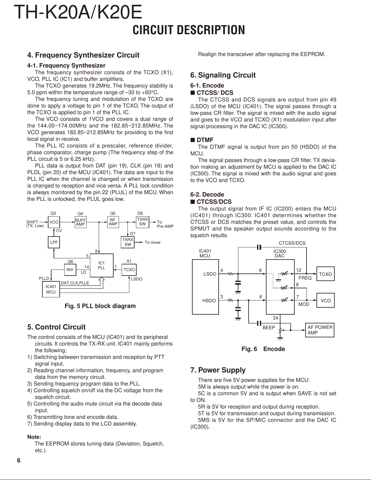
4. Frequency Synthesizer Circuit
4-1. Frequency Synthesizer
The frequency synthesizer consists of the TCXO (X1),
VCO, PLL IC (IC1) and buffer amplifi ers.
The TCXO generates 19.2MHz. The frequency stability is
5.0 ppm within the temperature range of –30 to +60°C.
The frequency tuning and modulation of the TCXO are
done to apply a voltage to pin 1 of the TCXO. The output of
the TCXO is applied to pin 1 of the PLL IC.
The VCO consists of 1VCO and covers a dual range of
the 144.00~174.00MHz and the 182.85~212.85MHz. The
VCO generates 182.85~212.85MHz for providing to the fi rst
local signal in receive.
The PLL IC consists of a prescaler, reference divider,
phase comparator, charge pump (The frequency step of the
PLL circuit is 5 or 6.25 kHz).
PLL data is output from DAT (pin 19), CLK (pin 18) and
PLDL (pin 20) of the MCU (IC401). The data are input to the
PLL IC when the channel is changed or when transmission
is changed to reception and vice versa. A PLL lock condition
is always monitored by the pin 22 (PLUL) of the MCU. When
the PLL is unlocked, the PLUL goes low.
SHIFT
(TX: Low)
PLLD
Q3
VCO
LPF
IC401
MCU
Q4
BUFF
AMP
CV
Q6
INV
DAT,CLK,PLLE
5
14
LD
Fig. 5 PLL block diagram
Q5
RF
AMP
8
IC1
1
PLL
TXRX
SW
X1
TCXO
D7
LSDO
D8
TXRX
SW
To mixer
To
Pre-AMP
Realign the transceiver after replacing the EEPROM.
6. Signaling Circuit
6-1. Encode
CTCSS/ DCS
■
The CTCSS and DCS signals are output from pin 49
(LSDO) of the MCU (IC401). The signal passes through a
low-pass CR fi lter. The signal is mixed with the audio signal
and goes to the VCO and TCXO (X1) modulation input after
signal processing in the DAC IC (IC300).
DTMF
■
The DTMF signal is output from pin 50 (HSDO) of the
MCU.
The signal passes through a low-pass CR fi lter. TX devia-
tion making an adjustment by MCU is applied to the DAC IC
(IC300). The signal is mixed with the audio signal and goes
to the VCO and TCXO.
6-2. Decode
CTCSS/DCS
■
The output signal from IF IC (IC200) enters the MCU
(IC401) through IC300. IC401 determines whether the
CTCSS or DCS matches the preset value, and controls the
SPMUT and the speaker output sounds according to the
squelch results.
CTCSS/DCS
IC401
MCU
LSDO
HSDO
4
3
IC300
DAC
9
6
12
FREQ
8
7
MOD
TCXO
VCO
5. Control Circuit
The control consists of the MCU (IC401) and its peripheral
circuits. It controls the TX-RX unit. IC401 mainly performs
the following;
1) Switching between transmission and reception by PTT
signal input.
2) Reading channel information, frequency, and program
data from the memory circuit.
3) Sending frequency program data to the PLL.
4) Controlling squelch on/off via the DC voltage from the
squelch circuit.
5) Controlling the audio mute circuit via the decode data
input.
6) Transmitting tone and encode data.
7) Sending display data to the LCD assembly.
Note:
The EEPROM stores tuning data (Deviation, Squelch,
etc.).
6
24
BEEP
AF POWER
AMP
Fig. 6 Encode
7. Power Supply
There are fi ve 5V power supplies for the MCU:
5M is always output while the power is on.
5C is a common 5V and is output when SAVE is not set
to ON.
5R is 5V for reception and output during reception.
5T is 5V for transmission and output during transmission.
5MS is 5V for the SP/MIC connector and the DAC IC
(IC300).

TH-K20A/K20E
SEMICONDUCTOR DATA
MCU: R5F2L3ACCKEKA (TX-RX unit IC401
Pin No. Port Name I/O Function
1 KEYIT I Type detection
2 KEYIS I Type detection
3 HSDO O DTMF/BEEP/1750Hz tone output
4 LSDO O CTCSS/DCS tone output
5 WKUPO - Ground
6 VREF - Reference voltage input
7 MODE - MCU mode select
8 XCIN - Not used (Pull-up)
9 XCOUT - Not used
10 RESET I MCU reset
11 XOUT O 11.0592MHz MCU clock output
12 VSS - Ground
13 XIN I 11.0592MHz clock input for MCU
14 VCC - 5V power supply (5M)
15 BSFT O Beat shift control
16 INPTT I
17 5RC O
18,19 ENC2-ENC1 I Encoder input 2,1
20 RxD I Serial data input from PC
21 TxD O Serial data input to PC
22 W/N O
23 PLLE O
24 PLPS O
25 PLLD I
26 EXPTT I
27 LAMP O
28 NC O Not used
29 E2PCS O
30 E2PIN I Data input from EEPROM
31-34 COM0-COM3 O
35-66 SEG0-SEG31 O
67 LEDR O
68 LEDG O
69 5VC O
70 5MSC O
71 SPM O
INT PTT switch input
L: Active
5R RX power switch control
L: Active
Wide/Narrow control
H: Narrow
PLL-IC enable
H: Active
PLL-IC save control
L: Save ON
PLL unlock detect
L: Unlock
EXT-PTT input
L: Active
BacKlight LED control
H: Lights
EEPROM chip select
L: Active
LCD common output
H: Active
LCD segment output
H: Active
TX LED (Red) control
H: Lights
BUSY LED (Green) control
H: Lights
5V MIC AMP power switch control
L: Active
5MS main power switch control
L: Active
Speaker mute control
L: Mute
)
Pin No. Port Name I/O Function
72 MONI I
73 CLK O Common serial clock output
74 DATA O Common serial data output
75 5CC O
76 5TC O
77 VOLCS O
78 VDCSW O
79 CURRENT I TX current detect
80 VOX I VOX level detect
81 REM I
82 BATT I Battery voltage detection
83 THERM I Temperture detect
84 RSSI I RSSI level detect
85 SQL I Squelch level detect
86 LSDI I CTCSS/DCS tone detect
87 CVDET I VCO controle voltage detect
88-90
91-93 VL1-VL3 - LCD drive power supply
94 SHIFT O
95 KEYO1 O Key matrix output 1
96 VL4 - LCD drive power supply
97-100 KEYI1-KEYI4 I Key matrix input 1-4
KEYO4-
KEYO2
[MONI] key switch input
L: Active
5C Common power switch control
L: Active
5T TX power switch control
L: Active
DAC-IC chip select
L: Active
Voltage discharge control
H: Active
Remote control microphone key
detect
O Key matrix output 4-2
VCO TX/RX control
H: TX
7

TH-K20A/K20E
SEMICONDUCTOR DATA
PLL IC: MB15E03SL-E1 (TX-RX unit IC1)
Pin No. Port Name I/O Function
1 OSCIN I
2 OSCOUT O Oscillator output
3VP -
4 VCC - Power supply voltage (3.0V)
5 DO O Charge pump output
6 GND - Ground
7 XFIN I
8 FIN I Prescaler input
9 ClOCK I
1 0 D ATA I
11 LE I Load enable signal input
12 PS I
13 ZC I
14 LD/FOUT O Lock detect signal output
15
16
PO
RO
Programmable reference divider
input
Power supply voltage input for the
charge pump
Prescaler complementary input
which should be grounded via a
capacitor
Clock input for the 19-bit shift reg-
ister
Serial data input using binary
code
Power saving mode control
This pin must be set at “L” at
Power-ON.
Forced high-impedance control
for the charge pump
Phase comparator N-channel
open drain output for an external
charge pump (Not use)
Phase comparator CMOS output
for an external charge pump (Not
use)
FM IC: TA31136FNG (TX-RX unit IC200)
Pin No. Port Name I/O Function
1 OSCIN I 2nd Local oscillator input
2 OSCOUT O 2nd Local oscillator output
3 MIXOUT O MIX output
4 VCC - Power supply (5.0V)
5 IFIN I 2nd IF input and decoupling
6 DEC - 2nd IF input and decoupling
7 FILOUT O INVERTER AMP output
8 FILIN I INVERTER AMP input
9 AFOUT O Demodulate signal output
10 QUAD I
11 IFOUT O Output terminal of IF AMP
12 RSSI O This terminal outputs DC
13 NOISEDET - level according to input (Not use)
14 NOISEREC - signal level to IF AMP
15 GND - Ground
16 MIXIN I 1st IF signal input
Phase shift signal input of FM
demodulator
D/A Converter IC: R2A20178NP (TX-RX unit IC300)
Pin No. Port Name I/O Function
1 Vin2 I FROM AF fi lter signal input
2 VDD - Power supply voltage (5.0V)
3 LD I Load enable signal input
4 CLK I Control data input
5 DI I Control clock input
6 Vin3 I
7 Vout3 O Load enable signal input
8 Vout4 O Tone deviation adjust
9 Vin4 I Tone signal input
10 Vin5 I Connect to ground
11 Vout5 O VCO assist voltage adjust
12 Vout6 O TCXO frequency adjust
13 Vin6 I Connect to ground
14 VDAREF1 -
15 VDAREF2 -
16 /RESET I Reset
17 GND - Ground
18 Vin7 I Connect to ground
19 Vout7 O RX BPF tuning adjust
20 Vout8 O TX power adjust
21 Vin8 I Connect to ground
22 Vin1 I From MIC output
23 Vout1 O MIC level contorol and mute
24 Vout2 O RX AF mute control
From MIC AMP and limiter signal
input
Reference voltage 1 for DAC
(1.8V)
Reference voltage 1 for DAC
(5.0V)
8

TH-K20A/K20E
COMPONENTS DESCRIPTION
TX-RX unit (X57-821X-XX)
Ref. No. Use/Function
IC1 PLL system Frequency control
IC200 FM IF system
IC300 D/A converter
IC301 OP AMP
IC302 OP AMP Detect AF fi lter
IC303 OP AMP CTCSS/DCS fi lter
IC304 OP AMP MIC amolifi er/IDC
IC305
IC306
IC307
IC308
IC400 EEPROM Tuning data/Memory data
IC401 MCU
Q1
Q2 Ripple fi lter for VCO power supply
Q3 Oscillator TX/RX VCO
Q4 Buffer amplifi er for VCO output
Q5 RF amplifi er for VCO output
Q6 Logic invert for unlock signal
Q7
Q101
Q102 Drive amplifi er
Q103 Final amplifi er 5.5W RF power
Q104
Q200
Q201 Doubler 2nd Lo: 38.4MHz
Q202 1st IF amplifi er 1st IF: 38.85MHz
Q203 1st mixer
Q204 RF amplifi er RX 1st amplifi re
Q300
Q301
Q302
Q303
Voltage
detector/3.3V
Voltage
regulator/5.0V
AF power ampli-
fi e r
Voltage
regulator/5.0V
VCO shift control
switch
Power supply
(3.0V)
Pre drive amplifi er
Voltage dis-
charge switch
Wide/Narrow
switch
Power supply
(5.0V) switch
SP mute control
switch
SP mute control
switch
Speaker mute
switch
Operation/Condition/Compatibility
2nd mixer, IF amplifi er, FM
detector
AF mute/MOD level and fre-
quency adjust
1.8V reference voltage/MIC
amolifi er
MCU reset
5M/5MS power supply
Speaker output
5C/5T/5R power supply
TX: ON
for PLL IC
for FET bias voltage.
Active ON (VDCSW: H)
for ceramic fi lter selector
Wide: ON (W/L: L)
Active ON (5VC: L)
Active ON (SM: H)
for pop-noise Active ON
for AF signal line Active ON
Ref. No. Use/Function
Q304
Q305
Q306
Q307
Q308
Q400 Beat shift switch Active ON (BSFT: H)
Q401
Q402
Q403 Busy LED switch Active ON (LEDG: H)
Q404 TX LED switch Active ON (LEDR: H)
D1,D2
D3 RF switch
D4 VCO modulation for frequency modulation
D5
D6 Speed up for ripple fi lter
D7 RF switch for TX signal TX: ON
D8 RF switch for RX signal
D9, D10 Speed up for ripple fi lter
D11 Speed up for VCO shift control line
D101-104 Antenna switch TX: ON
D200, D201
D203
D300 VOX signal detect
D301
D302
D304
D401
D404-411
D414, D415
D416-425
D426 Busy LED Busy: light
D427 TX LED TX: light
Power supply
(5MS) switch
Speaker mute
switch
IC power supply
switch
Power supply
(5R) switch
Power supply
(5T) switch
Backlight LED
switch
Backlight control
switch
VCO frequency
control
Assist frequency
control
Band-pass fi lter
tuning
Band-pass fi lter
tuning
Reverse connec-
tion protection
Reverse current
prevention
Reverse current
prevention
Over voltage limit-
ter
Reverse current
prevention
LCD backlight
LED
Key backlight
LED
Operation/Condition/Compatibility
Active ON (5MSC: L)
for AF signal line Active ON
for AF power IC Active ON
Active ON (5RC: L)
Active ON (5TC: L)
Active ON
Active ON (LAMP: H)
for frequency range change
TX: ON
VHF band for receiver
VHF band for receiver
Battry terminal
for IC306 input
for IC308 input
3.6V zener diode
Key matrix
9
TH-K20A/K20E
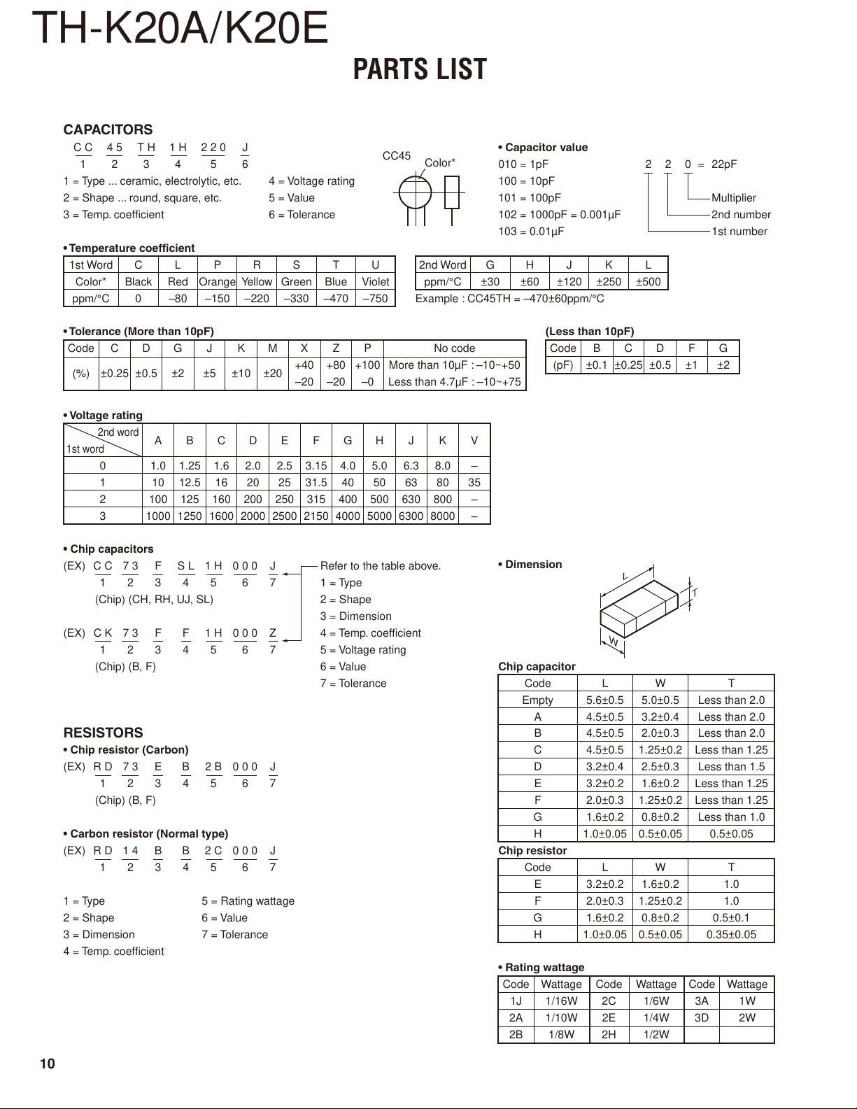
C C 4 5 T H 1 H 2 2 0 J
1 2 3 4 5 6
1 = Type ... ceramic, electrolytic, etc. 4 = Voltage rating
2 = Shape ... round, square, etc. 5 = Value
3 = Temp. coefficient 6 = Tolerance
1st Word C L P R S T U
Color* Black Red Orange Yellow Green Blue Violet
ppm/°C 0 –80 –150 –220 –330 –470 –750
PARTS LIST
CC45
Color*
2nd Word G H J K L
ppm/°C ±30 ±60 ±120 ±250 ±500
Example : CC45TH = –470±60ppm/°C
010 = 1pF 2 2 0 = 22pF
100 = 10pF
101 = 100pF Multiplier
102 = 1000pF = 0.001µF 2nd number
103 = 0.01µF 1st number
Code C D G J K M X Z P No code
(%) ±0.25 ±0.5 ±2 ±5 ±10 ±20
–20 –20 –0 Less than 4.7µF : –10~+75
2nd word
1st word
0 1.0 1.25 1.6 2.0 2.5 3.15 4.0 5.0 6.3 8.0 –
1 10 12.5 16 20 25 31.5 40 50 63 80 35
2 100 125 160 200 250 315 400 500 630 800 –
3 1000 1250 1600 2000 2500 2150 4000 5000 6300 8000 –
(EX) C C 7 3 F S L 1 H 0 0 0 J Refer to the table above.
1 2 3 4 5 6 7 1 = Type
(Chip) (CH, RH, UJ, SL) 2 = Shape
3 = Dimension
(EX) C K 7 3 F F 1 H 0 0 0 Z 4 = Temp. coefficient
1 2 3 4 5 6 7 5 = Voltage rating
(Chip) (B, F) 6 = Value
7 = Tolerance
A B C D E F G H J K V
(EX) R D 7 3 E B 2 B 0 0 0 J
1 2 3 4 5 6 7
(Chip) (B, F)
(EX) R D 1 4 B B 2 C 0 0 0 J
1 2 3 4 5 6 7
1 = Type 5 = Rating wattage
2 = Shape 6 = Value
3 = Dimension 7 = Tolerance
4 = Temp. coefficient
+40 +80 +100 More than 10µF : –10~+50
Chip capacitor
Code L W T
Empty 5.6±0.5 5.0±0.5 Less than 2.0
A 4.5±0.5 3.2±0.4 Less than 2.0
B 4.5±0.5 2.0±0.3 Less than 2.0
C 4.5±0.5 1.25±0.2 Less than 1.25
D 3.2±0.4 2.5±0.3 Less than 1.5
E 3.2±0.2 1.6±0.2 Less than 1.25
F 2.0±0.3 1.25±0.2 Less than 1.25
G 1.6±0.2 0.8±0.2 Less than 1.0
H 1.0±0.05 0.5±0.05 0.5±0.05
Chip resistor
Code L W T
E 3.2±0.2 1.6±0.2 1.0
F 2.0±0.3 1.25±0.2 1.0
G 1.6±0.2 0.8±0.2 0.5±0.1
H 1.0±0.05 0.5±0.05 0.35±0.05
Code Wattage Code Wattage Code Wattage
1J 1/16W 2C 1/6W 3A 1W
2A 1/10W 2E 1/4W 3D 2W
2B 1/8W 2H 1/2W
Code B C D F G
(pF) ±0.1 ±0.25 ±0.5 ±1 ±2
L
T
W
10

PARTS LIST
TH-K20A/K20E
New Parts.
✽
Parts without Parts No. are not supplied.
Les articles non mentionnes dans le Parts No. ne sont pas fournis.
Teile ohne Parts No. werden nicht geliefert.
Ref. No.
indicates safety critical components.
New
Address
Parts No. Description
parts
TH-K20A/K20E TX-RX UNIT (X57-821X-XX) 0-11: K 0-20: M 2-71: E
1 1A ✽ A02-4158-03 PLASTIC CABINET ASSY
2 3A
3 3B
4 3B
6 1A
7 2B B11-1892-03 ILLUMINATION GUIDE (TX/BUSY)
8 1A
9 1D
11 1D
12 1D
13 1D
14 1D
15 1D
16 1D
18 1D
19 2B
21 2A
23 1B
24 2A
26 3B G01-4571-04 COIL SPRING
27 2A G11-4437-04 SHEET (Q103-CHASSIS)
29 3B
31 3A G13-2368-04 CUSHION (BATTERY)
32 2A G53-1867-13 PACKING (CHASSIS)
33 2B
34 2A
36 3B
37 2D
38 1C
41 3D
42 2C J29-0756-05 BELT CLIP ACCESSORY
46 3A K29-9491-03 LEVER KNOB
47 1A
48 1B
49 1B
51 1A
52 1A
A 2B N09-2438-05 BINDING HEAD SCREW (ANT)
B 3A N80-2608-43 PAN HEAD TAPTITE SCREW
C
54 1B T07-0787-05 SPEAKER
56 2C T90-1018-35
57 2C T90-1044-15
58 1C W08-1246-15 AC ADAPTER ACCESSORY M,E
59 1C W08-1247-15 AC ADAPTER ACCESSORY K
61 2D
62 1C W09-1073-25 BATTERY ASSY ACCESSORY
A10-4158-01 CHASSIS
✽
A82-0085-02 REAR PANEL
✽
B09-0749-03 CAP (EXT SP/MIC)
✽
B10-6009-03 FRONT GLASS
✽
B11-1897-02 ILLUMINATION GUIDE (16KEY)
✽
B62-2365-00
✽
B62-2369-00
✽
B62-2370-00
✽
B62-2371-00
✽
B62-2372-00
✽
B62-2373-00
✽
B62-2374-00
✽
B62-2375-00
✽
E04-0488-05
✽
E23-1373-04 TERMINAL
✽
E37-1543-05
✽
E72-0437-03 TERMINAL BLOCK
✽
G13-2366-04 CUSHION (TERMINAL)
✽
G53-1880-02 PACKING (TOP)
✽
G53-1881-04 PACKING (ECM)
✽
G53-1882-03 PACKING (SP/MIC)
✽
H12-4324-02 PACKING FIXTURE K
✽
H12-4326-02 PACKING FIXTURE K
✽
H52-2486-02 ITEM CARTON CASE K
✽
K29-9502-02 KEY TOP
✽
K29-9503-03 KNOB (VOL/PSW)
✽
K29-9504-03 KNOB (ENCODER)
✽
K29-9505-03 KNOB (PTT)
✽
K29-9506-03 BUTTON KNOB (SIDE)
✽
1A,2A,2B
N83-2005-48 PAN HEAD TAPTITE SCREW
W08-1249-35 CHARGER ACCESSORY
✽
X57-8210-12 TX-RX UNIT (FOR SERVICE) K
✽
X57-8210-21 TX-RX UNIT (FOR SERVICE) M
✽
X57-8212-72 TX-RX UNIT (FOR SERVICE) E
✽
INSTRUCTION MANUAL ACCESSORY
INSTRUCTION MANUAL ACCESSORY
INSTRUCTION MANUAL ACCESSORY
INSTRUCTION MANUAL ACCESSORY
INSTRUCTION MANUAL ACCESSORY
INSTRUCTION MANUAL ACCESSORY
INSTRUCTION MANUAL ACCESSORY
INSTRUCTION MANUAL ACCESSORY
RF COAXIAL RECEPTACLE (SMA)
LEAD WIRE WITH CONNECTOR (SP)
HELICAL ANTENNA ACCESSORY
HELICAL ANTENNA ACCESSORY
(X57)
K,E
K,E
E
E
E
E
M
M
K,E
Desti-
nation
L : Scandinavia K : USA P : Canada
Y : PX (Far East, Hawaii) T : England E : Europe
C : China X : Australia M : Other Areas
TX-RX UNIT (X57-821X-XX)
Ref. No.
101 3A
102 3A
D414,415 B30-2261-05 LED (YELLOW/LCD)
D416-425 B30-2337-05 LED (YELLOW/KEY))
D426 B30-1782-05 LED (GREEN/BUSY)
D427 B30-1779-05 LED (RED/TX)
103 2A
C1 CK73HB1A184K CHIP C 0.18UF K
C2 CK73HB1C333K CHIP C 0.033UF K
C3 CK73HB1A105K CHIP C 1.0UF K
C4 CK73HB1E223K CHIP C 0.022UF K
C5 CC73HCH1H390G CHIP C 39PF G
C6 CK73HB1E223K CHIP C 0.022UF K
C7 CC73HCH1H0R5B CHIP C 0.5PF B
C8 CK73HB1H102K CHIP C 1000PF K
C9 CK73HB1A105K CHIP C 1.0UF K
C10 CC73HCH1H080B CHIP C 8.0PF B
C11 CK73HB1H102K CHIP C 1000PF K
C12 CS77CP0J010M CHIP TNTL 1.0UF 6.3WV
C13 CK73HB1H102K CHIP C 1000PF K
C15 CC73HCH1H100B CHIP C 10PF B
C16 CS77CA1A220M CHIP TNTL 22UF 10WV
C17 CC73HCH1H090B CHIP C 9.0PF B
C18 CK73HB1H102K CHIP C 1000PF K
C19 CK73HB1E103K CHIP C 0.010UF K
C20 ,21 CK73HB1H102K CHIP C 1000PF K
C22 CC73GCH1H0R5B CHIP C 0.5PF B
C23 CK73HB1H102K CHIP C 1000PF K
C25 CK73HB1H102K CHIP C 1000PF K
C26 CC73HCH1H150J CHIP C 15PF J
C27 CC73HCH1H470G CHIP C 47PF G
C28 CC73HCH1H090B CHIP C 9.0PF B
C29 CC73HCH1H150J CHIP C 15PF J
C31 CC73HCH1H120J CHIP C 12PF J
C32 ,33 CK73HB1H102K CHIP C 1000PF K
C34 CC73HCH1H150J CHIP C 15PF J
C36 CK73HB1H102K CHIP C 1000PF K
C37 CK73GB1E154K CHIP C 0.15UF K
C38 CS77CA1A6R8M CHIP TNTL 6.8UF 10WV
C39 CS77CA1DR68M CHIP TNTL 0.68UF 20WV
C41 CK73HB1E103K CHIP C 0.010UF K
C42 CK73HB1H102K CHIP C 1000PF K
C43 CK73HB1E103K CHIP C 0.010UF K
C44 CK73HB1H102K CHIP C 1000PF K
C45 CC73HCH1H220J CHIP C 22PF J
C46 CK73HB1H102K CHIP C 1000PF K
C47 CC73HCH1H040B CHIP C 4.0PF B
C48 CK73HB1E103K CHIP C 0.010UF K
C49 CK73HB1H102K CHIP C 1000PF K
C50 CC73HCH1H050C CHIP C 5.0PF C
C51 CC73GCH1H220J CHIP C 22PF J
C101 CC73HCH1H220J CHIP C 22PF J
C102 CK73HB1H102K CHIP C 1000PF K
Address
New
Parts No. Description
parts
B11-1895-03 ILLUMINATION GUIDE (LCD)
✽
B11-1896-04 FILTER (LCD)
✽
B38-0939-05 LCD
✽
TH-K20A/K20E
Desti-
nation
M: TH-K20A(M)
K : TH-K20A(K)
E : TH-K20E(E)
11
TH-K20A/K20E
TX-RX UNIT (X57-821X-XX)
Ref. No.
C104,105 CK73HB1H102K CHIP C 1000PF K
C106 CC73HCH1H090B CHIP C 9.0PF B
C107 CK73HB1H102K CHIP C 1000PF K
C108 CC73HCH1H150J CHIP C 15PF J
C109 CK73HB1H102K CHIP C 1000PF K
Address
New
Parts No. Description
parts
PARTS LIST
Desti-
nation
Ref. No.
C234 CK73HB1E103K CHIP C 0.010UF K
C235 CK73HB1H102K CHIP C 1000PF K
C237 CC73HCH1H220J CHIP C 22PF J
C239,240 CK73HB1H102K CHIP C 1000PF K
C244 CK73HB1H102K CHIP C 1000PF K
Address
New
Parts No. Description
parts
Desti-
nation
C110 CK73HB1A104K CHIP C 0.10UF K
C112 CK73HB1E103K CHIP C 0.010UF K
C113 CC73HCH1H560J CHIP C 56PF J
C115 CK73HB1H102K CHIP C 1000PF K
C125 CC73GCH1H390J CHIP C 39PF J
C127 CC73GCH1H470J CHIP C 47PF J
C129 CC73GCH1H150J CHIP C 15PF J
C133 CC73GCH1H270J CHIP C 27PF J
C134 CK73GB1H102K CHIP C 1000PF K
C135 CC73GCH1H060B CHIP C 6.0PF B
C136 CK73GB1H102K CHIP C 1000PF K
C137 CC73GCH1H120J CHIP C 12PF J
C138 CC73GCH1H060B CHIP C 6.0PF B
C139 CC73GCH1H270J CHIP C 27PF J
C140 CC73GCH1H060B CHIP C 6.0PF B
C141 CC73GCH1H120J CHIP C 12PF J
C144 CC73GCH1H220J CHIP C 22PF J
C146 CC73HCH1H180J CHIP C 18PF J
C147 CK73HB1A105K CHIP C 1.0UF K
C148 CK73HB1H102K CHIP C 1000PF K
C150 CK73HB1H102K CHIP C 1000PF K
C151 CK73FB1A225K CHIP C 2.2UF K
C152-157 CK73HB1H102K CHIP C 1000PF K
C159 CK73FB1A225K CHIP C 2.2UF K
C160 CK73HB1H102K CHIP C 1000PF K
C161 CK73HB1E103K CHIP C 0.010UF K
C162 CK73HB1H102K CHIP C 1000PF K
C200 CK73FB1A106K CHIP C 10UF K
C201 CK73HB1H102K CHIP C 1000PF K
C202 CK73HB1E103K CHIP C 0.010UF K
C245 CC73HCH1H020B CHIP C 2.0PF B
C246 CC73HCH1H390G CHIP C 39PF G
C247 CK73HB1H102K CHIP C 1000PF K
C248 CC73HCH1H010B CHIP C 1.0PF B
C249 CC73HCH1H390G CHIP C 39PF G
C250 CC73HCH1H020B CHIP C 2.0PF B
C251 CK73HB1H102K CHIP C 1000PF K
C253-255 CK73HB1H102K CHIP C 1000PF K
C256 CC73HCH1H470G CHIP C 47PF G
C259 CK73HB1H102K CHIP C 1000PF K
C261 CC73HCH1H390G CHIP C 39PF G
C265 CC73HCH1H470G CHIP C 47PF G
C266 CC73HCH1H030B CHIP C 3.0PF B
C270 CC73HCH1H010B CHIP C 1.0PF B
C271 CC73HCH1H390G CHIP C 39PF G
C272 CC73HCH1H030B CHIP C 3.0PF B
C273 CC73HCH1H010B CHIP C 1.0PF B
C301,302 CK73HB1A104K CHIP C 0.10UF K
C304 CK73HB1C473K CHIP C 0.047UF K
C305,306 CK73HB1A105K CHIP C 1.0UF K
C307 CK73HB1A224K CHIP C 0.22UF K
C308 CK73HB1A104K CHIP C 0.10UF K
C310 CK73HB1A104K CHIP C 0.10UF K
C311 CK73HB1C273K CHIP C 0.027UF K
C312 CK73HB1H472K CHIP C 4700PF K
C313 CK73HB1A104K CHIP C 0.10UF K
C314 CK73HB1E103K CHIP C 0.010UF K
C316 CK73HB1A184K CHIP C 0.18UF K
C317 CK73HB1A104K CHIP C 0.10UF K
C318-321 CK73HB1A184K CHIP C 0.18UF K
C203 CC73HCH1H271J CHIP C 270PF J
C204 CK73HB1H182K CHIP C 1800PF K
C205 CK73HB1A104K CHIP C 0.10UF K
C206,207 CC73HCH1H271J CHIP C 270PF J
C208 CK73HB1A104K CHIP C 0.10UF K
C209 CC73HCH1H470G CHIP C 47PF G
C211 CK73HB1A104K CHIP C 0.10UF K
C212 CK73HB1C333K CHIP C 0.033UF K
C213,214 CK73HB1A104K CHIP C 0.10UF K
C215 CK73HB1E103K CHIP C 0.010UF K
C216 CC73HCH1H220J CHIP C 22PF J
C217 CK73HB1E103K CHIP C 0.010UF K
C218 CC73HCH1H050C CHIP C 5.0PF C
C219 CC73HCH1H220J CHIP C 22PF J
C220 CK73HB1H102K CHIP C 1000PF K
C221 CK73HB1E103K CHIP C 0.010UF K
C223 CK73HB1E103K CHIP C 0.010UF K
C226 CC73HCH1H080B CHIP C 8.0PF B
C227 CC73HCH1H060B CHIP C 6.0PF B
C228 CK73HB1E103K CHIP C 0.010UF K
C229 CC73HCH1H050C CHIP C 5.0PF C
C230 CC73HCH1H100B CHIP C 10PF B
C231 CC73HCH1H050C CHIP C 5.0PF C
C232 CC73HCH1H101J CHIP C 100PF J
C233 CK73HB1H102K CHIP C 1000PF K
12
C322 CK73HB1A394K CHIP C 0.39UF K
C323 CK73HB1H332K CHIP C 3300PF K
C324 CK73HB1A184K CHIP C 0.18UF K
C325 CK73HB1A104K CHIP C 0.10UF K
C326 CC73HCH1H181J CHIP C 180PF J
C327 CK73HB1H472K CHIP C 4700PF K
C328 CK73HB1E103K CHIP C 0.010UF K
C329 CK73GB1C225K CHIP C 2.2UF K
C330,331 CC73HCH1H271J CHIP C 270PF J
C332 CK73HB1A105K CHIP C 1.0UF K
C333 CK73HB1H822K CHIP C 8200PF K
C334 CK73HB1C273K CHIP C 0.027UF K
C335 CC73HCH1H271J CHIP C 270PF J
C336 CK73HB1H821K CHIP C 820PF K
C337 CK73HB1E103K CHIP C 0.010UF K
C338 CK73HB1H102K CHIP C 1000PF K
C339 CC73HCH1H100B CHIP C 10PF B
C340,341 CK73HB1E103K CHIP C 0.010UF K
C342 CK73HB1H102K CHIP C 1000PF K
C344 CC73HCH1H271J CHIP C 270PF J
C345 CC73HCH1H101J CHIP C 100PF J
C347 CK73HB1H102K CHIP C 1000PF K
C351,352 CK73HB1H102K CHIP C 1000PF K
C353 CK73HB1C473K CHIP C 0.047UF K
C354 CK73HB1H102K CHIP C 1000PF K
M: TH-K20A(M)
K : TH-K20A(K)
E : TH-K20E(E)

PARTS LIST
Ref. No.
C356 CK73FB1A106K CHIP C 10UF K
C357 C92-0953-05 ELECTRO 100UF 6.3WV
C358 CK73FB1A475K CHIP C 4.7UF K
C359 CK73HB1E103K CHIP C 0.010UF K
C360,361 CK73HB1A224K CHIP C 0.22UF K
Address
New
Parts No. Description
parts
Desti-
nation
TH-K20A/K20E
TX-RX UNIT (X57-821X-XX)
Ref. No.
L10 L40-2775-71 SMALL FIXED INDUCTOR (27NH)
L11 L40-8275-71 SMALL FIXED INDUCTOR (82NH)
L13 L40-4763-92 SMALL FIXED INDUCTOR
L101 L40-6875-71 SMALL FIXED INDUCTOR (68NH)
L103 L40-1085-71 SMALL FIXED INDUCTOR
Address
New
Parts No. Description
parts
(4.7NH)
(100NH)
Desti-
nation
C363 CK73HB1H102K CHIP C 1000PF K
C364 CK73HB1A105K CHIP C 1.0UF K
C365 CK73HB1H102K CHIP C 1000PF K
C366 CK73FB1A106K CHIP C 10UF K
C367 CK73GB1E105K CHIP C 1.0UF K
C369 CK73HB1C473K CHIP C 0.047UF K
C371 CK73HB1C273K CHIP C 0.027UF K
C372 CK73FB1A106K CHIP C 10UF K
C373 CC73HCH1H101J CHIP C 100PF J
C374 CK73HB1A563K CHIP C 0.056UF K
C375 CK73GB1E105K CHIP C 1.0UF K
C376 CK73FB1A475K CHIP C 4.7UF K
C377 CK73GB1E105K CHIP C 1.0UF K
C379 CC73HCH1H221J CHIP C 220PF J
C380 CK73HB1H102K CHIP C 1000PF K
C381 CK73HB1A104K CHIP C 0.10UF K
C382 CC73HCH1H271J CHIP C 270PF J
C383-385 CK73HB1H102K CHIP C 1000PF K
C386 CK73HB1C473K CHIP C 0.047UF K
C402 CK73HB1H102K CHIP C 1000PF K
C404-407 CK73FB0J226M CHIP C 22UF M
C411 CC73HCH1H120J CHIP C 12PF J
C412 CC73HCH1H010B CHIP C 1.0PF B
C413 CK73HB1A104K CHIP C 0.10UF K
C414 CK73HB1H102K CHIP C 1000PF K
C415 CC73HCH1H120J CHIP C 12PF J
C417,418 CK73HB1H102K CHIP C 1000PF K
C419 C93-1803-05 CHIP C 10UF M
C420,421 CK73HB1H102K CHIP C 1000PF K
C423 CK73HB1H102K CHIP C 1000PF K
C424,425 CK73HB1E103K CHIP C 0.010UF K
C427 CK73HB1H102K CHIP C 1000PF K
C428 CK73HB1E103K CHIP C 0.010UF K
J300 2B E11-0484-05 3.5D PHONE JACK (3.5D/MIC)
J301 2B E11-0717-05 2.5D PHONE JACK (2.5D/SP)
104 3A
CN300 E40-6900-05 PIN ASSY (INT SP)
F101 F53-0287-05 FUSE (0.5A)
F300 F53-0372-05 FUSE (3.15A)
F301 F53-0467-05 FUSE (0.315A)
105 2A
106 2A
107 2A J30-1267-04 SPACER (ECM)
CD200 L79-1474-05 TUNING COIL (450KHZ)
CF200 L72-1042-05 CERAMIC FILTER (450KHZ)
L1 L40-2285-92 SMALL FIXED INDUCTOR
L2 L40-1885-92 SMALL FIXED INDUCTOR
L3 L40-1001-86 SMALL FIXED INDUCTOR (10UH)
L4 L41-2778-08 SMALL FIXED INDUCTOR (27NH)
L5 L41-2278-08 SMALL FIXED INDUCTOR (22NH)
L6 L40-1001-86 SMALL FIXED INDUCTOR (10UH)
L8 L40-1001-86 SMALL FIXED INDUCTOR (10UH)
L9 L40-1285-71 SMALL FIXED INDUCTOR
M: TH-K20A(M)
K : TH-K20A(K)
E : TH-K20E(E)
E29-1235-04 INTER CONNECTOR (LCD)
✽
G11-4563-04 SHEET (LCD)
✽
J21-8639-03 MOUNTING HARDWARE (LCD)
✽
(220NH)
(180NH)
(120NH)
If a part reference number is listed in a shaded box, that part does not come with the PCB.
L104 L40-3375-71 SMALL FIXED INDUCTOR (33NH)
L105 L41-8275-53 SMALL FIXED INDUCTOR (82NH)
L106 L34-4577-05 AIR-CORE COIL (9T)
L107 L34-4574-05 AIR-CORE COIL (6T)
L108 L41-2295-52 SMALL FIXED INDUCTOR
L109,110 L34-4577-05 AIR-CORE COIL (9T)
L112 L34-4577-05 AIR-CORE COIL (9T)
L113 L34-4571-05 AIR-CORE COIL (3T)
L114 L34-4573-05 AIR-CORE COIL (5T)
L115 L34-4574-05 AIR-CORE COIL (6T)
L200,201 L40-5681-86 SMALL FIXED INDUCTOR
L202 L40-8281-86 SMALL FIXED INDUCTOR
L204 L40-2275-71 SMALL FIXED INDUCTOR (22NH)
L205 L40-1285-71 SMALL FIXED INDUCTOR
L206 L41-8285-14 SMALL FIXED INDUCTOR
L209 L41-8278-14 SMALL FIXED INDUCTOR (82NH)
L211 L41-8278-14 SMALL FIXED INDUCTOR (82NH)
L213 L41-6878-14 SMALL FIXED INDUCTOR (68NH)
L214 L41-1878-14 SMALL FIXED INDUCTOR (18NH)
L215 L40-2763-71 SMALL FIXED INDUCTOR
L217 L41-8278-14 SMALL FIXED INDUCTOR (82NH)
X1 L77-3074-05 TCXO (19.2 MHZ)
X400 L77-2974-05 CRYSTAL RESONATOR
XF200 L71-0669-05 MCF (38.85MHZ)
VR300 2B R31-0684-05 VARIABLE RESISTOR
CP1 RK74HB1J102J CHIP-COM 1.0K J 1/16W
R2 RK73HB1J272J CHIP R 2.7K J 1/16W
R3 RK73HB1J102J CHIP R 1.0K J 1/16W
R4 RK73HB1J153J CHIP R 15K J 1/16W
R5 RK73HB1J102J CHIP R 1.0K J 1/16W
R6 ,7 RK73HB1J104J CHIP R 100K J 1/16W
R8 RK73HB1J103J CHIP R 10K J 1/16W
R9 RK73HB1J104J CHIP R 100K J 1/16W
R10 RK73HB1J220J CHIP R 22 J 1/16W
R11 RK73HB1J472J CHIP R 4.7K J 1/16W
R12 RK73HB1J221J CHIP R 220 J 1/16W
R14 RK73HB1J102J CHIP R 1.0K J 1/16W
R15 RK73GB2A473J CHIP R 47K J 1/10W
R18 RK73GB2A000J CHIP R 0 J 1/10W
R19 RK73HB1J562J CHIP R 5.6K J 1/16W
R20 RK73HB1J332J CHIP R 3.3K J 1/16W
R21 RK73HB1J331J CHIP R 330 J 1/16W
R22 RK73HB1J332J CHIP R 3.3K J 1/16W
R23 RK73HB1J100J CHIP R 10 J 1/16W
R24 RK73HB1J332J CHIP R 3.3K J 1/16W
R25 RK73HB1J103J CHIP R 10K J 1/16W
R26 RK73HB1J472J CHIP R 4.7K J 1/16W
R27 RK73HB1J222J CHIP R 2.2K J 1/16W
R28 RK73HB1J821J CHIP R 820 J 1/16W
R30 -38 RK73HB1J103J CHIP R 10K J 1/16W
R39 RK73HB1J100J CHIP R 10 J 1/16W
R40 RK73HB1J560J CHIP R 56 J 1/16W
R41 RK73HB1J392J CHIP R 3.9K J 1/16W
R43 RK73HB1J100J CHIP R 10 J 1/16W
(2.2UH)
(0.56UH)
(0.82UH)
(120NH)
(820NH)
(2.7NH)
(11.0592MHZ)
(VOL/PSW)
13
TH-K20A/K20E
PARTS LIST
TX-RX UNIT (X57-821X-XX)
Ref. No.
R45 RK73HB1J333J CHIP R 33K J 1/16W
R46 RK73HB1J104J CHIP R 100K J 1/16W
R47 RK73GB2A105J CHIP R 1.0M J 1/10W
R48 RK73GB2A102J CHIP R 1.0K J 1/10W
R101 RK73HB1J180J CHIP R 18 J 1/16W
Address
New
Parts No. Description
parts
Desti-
nation
Ref. No.
R246 RK73HB1J104J CHIP R 100K J 1/16W
R247 RK73HB1J332J CHIP R 3.3K J 1/16W
R248 RK73HB1J152J CHIP R 1.5K J 1/16W
R249 RK73HB1J102J CHIP R 1.0K J 1/16W
R251 RK73HB1J105J CHIP R 1.0M J 1/16W
Address
New
Parts No. Description
parts
Desti-
nation
R102 RK73HB1J102J CHIP R 1.0K J 1/16W
R103 RK73HB1J222J CHIP R 2.2K J 1/16W
R104 RK73HB1J180J CHIP R 18 J 1/16W
R105 RK73HB1J331J CHIP R 330 J 1/16W
R107 RK73HB1J180J CHIP R 18 J 1/16W
R108 RK73HB1J100J CHIP R 10 J 1/16W
R109 RK73HB1J104J CHIP R 100K J 1/16W
R111 RK73HB1J823J CHIP R 82K J 1/16W
R112 RK73HB1J470J CHIP R 47 J 1/16W
R113 RK73HB1J683J CHIP R 68K J 1/16W
R114 RK73HB1J470J CHIP R 47 J 1/16W
R115 RK73HB1J563J CHIP R 56K J 1/16W
R116 RK73GB2A000J CHIP R 0 J 1/10W
R119 RK73GB2A000J CHIP R 0 J 1/10W
R120 RK73HB1J182J CHIP R 1.8K J 1/16W
R121 RK73HB1J393J CHIP R 39K J 1/16W
R124 RK73HB1J331J CHIP R 330 J 1/16W
R125 R92-3637-05 CHIP R 0.39 J 1/3W
R126 RK73HB1J271J CHIP R 270 J 1/16W
R127 R92-3637-05 CHIP R 0.39 J 1/3W
R128 RK73HB1J271J CHIP R 270 J 1/16W
R129 R92-3637-05 CHIP R 0.39 J 1/3W
R130 RK73FB2B000J CHIP R 0 J 1/8W
R200 RK73HB1J470J CHIP R 47 J 1/16W
R201 RK73HB1J152J CHIP R 1.5K J 1/16W
R203 RK73HB1J683J CHIP R 68K J 1/16W
R204 RK73HB1J332J CHIP R 3.3K J 1/16W
R205 RK73HB1J222J CHIP R 2.2K J 1/16W
R206 RK73HB1J334J CHIP R 330K J 1/16W
R207 RK73HB1J272J CHIP R 2.7K J 1/16W
R252,253 RK73HB1J472J CHIP R 4.7K J 1/16W
R300-302 RK73HB1J102J CHIP R 1.0K J 1/16W
R303-305 RK73HB1J103J CHIP R 10K J 1/16W
R307 RK73HB1J105J CHIP R 1.0M J 1/16W
R308 RK73HB1J102J CHIP R 1.0K J 1/16W
R309 RK73HB1J562J CHIP R 5.6K J 1/16W
R310 RK73HB1J393J CHIP R 39K J 1/16W
R311-313 RK73HH1J473D CHIP R 47K D 1/16W
R314 RK73HB1J824J CHIP R 820K J 1/16W
R315 RK73HB1J564J CHIP R 560K J 1/16W
R316 RK73HB1J103J CHIP R 10K J 1/16W
R317 RK73HB1J392J CHIP R 3.9K J 1/16W
R318 RK73HB1J272J CHIP R 2.7K J 1/16W
R319 RK73HB1J181J CHIP R 180 J 1/16W
R320 RK73HB1J563J CHIP R 56K J 1/16W
R321 RK73HB1J222J CHIP R 2.2K J 1/16W
R322 RK73HB1J332J CHIP R 3.3K J 1/16W
R323 RK73HB1J102J CHIP R 1.0K J 1/16W
R324 RK73HB1J561J CHIP R 560 J 1/16W
R325 RK73HB1J471J CHIP R 470 J 1/16W
R326 RK73HB1J562J CHIP R 5.6K J 1/16W
R327 RK73HB1J104J CHIP R 100K J 1/16W
R328 RK73HB1J103J CHIP R 10K J 1/16W
R329 RK73HB1J334J CHIP R 330K J 1/16W
R330 RK73HB1J104J CHIP R 100K J 1/16W
R331,332 RK73HH1J563D CHIP R 56K D 1/16W
R333,334 RK73HH1J473D CHIP R 47K D 1/16W
R335-338 RK73HB1J103J CHIP R 10K J 1/16W
R339,340 RK73HB1J102J CHIP R 1.0K J 1/16W
R341 RK73HB1J000J CHIP R 0 J 1/16W
R208 RK73HB1J183J CHIP R 18K J 1/16W
R210 RK73HB1J683J CHIP R 68K J 1/16W
R212 RK73HB1J101J CHIP R 100 J 1/16W
R213 RK73HB1J470J CHIP R 47 J 1/16W
R214 RK73HB1J334J CHIP R 330K J 1/16W
R215 RK73HB1J000J CHIP R 0 J 1/16W
R216 RK73HB1J184J CHIP R 180K J 1/16W
R218 RK73HB1J102J CHIP R 1.0K J 1/16W
R220 RK73HB1J681J CHIP R 680 J 1/16W
R221 RK73HB1J331J CHIP R 330 J 1/16W
R225 RK73HB1J470J CHIP R 47 J 1/16W
R226 RK73FB2B000J CHIP R 0 J 1/8W
R227 RK73HB1J331J CHIP R 330 J 1/16W
R228 RK73HB1J102J CHIP R 1.0K J 1/16W
R229-231 RK73HB1J823J CHIP R 82K J 1/16W
R232 RK73HB1J000J CHIP R 0 J 1/16W
R233,234 RK73HB1J105J CHIP R 1.0M J 1/16W
R235 RK73HB1J470J CHIP R 47 J 1/16W
R236 RK73HB1J820J CHIP R 82 J 1/16W
R237 RK73HB1J471J CHIP R 470 J 1/16W
R238 RK73HB1J104J CHIP R 100K J 1/16W
R239 RK73HB1J394J CHIP R 390K J 1/16W
R240 RK73HB1J104J CHIP R 100K J 1/16W
R241 RK73HB1J184J CHIP R 180K J 1/16W
R243 RK73HB1J105J CHIP R 1.0M J 1/16W
14
R342 RK73HB1J564J CHIP R 560K J 1/16W
R345 RK73HB1J823J CHIP R 82K J 1/16W
R346 RK73HB1J274J CHIP R 270K J 1/16W
R347 RK73GB2A473J CHIP R 47K J 1/10W
R350 RK73HB1J183J CHIP R 18K J 1/16W
R351 RK73HB1J101J CHIP R 100 J 1/16W
R353 RK73HB1J103J CHIP R 10K J 1/16W
R354 RK73HB1J102J CHIP R 1.0K J 1/16W
R355 RK73HB1J471J CHIP R 470 J 1/16W
R357 RK73HB1J561J CHIP R 560 J 1/16W
R358 RK73HB1J473J CHIP R 47K J 1/16W
R359 RK73HB1J331J CHIP R 330 J 1/16W
R360 RK73HB1J182J CHIP R 1.8K J 1/16W
R361 RK73HB1J473J CHIP R 47K J 1/16W
R362 RK73HB1J334J CHIP R 330K J 1/16W
R363,364 RK73HB1J102J CHIP R 1.0K J 1/16W
R365 RK73HB1J222J CHIP R 2.2K J 1/16W
R366 RK73HB1J000J CHIP R 0 J 1/16W
R367 RK73HB1J334J CHIP R 330K J 1/16W
R368 RK73HB1J274J CHIP R 270K J 1/16W
R369 RK73HB1J000J CHIP R 0 J 1/16W
R370 RK73HB1J474J CHIP R 470K J 1/16W
R372 RK73HB1J473J CHIP R 47K J 1/16W
R374 RK73HB1J103J CHIP R 10K J 1/16W
R376 RK73HB1J000J CHIP R 0 J 1/16W
M: TH-K20A(M)
K : TH-K20A(K)
E : TH-K20E(E)

PARTS LIST
Ref. No.
R377 RK73HB1J473J CHIP R 47K J 1/16W
R378 RK73HB1J273J CHIP R 27K J 1/16W
R379 RK73HB1J104J CHIP R 100K J 1/16W
R380 RK73HB1J2R2J CHIP R 2.2 J 1/16W
R382 RK73HB1J822J CHIP R 8.2K J 1/16W
Address
New
Parts No. Description
parts
Desti-
nation
TH-K20A/K20E
TX-RX UNIT (X57-821X-XX)
Ref. No.
D404-407 1SS388F DIODE
D408 DA2S101 DIODE E
D408-411 DA2S101 DIODE K
D409-411 DA2S101 DIODE M
D410,411 DA2S101 DIODE E
Address
New
Parts No. Description
parts
Desti-
nation
R383 RK73HB1J103J CHIP R 10K J 1/16W
R385 RK73HB1J102J CHIP R 1.0K J 1/16W
R386 RK73HB1J823J CHIP R 82K J 1/16W
R387 RK73HB1J333J CHIP R 33K J 1/16W
R388 RK73HB1J102J CHIP R 1.0K J 1/16W
R389 RK73HH1J153D CHIP R 15K D 1/16W
R400,401 RK73HB1J224J CHIP R 220K J 1/16W
R402 RK73HB1J473J CHIP R 47K J 1/16W
R403 RK73HB1J224J CHIP R 220K J 1/16W
R405 RK73HB1J472J CHIP R 4.7K J 1/16W
R414 RK73HB1J472J CHIP R 4.7K J 1/16W
R415 RK73HB1J473J CHIP R 47K J 1/16W
R419 RK73HB1J472J CHIP R 4.7K J 1/16W
R422 RK73HB1J102J CHIP R 1.0K J 1/16W
R424 RK73HB1J102J CHIP R 1.0K J 1/16W
R425 RK73HB1J474J CHIP R 470K J 1/16W
R431 RK73HB1J000J CHIP R 0 J 1/16W M
R432 RK73HB1J000J CHIP R 0 J 1/16W K
R433 RK73HB1J000J CHIP R 0 J 1/16W E
R437 RK73HB1J332J CHIP R 3.3K J 1/16W
R438 RK73HB1J681J CHIP R 680 J 1/16W
R439 RK73HB1J333J CHIP R 33K J 1/16W
R440 RK73HB1J473J CHIP R 47K J 1/16W
R441 RK73HB1J101J CHIP R 100 J 1/16W
R442 RK73GB2A221J CHIP R 220 J 1/10W
R443 RK73HB1J101J CHIP R 100 J 1/16W
R444,445 RK73GB2A221J CHIP R 220 J 1/10W
R446 RK73GB2A331J CHIP R 330 J 1/10W
R447-451 RK73HB1J122J CHIP R 1.2K J 1/16W
R452,453 RK73HB1J104J CHIP R 100K J 1/16W
IC1 MB15E03SL-E1 MOS-IC
IC200 TA31136FNG MOS-IC
IC300 R2A20178NP DAC IC
IC301-304 NJM12904RB1 MOS-IC
IC305 XC6120N302N-G MOS-IC
IC306 XC6209B502P-G MOS-IC
IC307 TA7368PL MOS-IC
IC308 XC6209B502P-G MOS-IC
IC400 EX25064ATA00A ROM IC
IC401 R5F2L3ACCKEKA MCU
Q1 LTC014EEBFS8 TRANSISTOR
Q2 2SC5383-T111 TRANSISTOR
Q3 MCH3914(7)-H FET
Q4 2SC5108(Y)F TRANSISTOR
Q5 2SC5636 TRANSISTOR
Q6 LTC014EEBFS8 TRANSISTOR
Q7 2SC5383-T111 TRANSISTOR
Q101 2SC4926YD TRANSISTOR
Q102 RFM01U7P FET
Q103 RD07MUS2BT112 FET
Q104 LTC014EEBFS8 TRANSISTOR
Q200 LTA023JEBFS8 TRANSISTOR
Q201,202 KTC4080E-P TRANSISTOR
Q203,204 3SK318 FET
Q300 LTA023JEBFS8 TRANSISTOR
Q301,302 LTC044EEBFS8 TRANSISTOR
Q303 2SK3577-A FET
Q304 SSM3J05FU-F FET
Q305 2SK3577-A FET
Q306 SSM6J08FU(F) FET
R464 RK73HB1J273J CHIP R 27K J 1/16W
R465 RK73HB1J473J CHIP R 47K J 1/16W
R466 RK73GB2A000J CHIP R 0 J 1/10W
R470 RK73HB1J473J CHIP R 47K J 1/16W
S417 S70-0514-05 TACT SWITCH (MONI)
S418 2B S70-0414-05 TACT SWITCH (PTT)
MIC300 2A T91-0673-05 MIC ELEMENT
D1 ,2 1SV325F VARIABLE CAPACITANCE DIODE
D3 HSC277 DIODE
D4 ,5 HVC350B VARIABLE CAPACITANCE DIODE
D6 DA2S101 DIODE
D7 ,8 HSC277 DIODE
D9 -11 DA2S101 DIODE
D101,102 HVC131 DIODE
D103-105 RN142S DIODE
D200,201 HVC350B VARIABLE CAPACITANCE DIODE
D203,204 HVC350B VARIABLE CAPACITANCE DIODE
D300 KDR731 DIODE
D301 GN1G DIODE
D302 RB521S-30 DIODE
D304 RB521S-30 DIODE
D305
D401
M: TH-K20A(M)
K : TH-K20A(K)
E : TH-K20E(E)
DZ2S068(M) ZENER DIODE
✽
DZ2S036(0) ZENER DIODE
✽
If a part reference number is listed in a shaded box, that part does not come with the PCB.
Q307 LTA023JEBFS8 TRANSISTOR
Q308 SSM3J05FU-F FET
Q400 2SC4649(N,P) TRANSISTOR
Q401 12A02CH TRANSISTOR
Q402 2SC4617(R) TRANSISTOR
Q403,404 RTIN144U-T111 TRANSISTOR
TH101 B57331V2104J THERMISTOR (100K)
TH200 NCP18WM474J0S THERMISTOR (470K)
S419 2B
W02-3766-05 ENCODER
✽
15
TH-K20A/K20E
51
52
1
1
47
8
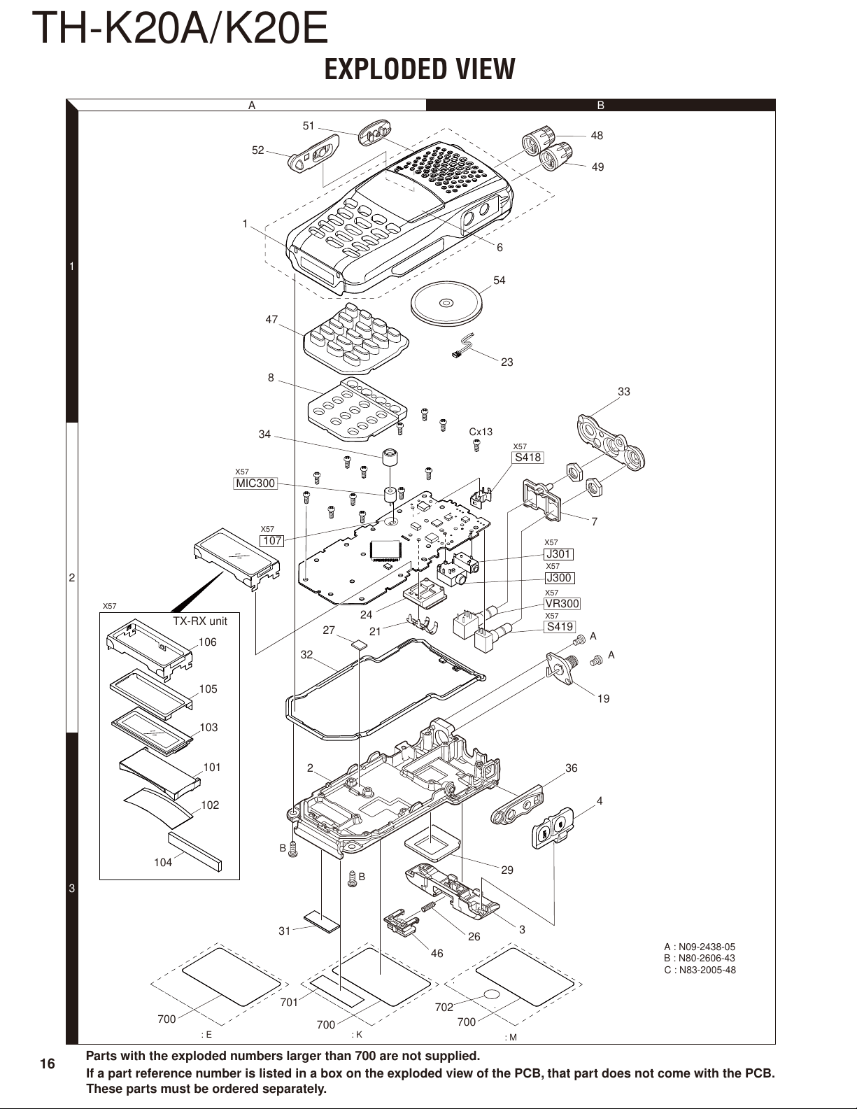
EXPLODED VIEW
BA
48
49
6
54
23
33
34
X57
MIC300
X57
107
2
X57
TX-RX unit
106
105
103
101
102
32
2
27
24
21
7
Cx13
X57
S418
X57
J301
X57
J300
X57
VR300
X57
S419
36
7
A
A
19
4
16
B
104
3
31
701
700
700
B
46
702
700
: K : E
26
29
: M
3
A : N09-2438-05
B : N80-2606-43
C : N83-2005-48
Parts with the exploded numbers larger than 700 are not supplied.
If a part reference number is listed in a box on the exploded view of the PCB, that part does not come with the PCB.
These parts must be ordered separately.

1
59 AC ADAPTER
(W08-1247-15): K
58 AC ADAPTER
(W08-1246-15): M, E
62 BATTERY ASSY
(W09-1073-25)
38 PACKING FIXTURE
(H12-4326-02): K
PACKING
11 INSTRUCTION MANUAL
(B62-2369-00): K, E
18 INSTRUCTION MANUAL
(B62-2375-00): M
712 WARRANTY CARD
711 PROTECTION BAG
TH-K20A/K20E
DC
9 INSTRUCTION MANUAL
(B62-2365-00)
12 INSTRUCTION MANUAL
(B62-2370-00): K, E
13~16 INSTRUCTION MANUAL
(B62-2371-00) : E
(B62-2372-00) : E
(B62-2373-00) : E
(B62-2374-00) : E
710 PROTECTION BAG
57 HELICAL ANTENNA
2
(T90-1044-15): K, E
56 HELICAL ANTENNA
(T90-1018-35): M
42 Belt clip
(J29-0756-05)
61 CHARGER
(W08-1249-35)
37 PACKING FIXTURE
(H12-4324-02): K
3
M: TH-K20A(M)
K: TH-K20A(K)
E: TH-K20E(E)
Parts with the exploded numbers larger than 700 are not supplied.
41 ITEM CARTON CASE
(H52-2486-02): K
17

TH-K20A/K20E
ADJUSTMENT
Note:
• When performing the TH-K20 adjustment, a personal
computer, programming interface cable (KPG-22A/22U),
tuning cable (E30-3216-05) and tuning software (MCP-5T)
are required.
• When you do not want to lose data such as memory
channels or menu items, save the data using the MCP-
5A (Memory control program), then write the data to the
transceiver after performing the adjustment.
To download the MCP-5A software, go to:
http://www.kenwood.com/i/products/info/amateur/software_download.htm
(This URL may change without notice.)
1. PC Tuning
The tuning software can be used with a PC. Figure 1
shows the setup of a PC for programming.
PC
MCP-5T
KPG-22A or KPG-22U
Illustration is KPG-22A.
Required Test Equipment
1. Stabilized Power Supply
1) The supply voltage can be changed between 3V and 16V
and the current is 3A or more.
2) The standard voltage is 7.5V. (Power supply voltage
range: 6V-9V)
2. DC Ammeter (DC. A)
1) Class 1 ammeter (17 ranges and other features)
l
2) The full scale can be switched between 300mA and 3A.
3) A cable with low internal loss must be used.
3. Frequency Counter (f. counter)
1) Frequencies of up to 1GHz or so can be measured.
2) The sensitivity can be changed to 250MHz or below and
measurements are highly stable and accurate (about
0.2ppm).
4. Power Meter (terminal type)
1) Measurable frequency: Up to 500MHz
2) Impedance: 50, unbalanced
3) Measuring range: Full scale of 10W
4) The specifi ed special connection cable must be used.
5. RF VM (RF V.M)
1) Measurable frequency: Up to 500MHz or so
KPG-22A
+
SP
–
+
MIC
–
PC
USB
KPG-22U
Tuning cable
(E30-3216-05)
Gray
Gray/Black
1.5D-XV Lead wire
1.5D-XV Shield wire
D-SUB
(9-pin)
Transceiver Transceiver
Fig. 1
PC
Note:
• You must install the KPG-22U driver in the computer to
use the USB programming interface cable (KPG-22U).
The KPG-22U driver runs under Windows XP, Vista or 7.
2. Tuning Software MCP-5T Description
The MCP-5T is the tuning software for the TH-K20. This
software runs under Windows XP, Vista or 7 on a PC. The
software allows a user to tuning the transceiver via Program-
ming interface cable (KPG-22A/22U) and tuning cable (E30-
3216-05).
Refer to the MCP-5T help fi le for the details on how to
use the MCP-5T.
3. Firmware version information
Press and hold the [ENT] key while turning the transceiv-
er power ON , the fi rmware version information appears on
the LCD.
6. Linear Detector
1) Measurable frequency: Up to 500MHz
2) Characteristic is fl at and CN is 60dB or more.
7. Digital Voltmeter
1) Voltage range: FS = 18V or so
2) Input resistance: 1M or more
8. Oscilloscope
1) Measuring range: DC to 30MHz
2) Provides highly accurate measurements for 5 to 25MHz
9. AF Voltmeter (AF V.M)
1) Measurable frequency: 50Hz to 1MHz
2) Maximum sensitivity: 1mV or more
10. Spectrum Analyzer
1) Measuring range: 10kHz to 1GHz or more
11. Standard Signal Generator (SSG)
1) Maximum frequency: 500MHz or more
2) Output: –133dBm (0.05µV) to –13dBm (50mV)
3) Output impedance: 50
12. Tracking Generator
1) Center frequency: 50kHz to 200MHz
2) Frequency deviation: ±35MHz
3) Output voltage: 100mV or more
13. Dummy Load
1) 8, 3W or more
18

ADJUSTMENT
TH-K20A/K20E
Frequency and Signaling
The transceiver has been adjusted for the frequencies
shown in the following table. When required, re-adjust them
following the adjustment procedure to obtain the frequencies
you want in actual operation.
Test Frequency
■
CH Receive (MHz) Transmit (MHz)
1 159.05000 159.10000
2 144.05000 144.10000
3 173.95000 173.90000
4 159.00000 159.00000
5 159.20000 159.20000
6 159.40000 159.40000
7~16 - -
Signaling
■
No. RX (Decode) TX (Encode)
1 None None
2 None 100Hz Square Wave
3 CTCSS 67.0Hz CTCSS 67.0Hz
4 CTCSS 151.4Hz CTCSS 151.4Hz
5 CTCSS 210.7Hz CTCSS 210.7Hz
6 CTCSS 254.1Hz CTCSS 254.1Hz
7 DCS D023N DCS D023N
8 DCS D754I DCS D754I
9 None
10 None
11 None 1633Hz Tone
DTMF
(Code: 159D)
DTMF
(Code: D)
Preparations for Tuning the Transceiver
Before attempting to tune the transceiver, connect the
unit to a suitable power supply.
Whenever the transmitter is tuned, the unit must be con-
nected to a suitable dummy load (i.e. power meter).
The speaker output connector must be terminated with a
8 dummy load and connected to an AC voltmeter and an
audio distortion meter or a SINAD measurement meter at all
times during tuning.
Tuning frequency
■
Tuning point Receive (MHz) Transmit (MHz)
Low 136.05000 136.10000
Center 146.05000 146.10000
Center*1 155.05000 155.10000
High 173.95000 173.90000
*1: This center frequency is used for adjustment of DCS Balance
and Maximum Deviation.
Adjustment Points
TX-RX UNIT
Component side view
MIC300
+B
BATT+
SPK
SPG
GND
BATT-
CN300
CV
ANT
Foil side view
S417
S418
PTT
POW/VOL
VR300
BATT+ (7.5V)
S419
SP
+
–
ENCODER
J301
Note: When replacing CF200 and C
MIC
J300
MONI
CF200
CD200
D
200, apply bond to
the point shown in the fi gure.
BATT– (GND)
19

TH-K20A/K20E
Common Section
Item Condition
1. Setting 1) BATT terminal voltage: 7.5V
2) SSG standard modulation
[Wide]
MOD: 1kHz, DEV: 3kHz
[Narrow]
MOD: 1kHz, DEV: 1.5kHz
Test-
equipment
ADJUSTMENT
Measurement Adjustment
Unit
Terminal
Unit Parts Method
Specifi cations / Remarks
2. VCO Lock
Voltage
Note:
• Press [Apply] button to store the adjustment value. (For single adjustment point)
• Press [Apply All] button to store the adjustment value after all adjustment points have been adjusted. (For 3 adjustment point)
1) Adj item: High Power
meter
TX-RX ANT
(CV)
MCP-5T4.0V
[V] indicator on the
PC window shows
VCO lock voltage.
Change the adjust-
ment value to get
VCO lock voltage
within the limit of the
specifi ed voltage.
±0.1V
Press [Apply] button to store
the adjustment value.
Transmitter Section
Measurement Adjustment
Item Condition
1. Frequency 1) Tuning point: High
Press [Transmit] button.
2. High
Transmit
Power and
Protective
Current
3. Low
Transmit
Powe r
1) Tuning point: Low, Center,
High (3 points)
BATT terminal voltage: 7.5V
Press [Transmit] button.
1) Tuning point: Low, Center,
High (3 points)
BATT terminal voltage: 7.5V
Press [Transmit] button.
Test-
equipment
f. counter TX-RX ANT MCP-5T173.900MHz ±50Hz
Powe r
meter
Ammeter
Unit
Terminal
Unit Parts Method
MCP-5T5.5W ±0.1W
1.0W ±0.1W
Specifi cations / Remarks
2.0A or less
1.0A or less
4. Mid
Transmit
Powe r
5. DCS
Balance
[Wide]
6. Maximum
Deviation
[Wide]
20
1) Tuning point: Low, Center,
High (3 points)
BATT terminal voltage: 7.5V
Press [Transmit] button.
1) Tuning point: Low, Center,
High (3 points)
(Signaling Square Wave)
Deviation meter fi lter
LPF: 3kHz
HPF: OFF
Press [Transmit] button.
1) Tuning point: Center, Low,
High (3 points)
AG: 1kHz/150mV
Deviation meter fi lter
LPF: 15kHz
HPF: OFF
Press [Transmit] button.
Powe r
meter
Deviation
meter
Oscilloscope
AG
AF VM
TX-RX ANT
SP/MIC
connector
2.0W ±0.1W
MCP-5TMake the modulation
wave into square
waves.
4.0kHz
(According to
the larger +, –)
1.5A or less
±100Hz

TH-K20A/K20E
ADJUSTMENT
Measurement Adjustment
Item Condition
7. Battery
Detection
Check
(User mode)
• This transceiver is designed to make adjustments simple.
• It is not necessary to adjust the fi xed values for the DTMF-DEV, DQT-DEV, QT-DEV, and MIC sensitivity.
• The TX-DEV Narrow setting uses the Wide calculated adjustment level value.
1) BATT terminal voltage: 7.1V
PTT: ON
TX Power: Low
Battery type: Li-ion
2) BATT terminal voltage: 7.8V
PTT: ON
TX Power: Low
Battery type: Li-ion
Receiver Section
Item Condition
1. Band Pass
Filter
2. Sensitivity
Check
[Narrow]
1) Tuning point: Low, Center,
High (3 points)
SSG output: –90dBm
(7.08µV)
SSG DEV: 3.0kHz
1) Tuning point: Low, High
(2 points)
SSG output: –120dBm
(0.22µV)
SSG DEV: 1.5kHz
Test-
equipment
Powe r
meter
DVM
Test-
equipment
SSG
DVM
Oscilloscope
AF VM
Unit
Terminal
TX-RX ANT
BATT
terminal
Measurement Adjustment
Unit
Termina
TX-RX ANT
SP/MIC
connector
Unit Parts Method
l Unit Parts Method
Check Segment display: 4 dots
MCP-5T[Automatic Adjust-
ment]
Press [Start] button
of “Auto Tuning”.
Press [Apply] button
to store the adjust-
ment value after the
automatic adjust-
ment has fi nished.
Check 12dB SINAD or more
Specifi cations / Remarks
Segment display: 9 dots
Specifi cations / Remarks
3. Squelch
Level 2 Write
[Wide]
[Narrow] 2) Tuning point: Low, Center,
4. S Meter 1
Write
(RSSI)
S Meter
FULL Write
(RSSI)
• The Squelch Level 1 setting uses the Squelch Level 2 calculated adjustment level value.
1) Tuning point: Low, Center,
High (3 points)
SSG output: –121dBm
(0.2µV)
SSG DEV: 3.0kHz
High (3 points)
SSG output: –121dBm
(0.2µV)
SSG DEV: 1.5kHz
1) Tuning point: Center
(1 points)
SSG output: –120dBm
(0.22µV)
SSG DEV: 3.0kHz
2) Tuning point: Center
(1 points)
SSG output: –105dBm
(1.26µV)
SSG DEV: 3.0kHz
MCP-5TWrite
MCP-5TWrite S Meter Icon (2 dots)
Write S Meter Icon (9 dots)
21

4
5
TH-K20A/K20E PC BOARD
1
TX-RX UNIT (X57-821X-XX) 0-11: K 0-20: M 2-71: E
2
Component side view (J79-0325-09)
J79-0325-09
JIHGFEDCBA
D41
3
R448
D419
D418
4
D416
D410
D411
D406
D420
D422
76
75
D407
CN202
25
IC401
26
CN304
CN30
100
1
5R
Q400
R422
C412
C411
F424
R447
D417
R425
X400
C415
D409
D408
D405
D421
5
D404
6
R449
R450
D423
CV
7
8
10
11
12
13
R451
D425
R433
R432
R431
D424
MODE
GND
RESE
9
D41
Ref. No. Address
IC300 6O
IC301 8Q
IC304 6P
IC305 6M
IC306 5N
IC307 4P
IC308 4N
IC401 6J
Q300 6Q
Q301 5P
Ref. No. Address
Q302 5P
Q303 4O
Q304 7N
Q305 4O
Q306 5P
Q308 4N
Q400 7H
D300 8O
D301 5M
D302 5N
Ref. No. Address
D304 5N
D305 9O
D404 5C
D405 5D
D406 5E
D407 5F
D408 5D
D409 5E
D410 5E
D411 5E
Ref. No. Address
D414 10J
D415 2J
D416 4G
D417 8G
D418 3F
D419 3D
D420 5F
D421 5D
D422 7F
D423 7D
Ref. No. Address
D424 9F
D425 9D
D426 8R
D427 7R
14
22

J KLMNOPQRS
N304
GND
D415
CN303
RESET
PC BOARD TH-K20A/K20E
1
TX-RX UNIT (X57-821X-XX) 0-11: K 0-20: M 2-71: E
Component side view (J79-0325-09)
R440
C423
R443
MIC300
C344
R377
D301
C380
C352
F300
+B
+B
GND
IC305
2
1
C365
1
2
C364
C363
SPK
SPG
C354
51
50
CP1
5M
4
3
C358
CN300
C383
1
3
4
5
C366
R362
C329
IC308
IC306
5M
Q304
5T
S
R379
D304
D302
3
1
D
Q308
D
G
C377
5
C375
4
SB
R372
G
C322
C321
R323
R358
R351
R365
R364
S
R355
R363
5C
C376
C374
R374
GND
R305
C304
R309
R350 and
C356
R360
D305
Q305
G
Q303
C359
S
C301
D
S
G
D
C367
C369
18
19
IC300
24
1
R300
R301
D300
C351
R354
C353
R370
13
6
R302
C302
R310
C307
12
7
R308
R368
R304
R376
6
10
Q302
C305
R307
R303
C306
R366
C373
IC307
Q301
R359
C372
C379
5
1
R378
C360
R367
SB
R335
R337
R336
C333
C336
R338
C334
1
R339
45
C342
R340
R345
R346
C314
R347
C340
R353
IC304
C339
R342
C341
R318
Q306
D
G
S
F301
C332
C337
C338
C381
8
R341
R317
C313
C421
R441
R316
D
Q300
C312
R315
C310
R312
5
8
R313
R357
R470
C311
IC301
R389
R314
C308
C371
C335
R311
C425
R380
R445
R446
D427
4
1
D426
R466
2
3
4
5
6
7
8
9
D414
Component side
Layer 1
Layer 2
Layer 3
Layer 4
10
11
Foil side
12
13
23
14

R235
3
R127
3
3
2
L211
6
TH-K20A/K20E PC BOARD
1
TX-RX UNIT (X57-821X-XX) 0-11: K 0-20: M 2-71: E
2
Foil side view (J79-0325-09)
JIHGFEDCBA
S418
PTT
S417
MONI
3
C125
R126
C157
D102
R128
D101
L108
C144
L112
C135
C134
D103
D105
R119
L107
C146
D104
L115
C133
C265
C139
C141
4
L110
C140
C138
L109
C137
C136
5
R319
C318
R388
R320
C345
6
VR300
+
C357
7
Q404
Q403
8
S419
C424
R453
R452
C347
J301
J300
C317
C320
R325
C325
5
4
IC302
1
8
R386
C319
R322
R326
C324
5
4
IC303
1
8
C328
R328
R385
R387
R321
C327
R327
R329
C326
R330
R361
C316
R369
C361
C406
C407
C404
C405
L214
L213
C261
C427
C428
C129
R243
8
1
R402
D203
C256
R241
R414
IC400
R415
L114
R405
5
4
C259
R240
C419
Q204
G
G
C255
R239
R238
C253
C417
C420
C160
C154
S
D
D401
R438
C127
R236
R439
C418
R437
Q402
R129
R237
L11
C25
R248
C38
R38
R3
C3
C251
R464
9
10
11
12
13
14
24
Ref. No. Address
IC1 8Q
IC200 8M
IC302 6G
IC303 7F
IC400 8I
Q1 6Q
Q2 4P
Q3 5Q
Q4 4Q
Ref. No. Address
Q5 3Q
Q6 8R
Q7 9Q
Q101 4N
Q102 3N
Q103 4L
Q104 4N
Q200 8M
Q201 9O
Ref. No. Address
Q202 8N
Q203 6M
Q204 6J
Q307 4O
Q401 9J
Q402 8J
Q403 8C
Q404 7C
D1 5P
Ref. No. Address
D2 5P
D3 6P
D4 5Q
D5 5Q
D6 5P
D7 4P
D8 3P
D9 5R
D10 6R
Ref. No. Address
D11 6Q
D101 4F
D102 4F
D103 4G
D104 5H
D105 4G
D200 6K
D201 6K
D203 5I
Q401
Ref. No. Address
D204 6L
D401 8J

J KLMNOPQRS
C417
C420
204
255
239
C154
C253
S
D
D401
C160
R438
Q401
C127
R236
R439
C418
R437
Q402
L113
R129
C254
R237
R248
C386
R382
C125
C251
R332
C331
R464
R444
R127
R235
L211
R442
C330
C250
R334
R125
D201
R383
R331
C249
R333
C247
R234
C248
R233
C402
R130
C151
D200
C246
R401
C162
C161
C152
R400
C245
C323
R403
C204
R324
L106
R121
C153
L209
TH101
R419
CD200
R251
C272
C413
C273
C203
R204
D204
C414
C271
R465
C270
Q103
R207
L217
R205
R232
R203
C211
GD
C244
C205
R201
C202
Q200
R115
C115
C150
R231
C207
R116
C240
R230
CF200
C206
R206
8
9
C209
PC BOARD
TH-K20A/K20E
TX-RX UNIT (X57-821X-XX) 0-11: K 0-20: M 2-71: E
Foil side view (J79-0325-09)
C105
C113
R246
R229
R252
R114
IC200
R112
R113
G
Q203
C208
C233
SG
D
C212
L105
F101
C214
R208
D
C112
C239
R253
C213
C108
L104
G
S
R108
Q102
R111
C109
C110
R109
C104
C155
C156
C159
Q104
R120
R124
R227
R225
C235
L206
R247
C237
R228
R226
R200
C200
C201
1
16
L202
R249
R210
R213
C221
C217
TH200
R215
C215
C107
C
E
C232
Q202
R104
C266
L205
C228
R220
C223
C106
Q101
R216
R103
C385
C234
R221
XF200
C216
C218
R212
R105
E
B
Q307
R43
L103
C227
R28
L200L201
R107
C148
C147
R101
C382
C231
R27
C48
R102
C102
L204
C230
C229
R41
C219
C220
C49
C44
C101
C384
+
L101
C226
Q201
L215
C38
C37
R24
C34
D8
R22
R26
L11
C36
R25
X1
C50
R214
R218
R11
C18
D2
C47
C21
C1
C33
D7
Q2
+
C16
D6
L2
D1
L5
L1
C6
D3
L3
16
C39
+
1
L13
C45
C51
R21
C32
Q5
C26
R23
C8
R39
R20
R19
C31
C13
C5
L4
Q3
R8
C7
D5
D4
Q1
R6
R5
R2
IC1
Q7
C43
C41
R15
C10
C17
C19
R12
C20
L10
C28
C25
C29
C27
L9
R14
Q4
R35
R34
C42
R48
S
D11
R45
D
C15
C46
C23
C22
R18
L6
L8
C2
C3
R3
R4
R7
R9
R33
R37
R38
R36
R31
R32
Q6
R30
R40
R46
R10
G
C9
C4
9
8
R47
1
2
3
4
C12
+
C11
D9
D10
5
6
7
8
9
J79-0325-09
Component side
Layer 1
Layer 2
Layer 3
Layer 4
10
11
Foil side
12
13
25
14

A
B
C D
E
TH-K20A/K20E
1
2
3
TX-RX UNIT(X57-821X-XX)
LCD
COM0
COM1
COM2
COM3
SEG0
47K
R470
INPTT
100
R441
PTT
S418
1000p
C421
MONI
S417
C423
1000p
SEG1
SEG2
SEG3
SEG4
R440
R443
SEG5
SEG6
47k
100
SEG7
SEG8
SEG9
SEG10
SEG11
SEG12
S401
9
S405
6
S409
3
S413
D
SEG13
SEG14
SEG15
SEG16
SEG17
SEG18
SEG19
S402 S403 S404
0
#
S406
S407
8
5
S411
S410
S414
1
S415
C
B
SCHEMATIC DIAGRAM
SEG20
SEG21
SEG22
SEG23
S408
S412
S416
SEG24
SEG25
SEG26
7
42
D4 04-407
A
REVERSE CURRENT
PREVENTION
SEG27
SEG28
D404
1SS388F
D405
1SS388F
D406
1SS388F
D407
1SS388F
R431
R432
R433
SEG29
SEG30
SEG31
D408-D411
D408
Key matrix
D409
D410
DA2S101
D411
DA2S101
0-20
0-11
2-71
X57-8210-XX
0-20
0-11
2-71
D408
M
K
DA2S101
E
DA2S101
DA2S101
NO
DA2S101
NO
KEYO4
KEYO3
KEYO2
KEYO1
KEYIT
KEYI4
KEYI3
KEYI2
KEYI1
MONI
NO
0
NO
0
NO
NO
NO
NO
0
5MS
5MSC
SPM
5CC
5TC
REM
R433
R432
R431
D409
DC SW
Q306
SSM6J08FU(F)
C379
47k
R377
C380
1000p
LAMP
LEDG
LEDR
ENC2
ENC1
C381
0.1u
220p
DC SW
LTA023JEBFS8
270p
C382
C371
DC SW
Q307
REM
27k
R378
R357
560
0.027u
SSM3J05FU-F
100k
R379
C385
C384
VOL OUT
2.2
R380
Q308
C383
1000p
1000p
1000p
R:4.89V
T: 1.59V
5MS
INPTT
RXD
EXPTT
TXD
5RC
RESET
5M
SB
+B
5C
5T
5TC
5R
5CC
5RC
12A02CH
Q402
C374
0.056u
R350
18k
1000p
R351
100
100p
Q401
R438
C357
100u
7.5V
PROTECT
C352
1000p
SB
CN305
D401
OVER VOLTAGE
LIMITTER
D401
680
6.3
D301
C417
DZ2S036(0)
GN1G
1000p
C419
C418
1000p
R355
470
R358
47k
R354
1k
C353
0.047u
R359
330
R353
10k
Q301
LTC044EEBFS8
DC SW
+B
REVERSE CURRENT
PREVENTION
D302
RB521S-30
R305
10k
OFF:0.40V
ON:5.57V
C420
10u
R360
1.8k
C356
10u
C358
1000p
R363
R361
47k
4.7u
R464
R439
1k
1NC
2 VSS
3CE
D414,D415
B30-2261-05
LCD BACKLIGHT
27k
D414
D415
33k
330
R442
R444
OFF: 0V
ON:2.75V
C359
0.01u
R364
1k
REM
C361
0.22u
LTC044EEBFS8
C360
0.22u
DC SW
VOLTAGE
REGULATOR/5V
IC306
XC6209B502P-G
VoUT
D416
D417
1.2k
R447
220
R365
2.2k
Q302
7.5V
REG
5
C365
1000p
4VIN
VOLTAGE
DETECTOR/RESET
D416-D425
B30-2337-05
KEY BACKLIGHT
D420
D418D419
D421
1.2k
R449
R448
RXD
EXPTT
TXD
REM
SB
330k
R367
R368
270k
C367
5.01V
10u
C366
C354
D423 D422
1.2k
1.2k
R450
C424
0.01u
SP MUTE SW
Q303
2SK3577-A
R370
470k
1u
C369
SPM
5M
SB
5MS
+B
SSM3J05FU-F
R362
330k
4
VIN
1000p
1NC
IC305
XC6120N302N-G
R372
D424
D425
R451
C425
R374
AF AMP
0.047u
47k
3
2 VSS
LED
GREEN
B30-1782-05
LED
RED
B30-1779-05
1.2k
0.01u
Q305
2SK3577-A
10k
ON:4.99V
OFF: 0V
Q304
VoUT
C363
D426
DC SW
Q403
RT1N144U-T111
D427
DC SW
Q404
RT1N144U-T111
R466
0
AF AMP
0
R366
C372
DC SW
5MSC
RESET
1u
C364
1000p
D304
REVERSE CURRENT
PREVENTION
R445
220
R446
330
ON:3.30V
OFF: 0.51V
C373
10u
D304
C375
F301
0.315A
100p
R376
0
RB521S-30
1u
C376
OFF:0V
ON:4.98V
OFF:0V
ON:5.02V
100k
R453
10 PoUT
9 PW-GND
8 PRE-GND
7 PHASE
6NF
AF POWER AMP
4.7u
C377
100k
R452
IC307
TA7368PL
NC1
VCC
NC2
VIN
RIPPLE
IC308
XC6209B502P-G
4VIN
5 VoUT
VOLTAGE
1u
REGULATOR/5V
GREEN LED
ON:5.0V
RED LED
ON:5.0V
CN303
AF AMP
ON:7.49V
OFF: 0.33V
1
2
3
4
5
SPG
3CE
2VSS
1NC
BACKLIGHT
LED SWITCH
R437
3.3k
BACKLIGHT
CONTROL
J300
SP
J301
SWITCH
2SC4617(R)
B
C
A
2
C344
270p
1
C351
D305
DZ2S068(M)
SURGE
ABSORPTION
PTT/RXD
1
MIC
3
11
IM
10
5MS
2
1
SPG
3
TXD/REM
SPK
4
AFO
2
C347
1000p
CN300
+
2
SPK
1
-
SPG
4
ENC
S419
MIC300
INT MICINT MICINT MIC
5
MIC
INT SP
6
+B
BATT+
BATTERY
TERMINAL
BATT
GND
POWER SW
/AF VOLIUM
F300
3.15A
-
C345
VR300
7
26
X57-821 1/4
X57-821 1/1

F G H I
SCHEMATIC DIAGRAM
TH-K20A/K20E
J
TX-RX UNIT (X57-821X-XX)
5MS
5MSC
SPM
5CC
5TC
C330
SB
C331
REM
5MS
INPTT
270p
R332
270p
R331
56k
56k
R400
C386
220k
0.047u
R333
R334
R401
R403
R382
SHIFT
THERM
5VC
SPM
DAT
5CC
CLK
MONI
5MSC
71
72
73
74
75
CLK
5CC
76
77
78
79
47k
47k
KEYO4
C402
KEYO3
1000p
KEYO2
220k
KEYO1
220k
R383
8.2k
10k
KEYI1
KEYI2
KEYI3
KEYI4
KEYIT
KEYIS
80
81
82
83
84
85
86
87
88
89
90
91
92
93
94
95
96
97
98
99
100
DATA
5TC
VOLCS
VDCSW
CURRENT
VOX
REM
BATT
THERM
RSSI
SQL
LSDI
CVDET
KEYO4
KEYO3
KEYO2
VL1
VL2
VL3
SHIFT
KEYO1
VL4
KEYI1
KEYI2
KEYI3
KEYI4
KEYIT
KEYIS
HSDO
123456789
CN304
HSDO
MONI
LSDO
SPM
WKUPO
5MSC
VREF
5VC
MODE
SHIFT
THERM
CURRENT
LSDI
VOX
5MS
DAT
CLK
VDCSW
VOLCS
5VC
SEG30
SEG29
SEG28
SEG27
SEG26
SEG25
SEG24
SEG23
SEG26
BSFT
SEG25
INPTT
596061
SEG24
5RC
58
ENC2
SEG22
57
SEG23
ENC1
LEDG
LEDR
SEG31
62
63
64
65
66
67
686970
LEDR
LEDG
SEG31
XCIN
XCOUT
RESET
101112131415161718192021222324
47k
R465
SEG27
SEG28
SEG29
SEG30
MCU
IC401
R5F2L3ACCKEKA
XOUT
VSS
XIN
VCC
SEG21
56
SEG22
SEG21
RxD
SEG20
55
SEG20
TxD
SEG19
SEG18
SEG17
SEG16
51
525354
SEG16
SEG17
SEG18
SEG19
SEG15
SEG14
SEG13
SEG12
SEG11
SEG10
SEG9
SEG8
SEG7
SEG6
SEG5
SEG4
SEG3
SEG2
SEG1
SEG0
COM3
COM2
COM1
COM0
E2PIN
E2PCS
NC
LAMP
EX
PTT
W/N
PLLEN
PLLPS
PLLLD
25
SEG15
50
SEG14
49
SEG13
48
SEG12
47
SEG11
46
SEG10
45
44
43
42
41
40
39
38
37
36
35
34
33
32
31
30
29
28
27
26
CP1
SEG9
SEG8
SEG7
SEG6
SEG5
SEG4
SEG3
SEG2
SEG1
SEG0
COM3
COM2
COM1
COM0
LAMP
SHIFT
THERM
CURRENT
VDCSW
5MS
PLPS
PLLLD
DAT
CLK
PLLE
LSDI
VOLCS
5C
5RC
RESET
22u
22u
22u
8
7
6
5
CN311
CN308
C404
GND
22u
5.0V
C407
4.7k
R414
4.7k
R415
4.7k
R402
CLK
DAT
EXPTT
CN306
CN400
CN402
+B
C405
C406
4.7k
R405
5C
EEPROM
C427
RXD
EXPTT
TXD
E2PIN
E2PCS
LSDO
CVDET CVDET
CN310
CN309
7.51V
5T
5T
5M
SB
+B
5C
5T
5R
RSSI
SQL SQL
C428
IC400
EX25064ATA00A
1S
2Q
3W
4 VSS
5M
SB
CN307
1000p
0.01u
VCC
HoLD
C
D
5M
GND
RESET
CN401
R419
4.7k
MODE
CN403
1k
R422
C412
1p
12p
C411
Q400
2SC4649(N,P)
SWITCH
C413
0.1u
C414
1000p
L77-2974-05
11.0592MHz
X400
R424
1k
RSSI
5T
CN312
C415
5R
12p
R425
5.01V
470k
5RC
ENC2
ENC1
+B
CLK
5C
C341
R346
C342
0.01u
270k
1000p
R347
47k
DAT
LSDO
5VC
VOX
W/N
RSSI
SQL
5R
5T
EXPTT
E2PCS
E2PIN
+B
C340
R345
82k
0.01u
27
X57-821 1/1
X57-821 2/4

K L M
N
O
TH-K20A/K20E
SHIFT
THERM
VDCSW
5MS
PLPS
PLLD
DAT
CLK
PLLE
5C
LSDI
VOLCS
+B
LSDO
CVDET
5VC
VOX
5R
W/N
RSSI
5T
SQL
R41
MOD
3.9k
R303
10k
CV
FREQUENCY
CONTROL
D11
C37
R47
10k
R304
220n
C1
VCO
SPEED UP
C3
1u
C2
0.033u
R48
1k
D11
DA2S101
R27
2.2k
R28
0.15u
C38
D9
1M
L1
0.18u
D1,2
15k
1k
R4
R3
D1
820
C39
10
6.8u
R30
D10
DA2S101
R300
R301
R302
1SV325F
D3
RF SWITCH
D2
L2
180n
1SV325F
R5 1k
R2 2.7k
C4 0.022u
0.68u 20
R31
10k
10k
R32
Q6
LTC014EEBFS8
DC SW
DA2S101
CURRENT
STEERING
D/A CONVERTER
1
VIN2
2
VDD
1k
3
LD
1k
4
CLK
1k
5
DI
6
VIN3
0.047u
R308
1k
0.1u
C302
D4
MODULATOR
C5
39 p
C6
L3
10u
0.022u
C8
D3
1000p
Q1
LTC014EEBFS8
R6
100k
10k
10k
10k
10k
R34
R35
R33
23
24
VoUT1
VoUT2
R2A20178NP2
IC300
VoUT38VoUT49VIN410VIN511VoUT512VoUT6
7
C304
39 k
C307
R310
L4
27n
D4
L5
22n
HSC277
SHIFT
C9
PLL SYSTEM
MB15E03SL-E1
9 CLoCK
10 DATA
11 LE
12 PS
13 ZC
14 LD/FoUT
15 P
16 R
R36
R37
R38
19
20
21
VIN822VIN1
VoUT8
RESET
VDAREF2
VDAREF1
5.6k
R309
CURRENT
STEERING
KDR731
0.22u
D300
HVC350B
1u
IC1
oSCoUT
oSCIN
10k
10k
10k
VIN7
VoUT7
GND
VIN6
D5
FREQUENCY
CONTROL
C7
0.5p
R8
10k
R9
100k
R7
100k
C11
FIN
XFIN
GND
Do
VCC
VP
18
17
16
15
14
13
C306
1u
DATA
C305
1000p
8
7
6
5
4
3
2
1
CLK
1u
C301
R18
PLLEN
5MS
C10
L6
10u
D5
0
C12
Q1
TX/RX SW
R39
1000p
C41
0.1u
MCH3914(7)-H
8p
HVC350B
6.3
1u
5MS
10
C42
C43
0.01u
C44
1M
R307
SCHEMATIC DIAGRAM
VCO
C15
C17
C13
C46
1000p
0.01u
T0
1000p
Q3
10p
C19
L8
10u
9p
R12
220
Q2
2SC5383-T111
C18
1000p
C16
22u 10
4.98V
56
R40
2SC5383-T111
2.90V
C45
22p
TCXO
X1
19.2MHz
VCoNT
GND
oUTPUT
L77-3074-05
+B
5C
LSDI
POWC
BPF
C316
R319
C318
1k
R388
0.18u
R10
22
0.01u
C20
1000p
RIPPLE FILTER
D6
1000p
D6
SPEED UP
THERM
CURRENTCURRENT
VDCSW
VOLTAGE
REGULATOR/3V
Q7
VCC
0.18u
C317
180
R335
10k
R336
C332
R15 47k
0.70V
Q4
2SC5108(Y)F
C22
0.5p
RF BUFFER
4.15V
C23
R11
4.7k
DA2S101
10
R43
C48
0.01u
L13
4.7n
4p
C47
AF FILTER
IC302
NJM12904RB1
8V+
0.1u
7 BoUT
6 B-IN
5 B+IN
R320
56k
LTA023JEBFS8
5MS
R337
10k
10k
C333
8200p
1u
5R
W/N
RSSI RSSI
SQL SQL
R369
R14
1000p
C21
R45
R46
C49
AoUT
A+IN
0
Q300
C334
A-IN
GND
10k
1k
33k
100k
1000p
C335
0.027u
R338
1000p
C50
R339
C336
1
2
3
4
270p
5p
R321
1k
L9
C25
R389
R311
R386
R387
2.2k
DC SW
MIC AMP/LIMITER
NJM12904RB1
1
4
820p
120n
1000p
C26
C51
22p
82k
GND
C337
C338
15k
47k
33k
-
C27
47p
R313
R385
1k
R322
3.3k
C319
0.18u
IC304
+
C28
9p
L10
27n
15p
R312
C29
47k
47k
C308
R:1.80V
T:1.81V
V+
-
+
0.01u
1000p
1.80V
15p
0.1u
C321
C320
0.18u
5VC
8
5
C31
12p
LSD BUFFER
IC301
NJM12904RB1
1
2
-
3
4
GND
1k
R323
0.18u
C322
0.39u
R325
470
C324
0.18u
1k
R340
R19
R20
++-
C325
RF AMP
5.6k
2SC5636
3.3k
R21
V+
R:4.89V
T: 1.59V
0.1u
R326
5.6k
R342
560k
C339
10p
R341
Q5
C32
330
1000p
5MS
C310
8
7
R315
6
560k
5
C311
820k
R314
QT/DQT FILTER
IC303
NJM12904RB1
8V+
7
6
-++
5
0
TX-RX UNIT (X57-821X-XX)
C34
15p
82n
L11
3.3k
R22
C33
10
R23
1000p
5C
5.0V
0.1u
C312
4700p
0.027u
R316
R317
LSDI
5MS
R328
10k
R329
330k
1
C326
180p
R327
2
-
GND
100k
3
4
R24
TX/RX SW
10k
C313
R318
3.9k
C314
5R
C327
D8
HSC277
D7
HSC277
3.3k
D7,8
0.1u
2.7k
0.01u
C328
4700p
R:1.03V
T:1.74V
R330
C329
R25
5R
0.01u
100k
2.2u
10k
R:4.88V
T: 1.59V
CURRENT
VDCSW
TCXO OUT
RXLO
THERM
POWC
BPF
W/N
+B
5R
5T5T
28
X57-821 3/4
X57-821 1/1

P Q R S T
SCHEMATIC DIAGRAM
TH-K20A/K20E
TX-RX UNIT (X57-821X-XX)
RXLO
THERM
5T
CURRENT
RFM01U7P
10
Hi:1.49V
R108
Mid:1.28V
Lo:1.21V
100k
R109
R26
C36
DRIVE
Q102
R111 82k
Hi:3.25V
Mid:2.78V
Lo:2.63V
4.7k
1000p
1000p
C109
C101
1
L110
C136
1000p
D101,102,103,104
ANT SW
270
L112
9T
22p
C144
R: 0V
T:4.93V
C156
330
C137
D105
1000p
L109
C138
C159
9T
6p
12p
C139
D103
RN142S
2.2u
C140
27p
R: 0V
T:0.81V
R119
0
RN142S
C141
ANT
CN2
12p
9T
6p
2
18p
D104
C146
RN142S
3
1000p
C135
C157
6p
L108
1000p
HVC131
HVC131
R126
D101
D102
2.2u
270
R128
R124
FINAL
Q103
68k
1000p
R114
R115
47
Hi:1.48V
Mid:1.27V
Lo:1.21V
56k
R102
RD07MUS2BT112
R116
0
Temp compensation
C153
C115
1000p
R103
2.2k
Q101
2SC4926YD
PRI DRIVE
R:0V
1k
T:0.61V
C104
1000p
R: 0V
T:4.91V
1000p
R104
100k
-t
B57331V2104J
TH101
18
R121
R105
C105
39 k
330
1000p
C161
C151
L103
R107
C147
100n
R: 0V
T:4.32V
18
1u
C113
56p
47
82n
L105
R112
F101
C112
0.01u
L101
68n
C102
1000p
0.5A 32V
R113
C150
R: 0V
T:1.09V
R101
18
0.1u
C110
22p
0.01u
2.2u
C162
C152
C148
1000p
1000p
C106
1000p
L106
R130
L113
3T
9T
0
C107
1000p
9p
C125
L114
L115
5T
47p
39 p
C127
C108
L104
15p
POWC
15p
C129
33n
CURRENT
R120
1.8k
C134
L107
6T
6T
1000p
27p
C133
C154
VDCSW
TCXO OUT
+B
POWC
BPF
5R
W/N
RSSI
5T
SQL
RXLO
C323
R324
560
3300p
R200
R232
47
0
C200
L217
5R
82n
R201
10u
C202
C272
C271
1p
C270
D204
C201
1000p
1.5k
C205
0.01u
LTA023JEBFS8
3p
39 p
HVC350B
R203
C203
R204
C204
0.1u
W:0V
N:5.01V
C273
1p
1M
R251
R252
4.7k
C206
270p
C207
270p
68k
IC200
TA31136FMG
270p
3.3k
R205 2.2k
L79-1474-05
1800p
CD200
Q200
W/N
2p
82n
L209
C245
D200,201,204
BPF TUNING
C208
330k
R206
8
FILIN
AFoUT
9
C209
R207
W/N SW
C246
D200
C211
FILoUT
QUAD
47p
2.7k
RSSI
39 p
1M
HVC350B
R233
L72-1042-05
CF200
0.1u
0.1u
IFIN
DEC
IFoUT
C248
1p
VCC
RSSI
C212
SQL
C249
1M
D201
R234
C247
1000p
450kHz
C213
MIXoUT
NOISEREC
NOISEDET
C214
0.033u
18k
R208
39 p
HVC350B
R253
4.7k
0.1u
1
OSCoUT
GND
16
0.1u
R210
68k
C250
C215
0.01u
OSCIN
MIXIN
7.5V
82n
L211
R248
2p
47
R235
C251
C254
1000p
C218
5p
22p
560n
L200
C216
FM IF
SYSTEM
R249
C217
1k
0.01u
TH200
NCP18WM474J0S
-t
R:4.88V
T: 1.59V
R236
82
1.5k
1000p
R:4.68V
T: 1.53V
L201
R212
C253
560n
100
L202
R213
1000p
C219
C220
820n
C221
47
Q204
3SK318
R237
DOUBLER
22p
1000p
0.01u
470
R214
330k
Q201
KTC4080E-P
R:0.72V
T: 0.71V
R216
180k
Q202
KTC4080E-P
0
R215
RF AMP
R240
BPF
IF AMP
100k
R238
R:4.88V
T: 1.59V
TCXO OUT
R:0.61V
T: 0.59V
R218
1k
C223
0.01u
100k
R:3.85V
T: 1.26V
R239
R220
680
39 0k
C255
1000p
L71-0669-05
1st IF(38.85MHz)
XF200
VDCSW
R:4.98V
T: 0V
R241
C226
R:3.11V
T: 1.03V
180k
C227
8p
5R
R221
330
LTC014EEBFS8
C256
47p
R243
C259
L215
2.7n
C228
0.01u
6p
C234
Q104
C155
VDC SW
1M
1000p
BPF TUNING
L206
R225
0.01u
C261
D203
C229
R226
820n
47
1000p
5p
0
39 p
L213
L214
HVC350B
L204
22n
C230
10p
3.3k
R247
C235
1000p
68n18n
C231
C237
R125
CN202
R227
C266
R228
22p
0.39
0.39
R129
0.39
R127
C160
1000p
4
C265
47p
5
3p
100p
C232
5p
120n
L205
C233
1000p
R:2.68V
T: 0.89V
1k
MIXER
Q203
3SK318
330
C239
1000p
R229
C240
82k
1000p
R230
R246
R:2.44V
T: 0V
82k
R231
100k
C244
6
1000p
82k
7
Note : The components marked with a dot (•) are parts of layer 1.
29
X57-821 1/1
X57-821 4/4
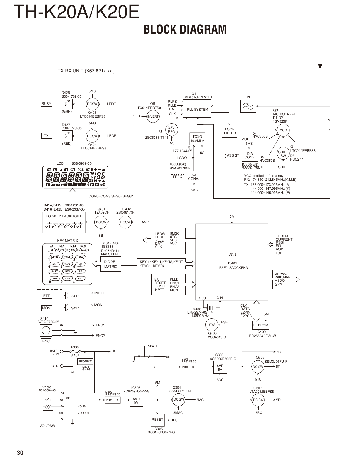
TH-K20A/K20E
TX-RX UNIT (X57-821x-xx )
BLOCK DIAGRAM
D426
B30-1782-05
BUSY
(GRN)
D427
B30-1779-05
TX
(RED)
B38-0939-05
LCD
D414,D415 B30-2261-05
D416~D425 B30-2337-05
LCD/KEY BACKLIGHT
KEY MATRIX
PTT
MONI
S419
W02-3766-05
ENC
BATT+
7.5V
BATT-
VR300
R31-0684-05
VOL/PSW
S418
S417
F300
3.15A
SB
5MS
DCSW
Q403
LTC014EEBFS8
5MS
DCSW
Q404
LTC014EEBFS8
COM0~COM3,SEG0~SEG31
PROTECT
D301
GN1G
VOLIN
VOLOUT
LEDG
LEDR
Q401
12A02CH
DCSW DCSW
SB
INPTT
MON
ENC1
ENC2
D404~D407
1SS388
D408~D411
MA2S111-F
DIODE
MATRIX
+B
D302
RB521S-30
PROTECT
2SC4617(R)
Q6
LTC014EEBFS8
PLLD
INVERT
2SC5383-T111
Q402
LAMP
LEDG
LEDR
PLLE
DAT
CLK
KEYI1~KEYI4,KEYIS,KEYIT
KEYO1~KEYO4
BATT
RESET
EXPTT
INPTT
BATT
IC306
XC6209B502P-G
AVR
5V
5M
RESET
IC305
XC6120N302N-G
Q7
SB
MB15A02PFV2E1
PLPS
PLLE
DAT
CLK
LD
3.3V
REG
5C
L77-1944-05
LSDO
IC300(6/8)
R2A20178NP
FREQ
5MSC
5TC
5RC
5CC
PLLD
ENC1
ENC2
MON
D304
RB521S-30
PROTECT
Q304
SSM3J05FU-F
DC SW
5MSC
RESET
IC1
PLL SYSTEM
TCXO
19.2MHz
X1
5C
D/A
CONV.
5MS
XOUT
X400
L78-2974-05
11.0592MHz
5MS
LOOP
FILTER
ASSIST
MCU
IC401
R5F2L3ACCKEKA
XIN
BSFT
SW
Q400
2SC4919-S
IC308
XC6209B502P-G
AVR
5V
5CC
LPF
D4
HVC350B
MOD
5MS
D/A
CONV.
D5
HVC350B
IC300(5/8)
R2A20178NP
VCO oscillation frequency
RX: 174.850~212.845MHz(K,M,E)
TX: 136.000~173.995MHz (M)
144.000~147.995MHz (K)
144.000~145.995MHz (E)
5M
CLK
DATA
E2PIN
E2PCS
EEPROM
IC400
BR255640FV1-W
Q308
DC SW
5TC
Q307
LTA023JEBFS8
DC SW
5RC
Q3
MCH3914(7)-H
D1,D2
1SV325F
VCO
SHIFT
SW
SHIFT
THREM
CURRENT
RSSI
SQL
VOX
LSDI
VDCSW
WIID/NAR
HSDO
SPM
5M
5C
SSM3J05FU-F
5T
5R
Q1
LTC014EEBFS8
D3
HSC277
2
30

TH-K20A/K20E
BLOCK DIAGRAM
RX: 136.000~173.995MHz (K,M,E)
TX: 136.000~173.995MHz (M)
144.000~147.995MHz (K)
144.000~145.995MHz (E)
D103-D105
+B
RF
5R
RN1425
D101,D102
HVC131
ANT SW
RF BPF
TUNE
IC300(7/8)
R2A20178NP
5T
BPF
-t
TH101
THREM
D203
HVC350B
ANT
Q4
2SC5108(Y)F
BUFF
AMP
S8
RIPPLE
FILTER
5C
19.2MHz
WID/NAR
2SC5636
Q2
2SC5383-T111
D6
DA2S101
Q201
KTC4080E-P
DOUBLER
5R
SQL
RSSI
L79-1474-05
LTA023JEBFS8
Q5
RF
AMP
5C
CD200
DC SW
Q200
2nd Local
38.4MHz
AFO
D7,D8
HSC277
TX/RX
SW
5T
5R
IC200
TA31136FMG
IF SYSTEM
CD
L72-1042-05
Q101
2SC4926YD
PRE
DRIVE
5T
VDCSW
1st Local frequency
174.850~212.845MHz(K,M,E)
5R
CF200
VDC SW
Q104
LTC014EEBFS8
Q202
KTC4080E-P
IF
AMP
5R
Q102
RFM01U7P
DRIVE
AMP
MCF
38.85MHz
XF200
L71-0669-05
RD07MUS2BT112
F101
0.5A
IC300(8/8)
R2A20178NP
POWC
MIXER
5R
Q103
FINAL
AMP
CURRENT
D/A
CONV.
5MS
Q203
3SK318
BPF
RF BPF
TUNE
D200,D201,D204
HVC350B
BPF
Q204
3SK318
AMP
D/A
CONV.
LSDI
VOLIN
IC303
NJM12904RB1
QT/DQT
FILTER
IC302
NJM12904RB1
AF
FILTER
D/A
CONV.
IC300(2/8)
R2A20178NP
5MS
5MS
450kHz
MOD
VOX
VOLOUT
SB
IC300(3/8)
R2A20178NP
D/A
CONV.
VOX DET
D300
KDR731
HSDO
F301
0.315A
IC307
TA7368FG
AF POWER AMP
Q306
SSM6J08FU(F)
DC SW
IC304
NJM12904RB1
MIC AMP
LIMITER
DC SW
Q300
LTA023JEBFS8
5MS
HSDO
5VC
Q305
2SK3577-A
MUTE
SW
Q301
LTC044EEBFS8
DC SW
SPM
IC301
NJM12904RB1
V REF/
MIC AMP
5C
5MS
Q303
2SK3577-A
MUTE
MUTE
SW
SW
DC SW
IC300(1/8)
R2A20178NP
D/A
CONV.
Q302
LTC044EEBFS8
EXPTT
5MS
J301
E11-0717-05
CN300
J300
E11-0484-05
MIC300
T91-0673-05
MIC
SPG
TXD
SPK
AFO
PTT/RXD
MIC
IM
5MS
EXT
SP
INT
SP
EXT
MIC
INT
MIC
31

TH-K20A/K20E
FM IF
SYSTEM
DAC
SSG
–53dBm
ANT
–56.1dBm –74.2dBm –66.8dBm –50.8dBm –52.8dBm –40.3dBm –57.1dBm –29.1dBm 31mVrms 27mVrms 2.4Vrms 2.3Vrms 2.0Vrms
C265 C256 C248 C273 C228 C223 C217 C322 C381 C357
SP
500mW
Q303Q305IC307IC300IC200Q202XF200MIXER
Q203
Q204
RF (CENTER FREQUENCY) IF1 (38.85MHz)
IF2
450kHz
AF (1kHz)
IC300
DAC
AF
AMP
C22
–29.1dBm
VCO
C27 C34 C113
7.3dBm
C134
34.9dBm
ANT
50Ω
MIC
8.0mVrms 4.4mVrms
37.4dBm
C101
12.2dBm
C107
Q4 Q5
RXLo
D7
D8
Q101 Q102 Q103
AF (1kHz) RF (CENTER FREQUENCY)
R303
+
LEVEL DIAGRAM
To make measurements in the AF section, connect the AC level meter.
(ANT input: –53dBm,1kHz FM, 1.5kHz Dev (Narrow).)
In the RF section, use a high impedance probe. (ANT input: –53dBm, MOD off).
AG is set to the MIC input becomes 1.5kHz Dev, at 1kHz MOD. (Narrow)
To make measurements in the AF section, connect the AC level meter.
In the RF section, use a 1000pF coupling capacitor.
–2.5dBm
–1.8dBm
–9.1dBm
32
Receiver Section
Transmitter Section
Q3
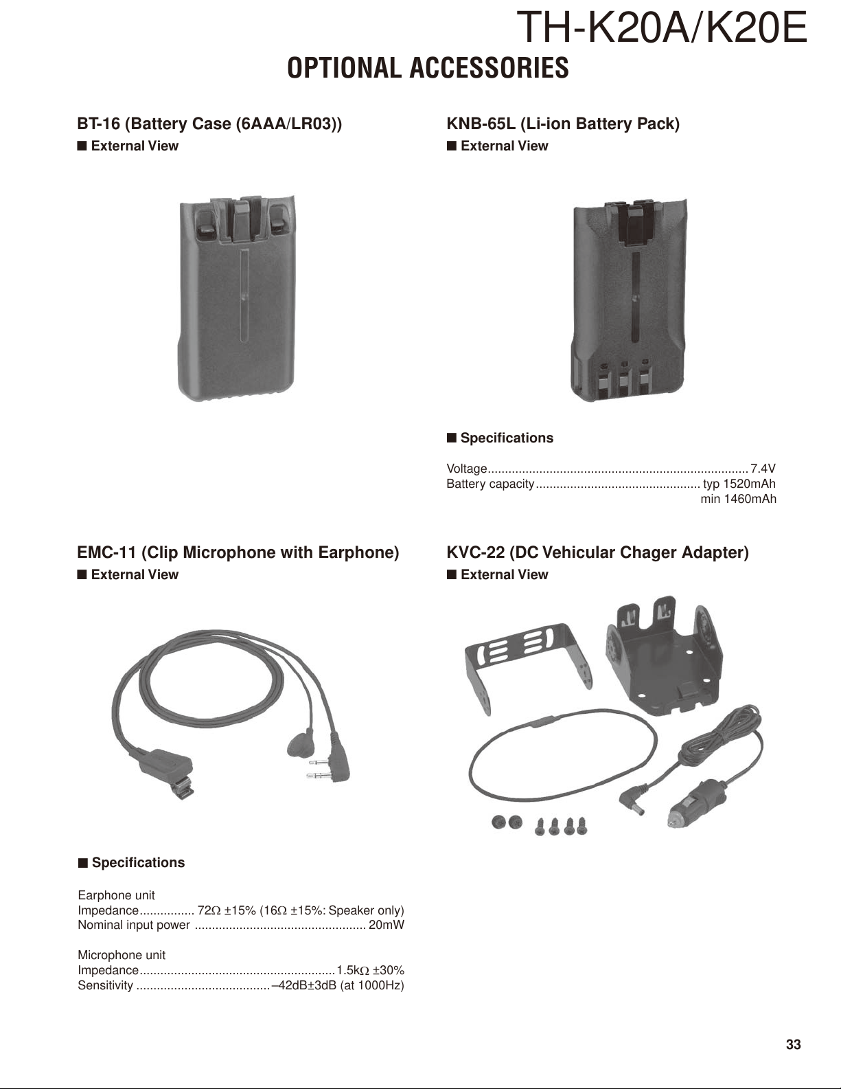
TH-K20A/K20E
OPTIONAL ACCESSORIES
BT-16 (Battery Case (6AAA/LR03))
External View
■
KNB-65L (Li-ion Battery Pack)
External View
■
Specifi cations
■
Voltage ............................................................................ 7.4V
Battery capacity ................................................ typ 1520mAh
min 1460mAh
EMC-11 (Clip Microphone with Earphone) KVC-22 (DC Vehicular Chager Adapter)
External View
■
Specifi cations
■
Earphone unit
Impedance ................ 72 ±15% (16 ±15%: Speaker only)
Nominal input power .................................................. 20mW
External View
■
Microphone unit
Impedance .........................................................1.5k ±30%
Sensitivity .......................................–42dB±3dB (at 1000Hz)
33

TH-K20A/K20E
MEMO
34

TH-K20A/K20E
SPECIFICATIONS
General
Guaranteed range (MHz) TX & RX 144~148 (K/M) / 144~146 (E)
Operation Frequency range (MHz)
Mode F3E, F2D
Antenna impedance 50
Operating temperature range –20°C ~ +60°C (+4°F ~ +140°F)
Operating Voltage DC 6.0 ~ 9.0V (7.4V nominal)
Frequency stability Within ±2.5ppm
Dimensions W x H x D (projections not included) <with KNB-63L> 54 x 111.7 x 25.3 mm / 2.13 x 4.4 x 1.0 in
Weight <with KNB-63L> Approx. 210g / 7.4oz.
Transmitter
RF output power <with KNB-63L/ KNB-65L>
Modulation Reactance
Maximum frequency deviation Within ±5kHz
Spurious emission Less than -60dB
Modulation distortion Less than 5% (300Hz~3kHz)
Microphone impedance 2k
Receiver
Circuit type Double super heterodyne
Intermediate Frequency (IF) 1st IF: 38.85MHz 2nd IF: 450kHz
Sensitivity (12dB SINAD) Less than 0.16µV
Squelch sensitivity Less than 0.13µV
Selectivity
Audio output More than 400mW (8/ 10% distortion)
Note: All specifi cations (General, Transmitter and Receiver) are guaranteed within the amateur radio band.
Guaranteed frequency range .............................................................. 144~148MHz (K,M)
144~146MHz (E)
TX 136~174 (M) / 144~148 (K) / 144~146 (E)
RX 136~174
High 5.5W
Medium 2W
Low 1W
-6dB More than 10kHz
-50dB Less than 28kHz
35

TH-K20A/K20E

JKLMNOPQRSIHGFEDCBA
TH-K20A/K20E PC BOARD PC BOARD TH-K20A/K20E
1
1
TX-RX UNIT (X57-821X-XX) 0-11: K 0-20: M 2-71: E
2
3
4
5
6
7
8
9
Component side view (J79-0325-09)
J79-0325-09
D419
R448
D409
D408
D405
D421
D404
R449
R451
R450
D423
D425
CV
R433
D410
R432
D411
R431
D406
D418
D420
D422
D424
D415
MIC300
C344
D416
76
75
D407
CN202
100
1
5R
Q400
R422
C412
C411
F424
R447
D417
R425
X400
C415
IC401
25
MODE
26
CN304
CN303
GND
RESET
51
50
CP1
5M
D301
C352
F300
+B
+B
IC305
GND
TX-RX UNIT (X57-821X-XX) 0-11: K 0-20: M 2-71: E
Component side view (J79-0325-09)
C423
R440
R443
C383
1
IC308
R377
3
C380
C358
4
IC306
5
C365
C366
C354
4
3
CN300
R362
C329
Q304
5M
S
1
2
C364
C363
2
SPK
SPG
1
Q308
5T
R379
D304
D302
3
1
D
D
G
C377
5
C375
4
SB
R372
G
C322
C321
R323
R358
R351
R365
R364
S
R355
R363
5C
C376
C374
R374
GND
C304
R309
R350 and
C356
R360
Q303
R305
D305
Q305
G
S
C359
C301
D
S
G
D
C367
C369
18
19
IC300
24
1
R300
R301
D300
C351
R354
C353
R370
13
6
R302
C302
R310
C307
12
7
R308
R368
R304
R376
6
10
Q302
C305
R307
C306
IC307
R303
R366
C372
C373
Q301
R359
C334
R339
C342
R347
C379
5
1
Q306
R378
C360
R367
SB
R335
R337
R336
C333
R338
C336
1
IC304
45
R340
C339
R345
R346
R342
C341
C314
R318
C340
R353
C421
R441
C381
D
G
S
D
F301
Q300
R357
C312
R315
C310
R312
C371
C335
R470
R314
C311
5
4
IC301
8
1
R311
R313
C308
R466
R389
C425
C332
C337
C338
R341
R317
C313
8
R316
R446
R380
R445
2
3
4
5
6
7
D427
D426
8
9
10
11
12
13
14
Ref. No. Address
IC300 6O
IC301 8Q
IC304 6P
IC305 6M
IC306 5N
IC307 4P
IC308 4N
IC401 6J
Q300 6Q
Q301 5P
Ref. No. Address
Q302 5P
Q303 4O
Q304 7N
Q305 4O
Q306 5P
Q308 4N
Q400 7H
D300 8O
D301 5M
D302 5N
Ref. No. Address
D304 5N
D305 9O
D404 5C
D405 5D
D406 5E
D407 5F
D408 5D
D409 5E
D410 5E
D411 5E
Ref. No. Address
D414 10J
D415 2J
D416 4G
D417 8G
D418 3F
D419 3D
D420 5F
D421 5D
D422 7F
D423 7D
Ref. No. Address
D424 9F
D425 9D
D426 8R
D427 7R
D414
Component side
Layer 1
Layer 2
Layer 3
Layer 4
10
11
Foil side
12
13
14

JKLMNOPQRSIHGFEDCBA
TH-K20A/K20E PC BOARD PC BOARD
1
TH-K20A/K20E
1
TX-RX UNIT (X57-821X-XX) 0-11: K 0-20: M 2-71: E
2
3
4
5
6
7
8
9
Foil side view (J79-0325-09)
C141
C345
VR300
Q404
Q403
R453
R452
C424
S419
J301
C357
S418
L110
+
C347
PTT
C139
C140
C138
L109
C137
C136
C157
D102
R128
J300
D101
C317
C320
R325
R126
C325
S417
MONI
L214
L213
C261
C427
C428
C129
R243
8
1
R402
D203
C256
R241
R414
IC400
R415
L114
C259
R405
5
4
R240
C419
R238
Q204
G
G
C255
R239
C417
C160
C154
C253
S
D
D401
C420
L108
C135
C134
L107
L112
C144
R319
C318
R388
R320
5
4
IC302
1
8
R386
C319
R385
R322
R326
C324
5
4
IC303
1
8
C328
R328
R387
C326
D103
R321
C327
R327
R329
R330
R361
C316
R369
C361
D105
R119
C146
D104
L115
C133
C265
C406
C407
C404
C405
R438
Q401
C127
R236
R439
C418
R437
Q402
R129
R237
R248
C386
R382
C125
L113
C254
R332
C331
C251
R464
R444
R127
R235
L211
R442
C330
D201
C250
R334
R125
R383
R331
C249
R333
C247
R234
C248
R233
C402
R130
C151
D200
C246
R401
C162
C161
C152
R400
C245
C323
R403
C204
R324
R121
C153
L106
L209
CD200
TH101
C272
R419
R251
C273
C413
D204
C203
R204
C271
C414
R465
C270
Q103
R207
L217
R205
R232
R203
C211
GD
C244
C205
R201
C202
R231
Q200
R115
C115
C150
C207
8
9
TX-RX UNIT (X57-821X-XX) 0-11: K 0-20: M 2-71: E
Foil side view (J79-0325-09)
C105
R116
C240
R230
CF200
C206
R206
C209
C113
R246
R229
R252
R114
IC200
R112
R113
G
Q203
C208
C233
SG
D
C214
R208
C212
L105
F101
D
C112
C213
C239
R253
1
16
S
Q102
C156
R120
R228
C201
R249
R210
C110
R227
C237
R200
R213
L202
G
R111
C109
C159
R124
R247
C200
C221
C108
L104
R109
Q104
C235
L206
R226
C217
TH200
R108
C155
R215
C104
R225
Q202
C215
C107
C
E
C232
R104
C266
L205
C228
R220
C223
C106
Q101
R216
R103
C385
C234
R221
R105
E
B
Q307
XF200
R43
C216
C218
R212
L103
C227
R28
R107
C148
C147
R101
R27
C48
L200L201
R102
C382
C231
C219
C220
C102
L204
C230
C229
R41
C49
C44
C101
C384
+
L101
C226
Q201
L215
C37
C38
R24
C34
D8
R22
R26
L11
C36
R25
X1
C50
R214
R218
R11
C18
C47
C33
D7
Q2
+
C16
D6
C21
L2
D1
D2
L5
L1
C6
D3
C1
L3
16
C39
+
1
L13
C45
C51
R39
R23
R21
C32
Q5
C26
R20
R19
C13
C5
L4
R8
D5
D4
Q1
C8
R6
R5
IC1
C43
C41
C28
C29
C31
C27
L9
R15
R10
D
Q3
G
S
C7
C15
C10
L6
C17
C19
L8
R12
C20
R48
C9
D11
C4
R2
R9
R35
R37
R38
9
R32
R34
C42
8
R30
C46
R40
Q7
R45
R46
2
3
L10
C25
R14
Q4
C23
C12
C22
+
R18
C11
D9
D10
R47
C2
C3
R3
R4
R7
4
5
6
7
R33
R36
R31
Q6
8
9
10
11
12
13
14
Ref. No. Address
IC1 8Q
IC200 8M
IC302 6G
IC303 7F
IC400 8I
Q1 6Q
Q2 4P
Q3 5Q
Q4 4Q
Ref. No. Address
Q5 3Q
Q6 8R
Q7 9Q
Q101 4N
Q102 3N
Q103 4L
Q104 4N
Q200 8M
Q201 9O
Ref. No. Address
Q202 8N
Q203 6M
Q204 6J
Q307 4O
Q401 9J
Q402 8J
Q403 8C
Q404 7C
D1 5P
Ref. No. Address
D2 5P
D3 6P
D4 5Q
D5 5Q
D6 5P
D7 4P
D8 3P
D9 5R
D10 6R
Ref. No. Address
D11 6Q
D101 4F
D102 4F
D103 4G
D104 5H
D105 4G
D200 6K
D201 6K
D203 5I
Ref. No. Address
D204 6L
D401 8J
J79-0325-09
Component side
Layer 1
Layer 2
Layer 3
Layer 4
Foil side
10
11
12
13
14
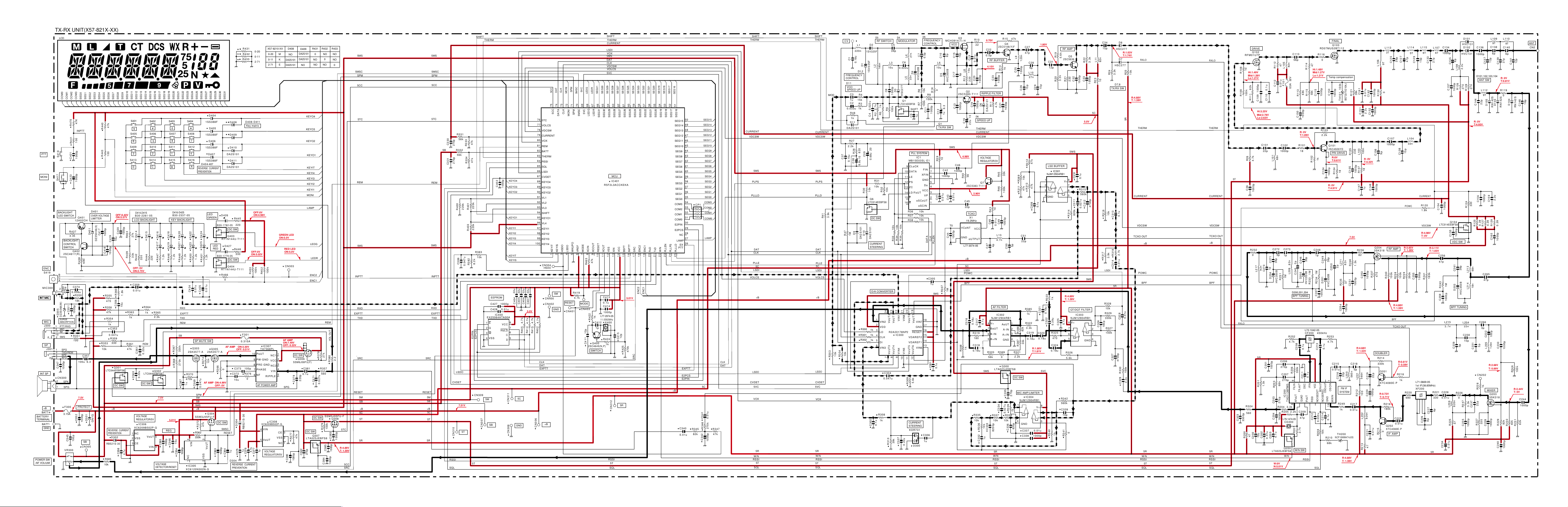
PTT
MONI
ENC
S419
MIC300
INT MICINT MICINT MIC
MIC
J300
INT SP
+B
BATT+
BATTERY
TERMINAL
BATT
GND
POWER SW
/AF VOLIUM
TX-RX UNIT(X57-821X-XX)
LCD
COM0
COM1
COM2
COM3
SEG0
SEG1
SEG2
47K
R470
INPTT
100
R441
S418
1000p
C421
S417
C423
1000p
BACKLIGHT
LED SWITCH
R437
3.3k
BACKLIGHT
CONTROL
SWITCH
2SC4617(R)
B
C
A
2
0.056u
C344
270p
1
C351
D305
DZ2S068(M)
SURGE
ABSORPTION
PTT/RXD
1
MIC
3
11
IM
10
5MS
2
SP
J301
1
SPG
3
TXD/REM
SPK
4
2
AFO
C347
1000p
CN300
2
+
SPK
1
-
SPG
F300
3.15A
-
C345
VR300
Q401
12A02CH
Q402
C374
R350
18k
1000p
R351
100
PROTECT
C352
100p
100u
7.5V
R438
C357
1000p
CN305
SB
D401
OVER VOLTAGE
LIMITTER
D401
680
6.3
D301
SEG3
SEG4
C417
DZ2S036(0)
R353
10k
GN1G
SEG5
SEG6
SEG7
SEG8
47k
R440
100
R443
OFF:0.40V
ON:5.57V
C420
1000p
10u
C419
C418
1000p
R360
R355
470
C356
R358
47k
R354
1k
C353
0.047u
R359
330
Q301
LTC044EEBFS8
DC SW
+B
REVERSE CURRENT
PREVENTION
D302
RB521S-30
R305
10k
C358
SEG9
1000p
1.8k
10u
SEG10
R464
R439
R363
1k
R361
47k
4.7u
SEG11
SEG12
SEG13
S401
9
S405
6
S409
3
S413
D
D414,D415
B30-2261-05
LCD BACKLIGHT
27k
D414
33k
330
R442
OFF: 0V
ON:2.75V
C359
0.01u
REM
C361
C360
0.22u
DC SW
VOLTAGE
REGULATOR/5V
IC306
XC6209B502P-G
1NC
2VSS
3CE
SEG14
SEG15
SEG16
SEG17
SEG18
SEG19
SEG20
S402 S403 S404
#
S406
S410
0
S407
8
5
S411
1
S414
D415
S415
C
D416
B
D416-D425
B30-2337-05
KEY BACKLIGHT
D418D419
D417
1.2k
1.2k
R447
220
R444
R448
R364
R365
1k
2.2k
0.22u
R367
R368
Q302
LTC044EEBFS8
7.5V
5.01V
REG
5
VoUT
10u
C365
C366
1000p
4VIN
VOLTAGE
DETECTOR/RESET
SEG21
SEG22
D420
D421
1.2k
R449
RXD
EXPTT
TXD
REM
SB
330k
270k
R370
470k
1u
C367
C354
1000p
XC6120N302N-G
SEG23
SEG24
SEG25
S408
7
S412
42
S416
A
REVERSE CURRENT
PREVENTION
D423 D422
1.2k
R450
C424
0.01u
SP MUTE SW
Q303
2SK3577-A
C369
SPM
5M
SB
5MS
+B
SSM3J05FU-F
R362
330k
4
VIN
1NC
IC305
D404-407
D424
D425
C425
0.047u
R372
SEG26
SEG27
1SS388F
1SS388F
1SS388F
1SS388F
LED
GREEN
1.2k
R451
0.01u
2SK3577-A
R374
AF AMP
Q304
47k
3
VoUT
2VSS
SEG28
D404
D405
D406
D407
Q305
10k
SEG29
SEG30
D426
B30-1782-05
RT1N144U-T111
LED
RED
B30-1779-05
RT1N144U-T111
R466
R366
ON:4.99V
OFF: 0V
DC SW
5MSC
C363
1000p
SEG31
D408
D409
D410
DA2S101
D411
DA2S101
R445
220
DC SW
Q403
D427
R446
330
DC SW
Q404
0
AF AMP
OFF: 0.51V
C373
0
C372
10u
RESET
1u
C364
D304
REVERSE CURRENT
PREVENTION
R431
R432
R433
F301
0.315A
ON:3.30V
D304
C375
D408-D411
Key matrix
OFF:0V
ON:5.02V
R453
10 PoUT
100p
R376
0
RB521S-30
1u
4.7u
C376
0-20
0-11
2-71
OFF:0V
ON:4.98V
100k
R452
IC307
TA7368PL
9 PW-GND
8 PRE-GND
7PHASE
6NF
AF POWER AMP
XC6209B502P-G
4 VIN
5 VoUT
VOLTAGE
1u
C377
REGULATOR/5V
X57-8210-XX
0-20
0-11
2-71
100k
NC1
VCC
NC2
VIN
RIPPLE
IC308
M
K
DA2S101
E
DA2S101
GREEN LED
ON:5.0V
RED LED
ON:5.0V
CN303
AF AMP
ON:7.49V
OFF: 0.33V
1
2
3
4
5
SPG
3CE
2VSS
1NC
D408
NO
DC SW
Q306
SSM6J08FU(F)
C379
47k
R377
C380
1000p
D409
DA2S101
DA2S101
NO
KEYO4
KEYO3
KEYO2
KEYO1
KEYIT
KEYI4
KEYI3
KEYI2
KEYI1
MONI
LAMP
C381
0.1u
220p
DC SW
LTA023JEBFS8
270p
C382
R431
LEDG
LEDR
ENC2
ENC1
Q307
0
NO
NO
C371
DC SW
R432
NO
0
NO
REM
27k
R378
R357
560
0.027u
SSM3J05FU-F
100k
R379
C385
C384
R433
NO
NO
0
VOL OUT
2.2
R380
Q308
C383
1000p
1000p
1000p
R:4.89V
T: 1.59V
SHIFT
THERM
5MS
5MSC
SPM
5CC
5TC
REM
5MS
INPTT
RXD
EXPTT
TXD
5RC
5RC
5MS
5MSC
SPM
5CC
5TC
REM
5MS
INPTT
RXD
EXPTT
TXD
5VC
SPM
DAT
5CC
CLK
MONI
5MSC
71
72
73
74
75
5CC
76
77
R331
56k
270p
R332
270p
47k
R333
56k
47k
R334
C330
SB
C331
78
79
80
81
82
83
84
85
86
87
88
89
90
C402
1000p
KEYO4
KEYO3
KEYO2
91
92
R400
220k
R401
220k
KEYO1
93
94
95
96
LSDO
C386
R403
0.047u
R382
220k
R383
8.2k
E2PIN
10k
E2PCS
EEPROM
C427
1000p
0.01u
C428
IC400
EX25064ATA00A
1S
VCC
2Q
HoLD
3W
4VSS
KEYI1
KEYI2
KEYI3
KEYI4
KEYIT
KEYIS
22u
C404
8
7
6
C
5
D
22u
C405
22u
C406
4.7k
R405
5.0V
R414
22u
C407
4.7k
4.7k
R415
97
98
99
100
4.7k
R402
CLK
DAT
EXPTT
DATA
5TC
VOLCS
VDCSW
CURRENT
VOX
REM
BATT
THERM
RSSI
SQL
LSDI
CVDET
KEYO4
KEYO3
KEYO2
VL1
VL2
VL3
SHIFT
KEYO1
VL4
KEYI1
KEYI2
KEYI3
KEYI4
KEYIT
KEYIS
HSDO
123456789
CN304
HSDO
5M
CN400
CN402
GND
CLK
RESET
CN401
MONI
LSDO
SPM
WKUPO
R419
4.7k
70
5MSC
VREF
MODE
69
5VC
MODE
R465
CN403
12p
C411
CVDET CVDET
RESET
5M
SB
+B
5C
5T
5TC
5R
RESET
7.51V
CN309
5M
SB
CN307
5T
CN311
CN308
GND
5C
+B
CN306
5M
SB
+B
5C
5T
CN310
5R
SHIFT
THERM
CURRENT
LSDI
VOX
5MS
DAT
CLK
VDCSW
VOLCS
5VC
SEG30
SEG29
SEG28
SEG27
SEG26
SEG25
SEG24
SEG23
SEG26
60
SEG25
INPTT
59
SEG24
5RC
58
SEG23
ENC2
SEG22
57
SEG22
ENC1
SEG31
LEDG
LEDR
61
62
63
64
65
66
67
68
LEDR
LEDG
SEG31
XCIN
XCOUT
RESET
101112131415161718192021222324
SEG27
SEG28
SEG29
SEG30
MCU
IC401
R5F2L3ACCKEKA
XOUT
VSS
XIN
VCC
BSFT
47k
ENC2
5.01V
ENC1
R422
L77-2974-05
1k
11.0592MHz
C412
C413
0.1u
C414
1000p
X400
1p
12p
C415
R424
Q400
1k
2SC4649(N,P)
SWITCH
R425
470k
5RC
5R
CN312
SEG21
56
SEG21
RxD
SEG20
55
SEG20
TxD
SEG19
54
SEG19
W/N
SEG18
53
SEG18
PLLEN
SEG17
52
SEG17
PLLPS
+B
SEG16
51
SEG16
SEG15
SEG14
SEG13
SEG12
SEG11
SEG10
SEG9
SEG8
SEG7
SEG6
SEG5
SEG4
SEG3
SEG2
SEG1
SEG0
COM3
COM2
COM1
COM0
E2PIN
E2PCS
LAMP
PTT
PLLLD
25
NC
EX
EXPTT
E2PCS
E2PIN
C340
0.01u
SEG15
50
SEG14
49
SEG13
48
SEG12
47
SEG11
46
SEG10
45
44
43
42
41
40
39
38
37
36
35
34
33
32
31
30
CP1
SEG9
SEG8
SEG7
SEG6
SEG5
SEG4
SEG3
SEG2
SEG1
SEG0
COM3
COM2
COM1
COM0
29
28
27
LAMP
26
CLK
DAT
5C
C341
0.01u
R346
270k
R345
82k
C342
1000p
R347
47k
SHIFT
THERM
CURRENT
VDCSW
5MS
PLPS
PLLLD
DAT
CLK
PLLE
LSDI
VOLCS
LSDO
5VC
VOX
5C
+B
5R
W/N
RSSI
SQL
5T
5CC
5RC
RSSI
SQL SQL
5T
RSSI
5T
SHIFT
THERM
VDCSW
5MS
PLPS
PLLD
DAT
CLK
PLLE
5C
LSDI
VOLCS
+B
LSDO
CVDET
5VC
VOX
5R
W/N
RSSI
5T
SQL
R41
MOD
3.9k
R303
10k
CV
FREQUENCY
CONTROL
D11
C37
R47
10k
R304
220n
C1
VCO
SPEED UP
C3
1u
C2
0.033u
R48
1k
D11
DA2S101
R27
2.2k
R28
0.15u
C38
D9
1M
L1
0.18u
D1,2
R4
15k
R3
1k
820
10
6.8u
R300
R301
R302
D2
1SV325F
D1
1SV325F
C4 0.022u
C39
10k
R30
Q6
LTC014EEBFS8
D10
DA2S101
CURRENT
STEERING
1k
1k
1k
D3
RF SWITCH
L2
10u
180n
C8
R6
R5 1k
R2 2.7k
0.68u 20
R31
10k
R32
10k
DC SW
DA2S101
D/A CONVERTER
24
1
VIN2
2
VDD
3
LD
4
CLK
5
DI
6
VIN3
7
C304
0.047u
R308
1k
0.1u
C302
D4
MODULATOR
C5
39p
L4
27n
C6
L3
0.022u
D4
L5
22n
D3
1000p
HSC277
Q1
LTC014EEBFS8
SHIFT
100k
C9
PLL SYSTEM
MB15E03SL-E1
9 CLoCK
10 DATA
11 LE
12 PS
13 ZC
14 LD/FoUT
15 P
16 R
R36
R37
R38
10k
10k
10k
R34
R35
R33
19
20
21
23
VIN822VIN1
VIN7
VoUT7
VoUT8
VoUT1
VoUT2
R2A20178NP2
IC300
GND
RESET
VDAREF2
VDAREF1
VoUT38VoUT49VIN410VIN511VoUT512VoUT6
5.6k
R309
CURRENT
STEERING
KDR731
39k
C307
R310
0.22u
D300
D5
C7
HVC350B
R8
R7
1u
IC1
XFIN
GND
VCC
oSCoUT
oSCIN
10k
10k
10k
VIN6
FREQUENCY
CONTROL
0.5p
R18
10k
R9
100k
100k
C11
1000p
8
FIN
7
6
5
Do
4
3
VP
2
1
CLK
DATA
C305
1u
5MS
18
17
16
15
14
13
C301
C306
1u
L6
10u
0
Q1
TX/RX SW
R39
C41
PLLEN
0.1u
MCH3914(7)-H
C10
D5
6.3
C12
1u
10
C42
1000p
0.01u
R307
VCO
8p
C15
C17
HVC350B
C13
5MS
C46
1000p
C43
0.01u
T0
C44
1000p
1M
Q3
10p
C19
L8
10u
9p
R12
220
Q2
2SC5383-T111
C18
1000p
C16
22u 10
4.98V
56
R40
2SC5383-T111
C45
22p
TCXO
X1
19.2MHz
VCoNT
GND
oUTPUT
L77-3074-05
+B
5C
LSDI
POWC
BPF
C316
R319
C318
1k
R388
0.18u
0.70V
C22
0.5p
RF BUFFER
4.15V
R11
DA2S101
R15 47k
2SC5108(Y)F
R14
C23
1000p
4.7k
C21
Q4
1k
1000p
C25
R22
C33
3.3k
1000p
R23
C34
15p
82n
L11
10
1.80V
C27
47p
L9
120n
C28
9p
L10
1000p
27n
15p
15p
C29
C26
C31
RF AMP
Q5
R19
5.6k
2SC5636
12p
3.3k
C32
R20
R21
330
1000p
5C
5.0V
R10
22
0.01u
C20
1000p
D6
SPEED UP
THERM
CURRENTCURRENT
VDCSW
1000p
RIPPLE FILTER
D6
5MS
VOLTAGE
REGULATOR/3V
Q7
2.90V
VCC
C47
C48
R43
4p
10
0.01u
L13
4.7n
R45
R46
C49
33k
100k
1000p
C50
5p
R389
R311
C51
22p
47k
R312
15k
R313
47k
47k
C308
0.1u
LSD BUFFER
IC301
NJM12904RB1
1
2
-
3
4
GND
C310
0.1u
8
V+
7
R315
6
++-
5
R314
C311
820k
560k
0.027u
C312
4700p
5MS
R:4.89V
1k
T: 1.59V
R323
0.18u
180
C317
0.1u
5MS
8V+
7BoUT
6B-IN
5B+IN
R320
56k
AF FILTER
IC302
NJM12904RB1
AoUT
A-IN
A+IN
GND
R369
0
Q300
LTA023JEBFS8
R385
C321
R:1.80V
T:1.81V
C320
0.18u
0.18u
C322
R325
C324
0.18u
1k
R322
1
3.3k
2
82k
R386
C319
3
0.18u
4
33k
R387
R321
2.2k
0.39u
470
C325
QT/DQT FILTER
NJM12904RB1
8V+
0.1u
7
6
5
R326
5.6k
IC303
-++
-
GND
1
C326
2
3
4
5VC
DC SW
MIC AMP/LIMITER
C335
270p
IC304
NJM12904RB1
1
C334
R339
1k
R335
10k
R336
C332
10k
1u
0.027u
R338
R337
10k
10k
C333
8200p
5R
W/N
RSSI RSSI
C336
820p
4
GND
-
C337
C338
8
V+
+
+
-
5
0.01u
1000p
R340
R342
560k
C339
10p
0
1k
R341
SQL SQL
R316
R317
LSDI
R328
10k
R329
330k
180p
R327
100k
HSC277
R24
D7,8
TX/RX SW
10k
C313
R318
3.9k
C314
5R
C327
D8
HSC277
D7
3.3k
0.1u
2.7k
0.01u
C328
4700p
R:1.03V
T:1.74V
RXLO
10k
R25
R:4.88V
T: 1.59V
5R
THERM THERM
VDCSW
TCXO OUT
+B
POWC
0.01u
100k
R330
2.2u
C329
5R
W/N
5T5T
RXLO
CURRENTCURRENT
VDCSW
TCXO OUT
+B
POWC
BPFBPF
5R
W/N
RSSI
5T
SQL
L110
C136
1000p
D101,102,103,104
ANT SW
270
L112
9T
22p
C144
R: 0V
T:4.93V
C156
330
0.39
R127
R125
68n18n
C265
47p
C266
3p
5p
C231
CN202
1k
R228
22p
C237
330
R227
C137
D105
1000p
C232
L205
MIXER
C239
L109
9T
C138
6p
12p
RN142S
C159
0.39
R129
C160
100p
120n
R:2.68V
T: 0.89V
Q203
3SK318
1000p
D103
2.2u
C139
R: 0V
T:0.81V
R119
0.39
1000p
C233
R229
C240
9T
C140
6p
27p
0
RN142S
1000p
82k
1000p
R230
C141
D104
R246
R:2.44V
T: 0V
82k
12p
C146
RN142S
100k
C244
1000p
82k
R231
ANT
CN2
18p
1000p
L215
2.7n
1M
1000p
6p
C135
L108
C157
1000p
Q104
C155
1000p
VDC SW
C261
D203
BPF TUNING
C229
R226
820n
L206
47
R225
0.01u
D101
HVC131
D102
HVC131
2.2u
R126
39p
HVC350B
L204
C230
5p
0
270
22n
10p
R247
C235
R128
R124
L213
L214
3.3k
1000p
FINAL
Q103
68k
1000p
R114
R115
47
Hi:1.48V
Mid:1.27V
Lo:1.21V
56k
R102
RD07MUS2BT112
R116
0
Temp compensation
C153
C115
1000p
R103
2.2k
Q101
2SC4926YD
PRI DRIVE
R:0V
1k
T:0.61V
C104
1000p
R: 0V
T:4.91V
1000p
R104
100k
-t
B57331V2104J
TH101
18
R121
R105
C105
39k
330
1000p
C161
C151
L103
R107
C147
100n
R: 0V
T:4.32V
18
1u
DRIVE
Q102
RFM01U7P
10
Hi:1.49V
R108
Mid:1.28V
Lo:1.21V
0.1u
1000p
100k
R109
R111 82k
C110
C109
Hi:3.25V
Mid:2.78V
Lo:2.63V
C101
22p
R26
4.7k
5T
C36
1000p
L101
R112
C112
68n
47
0.01u
C102
1000p
L105
F101
C113
56p
82n
0.5A 32V
R113
C150
R: 0V
T:1.09V
R101
18
0.01u
2.2u
C162
C152
C148
1000p
1000p
C106
1000p
L106
R130
L113
3T
9T
0
C107
1000p
9p
7.5V
R236
82
1.5k
1000p
R:4.68V
T: 1.53V
L201
R212
C253
560n
100
L202
R213
1000p
C219
C220
820n
C221
47
Q204
3SK318
470
R237
DOUBLER
R214
330k
22p
1000p
0.01u
R240
Q201
KTC4080E-P
R:0.72V
T: 0.71V
R216
180k
Q202
KTC4080E-P
0
R215
IF AMP
RXLO
C323
R324
560
3300p
R200
R232
0
47
C200
L217
5R
82n
R201
10u
C202
C270
C201
1.5k
0.01u
C273
C272
3p
1p
C271
39p
1p
D204
R251
HVC350B
C206
270p
1000p
C207
270p
68k
R203
270p
C203
R204
R205 2.2k
C204
L79-1474-05
1800p
CD200
0.1u
C205
Q200
LTA023JEBFS8
W/N
W:0V
N:5.01V
1M
R252
IC200
TA31136FMG
3.3k
4.7k
2p
82n
L209
C245
D200,201,204
BPF TUNING
C208
330k
R206
8
FILIN
AFoUT
9
C209
R207
W/N SW
C246
D200
0.1u
C211
FILoUT
QUAD
47p
2.7k
RSSI
C248
39p
1M
HVC350B
R233
L72-1042-05
CF200
0.1u
IFIN
DEC
RSSI
IFoUT
C212
1p
1M
R234
C247
450kHz
C213
VCC
NOISEDET
0.033u
R208
SQL
C249
D201
1000p
R253
4.7k
0.1u
MIXoUT
OSCoUT
GND
NOISEREC
C214
18k
R210
68k
39p
L211
2p
C250
R235
HVC350B
C254
C215
0.01u
C216
1
FM IF
OSCIN
SYSTEM
MIXIN
R249
16
1k
0.1u
TH200
NCP18WM474J0S
-t
R:4.88V
T: 1.59V
22p
82n
47
1000p
L200
R248
C251
C218
5p
560n
C217
0.01u
C125
RF AMP
100k
R:4.88V
T: 1.59V
BPF
TCXO OUT
R238
C223
0.01u
39p
R:0.61V
T: 0.59V
R218
1k
C127
C108
100k
L114
47p
L104
33n
15p
POWC
R:3.85V
T: 1.26V
R239
R220
680
5T
C129
CURRENT
390k
C255
L71-0669-05
1st IF(38.85MHz)
XF200
L115
6T
15p
R120
1.8k
VDCSW
R:4.98V
T: 0V
1000p
C226
R241
C133
R:3.11V
T: 1.03V
180k
R221
C227
8p
5R
L107
330
C134
6T
1000p
27p
C154
LTC014EEBFS8
C256
47p
R243
C259
C228
0.01u
6p
C234

TX-RX UNIT (X57-821x-xx )
D426
B30-1782-05
BUSY
(GRN)
D427
B30-1779-05
TX
(RED)
B38-0939-05
LCD
D414,D415 B30-2261-05
D416~D425 B30-2337-05
LCD/KEY BACKLIGHT
KEY MATRIX
PTT
MONI
S419
W02-3766-05
ENC
BATT+
7.5V
BATT-
VR300
R31-0684-05
VOL/PSW
S418
S417
F300
3.15A
SB
5MS
DCSW
Q403
LTC014EEBFS8
LEDG
5MS
DCSW
Q404
LTC014EEBFS8
LEDR
COM0~COM3,SEG0~SEG31
Q401
12A02CH
2SC4617(R)
DCSW DCSW
SB
D404~D407
1SS388
D408~D411
MA2S111-F
DIODE
MATRIX
INPTT
MON
ENC1
ENC2
+B
PROTECT
D301
GN1G
D302
RB521S-30
PROTECT
VOLIN
VOLOUT
Q6
LTC014EEBFS8
PLLD
INVERT
2SC5383-T111
Q402
LAMP
LEDG
LEDR
PLLE
DAT
CLK
KEYI1~KEYI4,KEYIS,KEYIT
KEYO1~KEYO4
BATT
RESET
EXPTT
INPTT
BATT
5M
IC306
XC6209B502P-G
AVR
5V
RESET
IC305
XC6120N302N-G
Q7
SB
MB15A02PFV2E1
PLPS
PLLE
DAT
CLK
LD
3.3V
REG
5C
L77-1944-05
LSDO
IC300(6/8)
R2A20178NP
FREQ
5MSC
5TC
5RC
5CC
PLLD
ENC1
ENC2
MON
D304
RB521S-30
PROTECT
Q304
SSM3J05FU-F
DC SW
5MSC
RESET
IC1
PLL SYSTEM
TCXO
19.2MHz
X1
5C
D/A
CONV.
5MS
XOUT
X400
L78-2974-05
11.0592MHz
5MS
LOOP
FILTER
ASSIST
MCU
IC401
R5F2L3ACCKEKA
XIN
BSFT
SW
Q400
2SC4919-S
IC308
XC6209B502P-G
AVR
5V
5CC
LPF
D4
HVC350B
MOD
5MS
D/A
CONV.
D5
IC300(5/8)
R2A20178NP
HVC350B
VCO oscillation frequency
RX: 174.850~212.845MHz(K,M,E)
TX: 136.000~173.995MHz (M)
144.000~147.995MHz (K)
144.000~145.995MHz (E)
5M
CLK
DATA
E2PIN
E2PCS
EEPROM
IC400
BR255640FV1-W
Q308
DC SW
5TC
Q307
LTA023JEBFS8
DC SW
5RC
Q3
MCH3914(7)-H
D1,D2
1SV325F
VCO
SHIFT
SW
SHIFT
THREM
CURRENT
RSSI
SQL
VOX
LSDI
VDCSW
WIID/NAR
HSDO
SPM
5M
5C
SSM3J05FU-F
5T
5R
Q1
LTC014EEBFS8
D3
HSC277
Q4
2SC5108(Y)F
BUFF
AMP
RIPPLE
FILTER
5C
19.2MHz
WID/NAR
LSDI
VOLIN
2SC5636
Q2
2SC5383-T111
D6
DA2S101
Q201
KTC4080E-P
DOUBLER
5R
SQL
RSSI
L79-1474-05
LTA023JEBFS8
QT/DQT
FILTER
FILTER
CONV.
IC300(2/8)
R2A20178NP
Q5
RF
AMP
5C
DC SW
Q200
AF
D/A
2nd Local
AFO
CD200
D7,D8
HSC277
5T
38.4MHz
IF SYSTEM
CD
IC303
NJM12904RB1
5MS
IC302
NJM12904RB1
5MS
2SC4926YD
TX/RX
SW
5R
VDCSW
1st Local frequency
174.850~212.845MHz(K,M,E)
IC200
TA31136FMG
5R
CF200
L72-1042-05
450kHz
IC300(3/8)
R2A20178NP
MOD
VOX
Q101
PRE
DRIVE
5T
VDC SW
Q104
LTC014EEBFS8
Q202
KTC4080E-P
IF
AMP
5R
VOLOUT
SB
0.315A
D/A
CONV.
VOX DET
D300
KDR731
HSDO
F301
Q102
RFM01U7P
DRIVE
AMP
MCF
38.85MHz
XF200
L71-0669-05
IC307
TA7368FG
AF POWER AMP
DC SW
IC304
NJM12904RB1
MIC AMP
LIMITER
DC SW
5MS
RD07MUS2BT112
F101
0.5A
IC300(8/8)
R2A20178NP
POWC
CONV.
5MS
Q203
3SK318
MIXER
5R
Q306
SSM6J08FU(F)
HSDO
5VC
Q300
LTA023JEBFS8
Q103
FINAL
AMP
CURRENT
D/A
BPF
RF BPF
TUNE
D200,D201,D204
HVC350B
BPF
2SK3577-A
Q301
LTC044EEBFS8
DC SW
SPM
IC301
NJM12904RB1
V REF/
MIC AMP
5C
RX: 136.000~173.995MHz (K,M,E)
TX: 136.000~173.995MHz (M)
144.000~147.995MHz (K)
144.000~145.995MHz (E)
D103-D105
RN1425
D101,D102
HVC131
ANT SW
+B
Q204
3SK318
RF
AMP
5R
IC300(7/8)
D/A
R2A20178NP
CONV.
5MS
Q305
MUTE
SW
Q303
2SK3577-A
MUTE
MUTE
SW
SW
DC SW
IC300(1/8)
R2A20178NP
D/A
CONV.
5T
THREM
BPF
D203
RF BPF
HVC350B
TUNE
Q302
LTC044EEBFS8
-t
TH101
EXPTT
5MS
ANT
J301
E11-0717-05
CN300
J300
E11-0484-05
MIC300
T91-0673-05
MIC
SPG
TXD
SPK
AFO
PTT/RXD
MIC
IM
5MS
EXT
SP
INT
SP
EXT
MIC
INT
MIC
 Loading...